

ST TDA7448 User Manual
TDA7448
Fi
6 CHANNEL VOLUME CONTROLLER
1 FEATURES
■ 6 CHANNEL INPUTS
■ 6 CHANNEL OUTPUTS
■ VOLUME ATTENUATION RANGE OF
0 TO -79dB
■ VOLUME CONTROL IN 1.0dB STEPS
■ 6 CHANNEL INDEPENDENT CONTROL
■ ALL FUNCTION ARE PROGRAMMABLE VIA
SERIAL BUS
2 DESCRIPTION
The TDA7448 is a 6 channel volume controller for
quality audio applications in Multi-Channels Audio
Systems
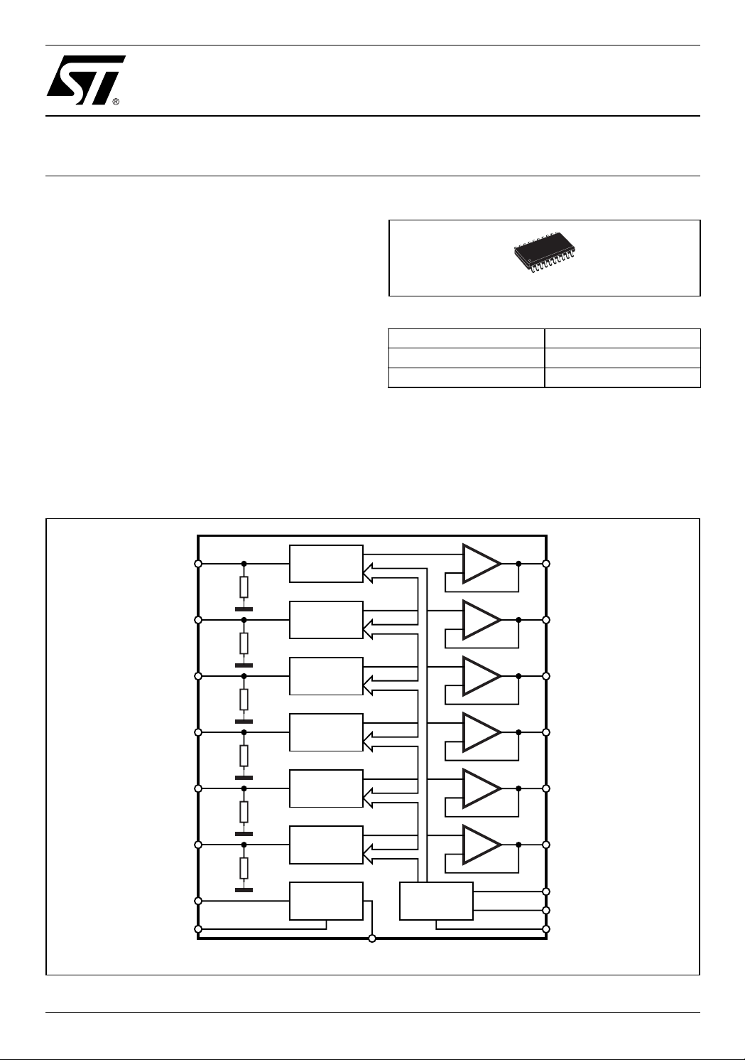
Figure 2. Block Diagram
2
IN1 OUT1
50K
19
IN2
50K
3
IN3
50K
18
IN4
50K
4
IN5
50K
17
IN6
50K
11
GND
CREF
20
VOLUME
VOLUME
VOLUME
VOLUME
VOLUME
VOLUME
SUPPLY
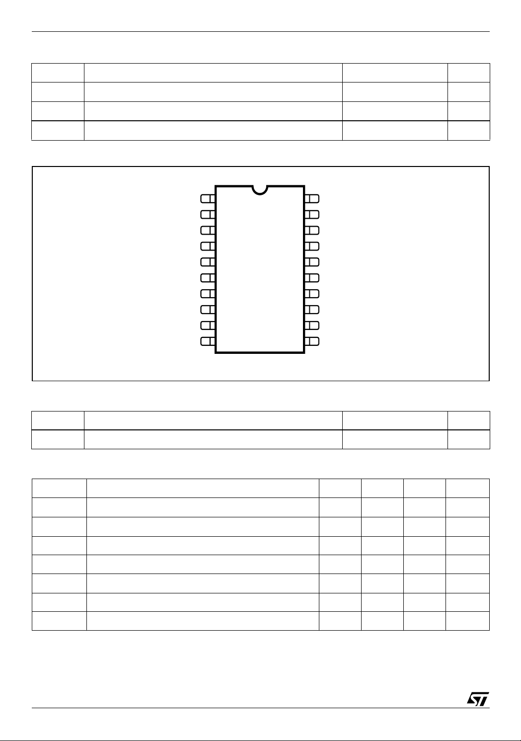
gure 1. Package
SO-20
Table 1. Order Codes
Part Number Package
TDA7448 SO-20
TDA744813TR Tape & Reel
Thanks to the used BIPOLAR/CMOS Technology,
Low Distortion, Low Noise and DC stepping are obtained.
7
14
OUT2
6
OUT3
15
OUT4
5
OUT5
16
OUT6
2
I
C BUS
DECODER
1
V
S
10
9
12
D02AU1396
SCL
SDA
ADDR
June 2004
REV. 3
1/14
TDA7448
Table 2. Absolute Maximum Ratings
Symbol Parameter Value Unit
Operating Supply Voltage 10.5 V
S
Operating Ambient Temperature 0 to 70 °C
Storage Temperature Range -55 to 150 °C
T
V
amb
T
stg
Figure 3. Pin Connection (Top view)
V
S
IN1
IN3
IN5
OUT5
OUT3
OUT1
N.C.
SDA
SCL 10 GND
1
2
3
4
5
6
7
8
9 ADDR
20
19
18
17
16
15
14
13
12
CREF
IN2
IN4
IN6
OUT6
OUT4
OUT2
N.C.
11
D02AU1397
Table 3. Thermal Data
Symbol Parameter Value Unit
R
th j-pin
thermal Resistance junction-pins 150 °C/W
Table 4. Quick Reference Data
Symbol Parameter Min. Typ. Max. Unit
V
S
V
CL
THD Total Harmonic Distortion V = 1Vrms f =1KHz 0.01 0.1 %
S/N Signal to Noise Ratio Vout = 1Vrms 100 dB
S
C
Supply Voltage 4.75 9 10 V
Max Input Signal Handling 2 Vrms
Channel Separation f = 1KHz 90 dB
Volume Control (1dB step) -79 0 dB
Mute Attenuation 90 dB
2/14
TDA7448
Table 5. Electrical Characteristcs
(refer to the test circuit T
Symbol Parameter Test Condition Min. Typ. Max. Unit
SUPPLY
V
SVR Ripple Rejection 80 dB
Supply Voltage 4.75 9 10 V
S
I
Supply Current 7 mA
S
INPUT STAGE
R
V
S
Input Resistance 35 50 65 KΩ
IN
Clipping Level THD = 0.3% 2 2.5 Vrms
CL
Input Separation The selected input is grounded
IN
VOLUME CONTROL
C
RANGE
A
VMAX
A
STEP
E
E
V
A
mute
Control Range 79 dB
Max. Attenuation 79 dB
Step Resolution 0.5 1 1.5 dB
Attenuation Set Error AV = 0 to -24dB -1 0 1 dB
A
Tracking Error AV = 0 to -24dB -1 0 1 dB
T
DC Step adyacent attenuation steps -3 0 3 mV
DC
Mute Attenuation 90 db
AUDIO OUTPUTS
V
V
CLIP
R
Clipping Level THD = 0.3% 2 2.5 Vrms
Output Load Resistance 2 KΩ
L
DC Voltage Level 4.5 V
DC
GENERAL
E
S/N Signal to Noise Ratio All gains = 0dB; V
S
THD Distortion A
Output Noise BW = 20Hz to 20KHz
NO
Channel Separation left/Right 80 90 dB
C
BUS INPUT
V
V
I
V
Input Low Voltage 1V
Il
Input High Voltage 2.5 V
IH
Input Current VIN = 0.4V -5 5 µA
IN
Output Voltage SDA
O
Achnowledge
= 25°C, VS = 9V, RL = 10KΩ, RG = 600Ω, unless otherwise specified)
amb
90 dB
through a 2.2µ capacitor
A
= -24 to -79dB -2.0 0 2.0 dB
V
A
= -24 to -79dB -2 0 2 dB
V
10 15 µV
All gains = 0dB, Flat
= 1Vrms 100 dB
O
= 0; VI = 1Vrms 0.01 0.1 %
V
IO = 1.6mA 0.4 0.8 V
3/14
TDA7448
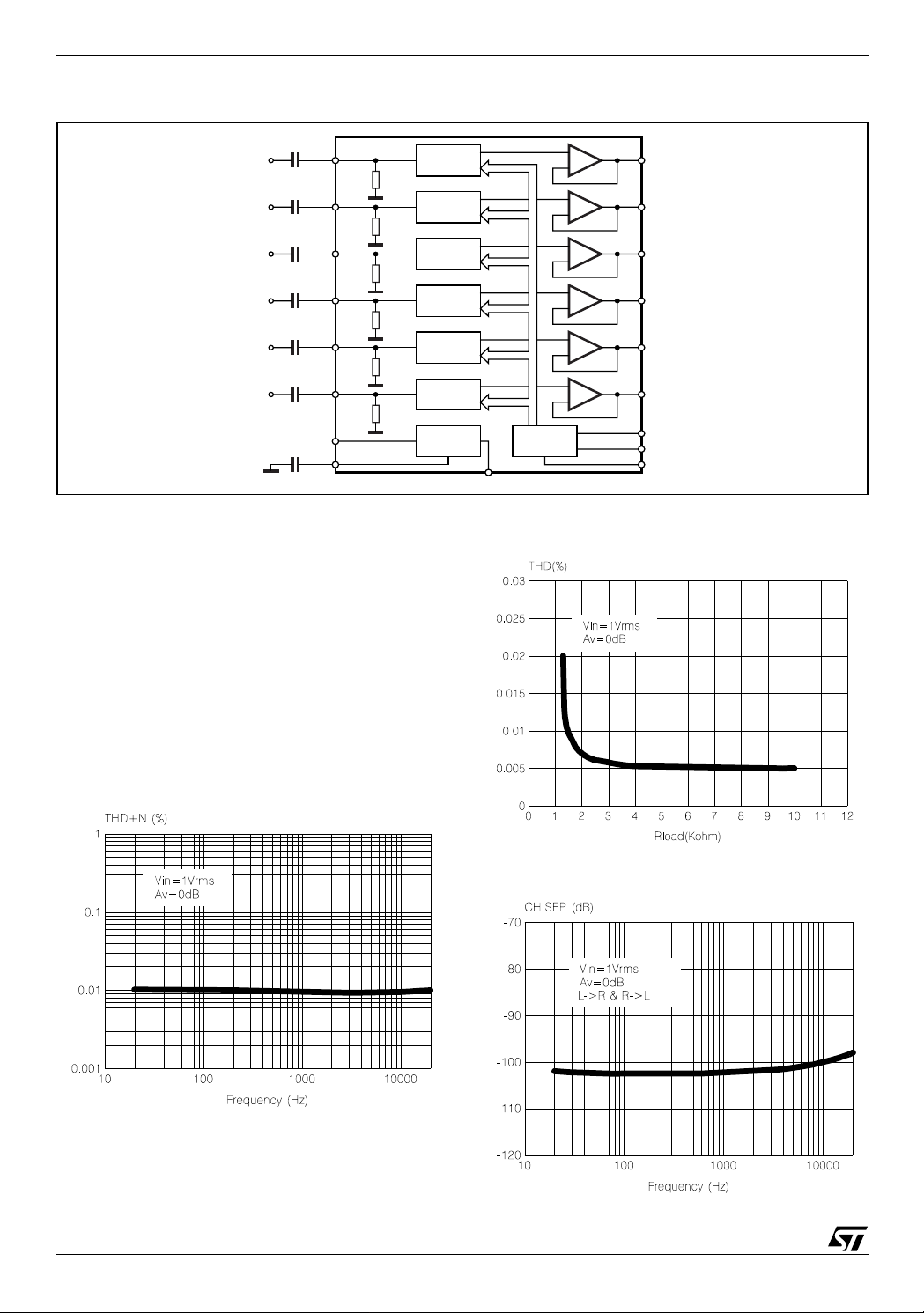
Figure 4. Test circuit
0.47µF
IN1
GND
CREF
2
IN2
19
IN3
3
IN4
18
IN5
4
IN6
17
11
20
50K
50K
50K
50K
50K
50K
VOLUME
VOLUME
VOLUME
VOLUME
VOLUME
VOLUME
SUPPLY
2
I
C BUS
DECODER
1
V
S
IN1
0.47µF
IN2
0.47µF
IN3
0.47µF
IN4
0.47µF
IN5
0.47µF
IN6
10µF
7
14
6
15
5
16
10
9
11
D02AU1406
OUT1
OUT2
OUT3
OUT4
OUT5
OUT6
SCL
SDA
ADDR
3 APPLICATION SUGGESTIONS
The volume control range is 0 to -79dB, by 1dB step
resolution.
The very high resolution al lows the implementati on of
systems free from any noise acoustical effect.
3.1 CREF
The suggested 10µF reference capacitor (CREF)
value can be reduced to 4.7
quires faster power ON.
Figure 5. THD vs. frequency
µ
F if the application re-
Figure 6. THD vs. R
LOAD
Figure 7. Channel separation vs. frequency
4/14
TDA7448
4I2C BUS INTERFACE
Data transmission from microprocessor to the TDA7448 and vice versa takes place through the 2 wires I2C BUS interface, consisting of the two lines SDA and SCL (pull-up resistors to positive supply voltage must be connected).
4.1 Data Validity
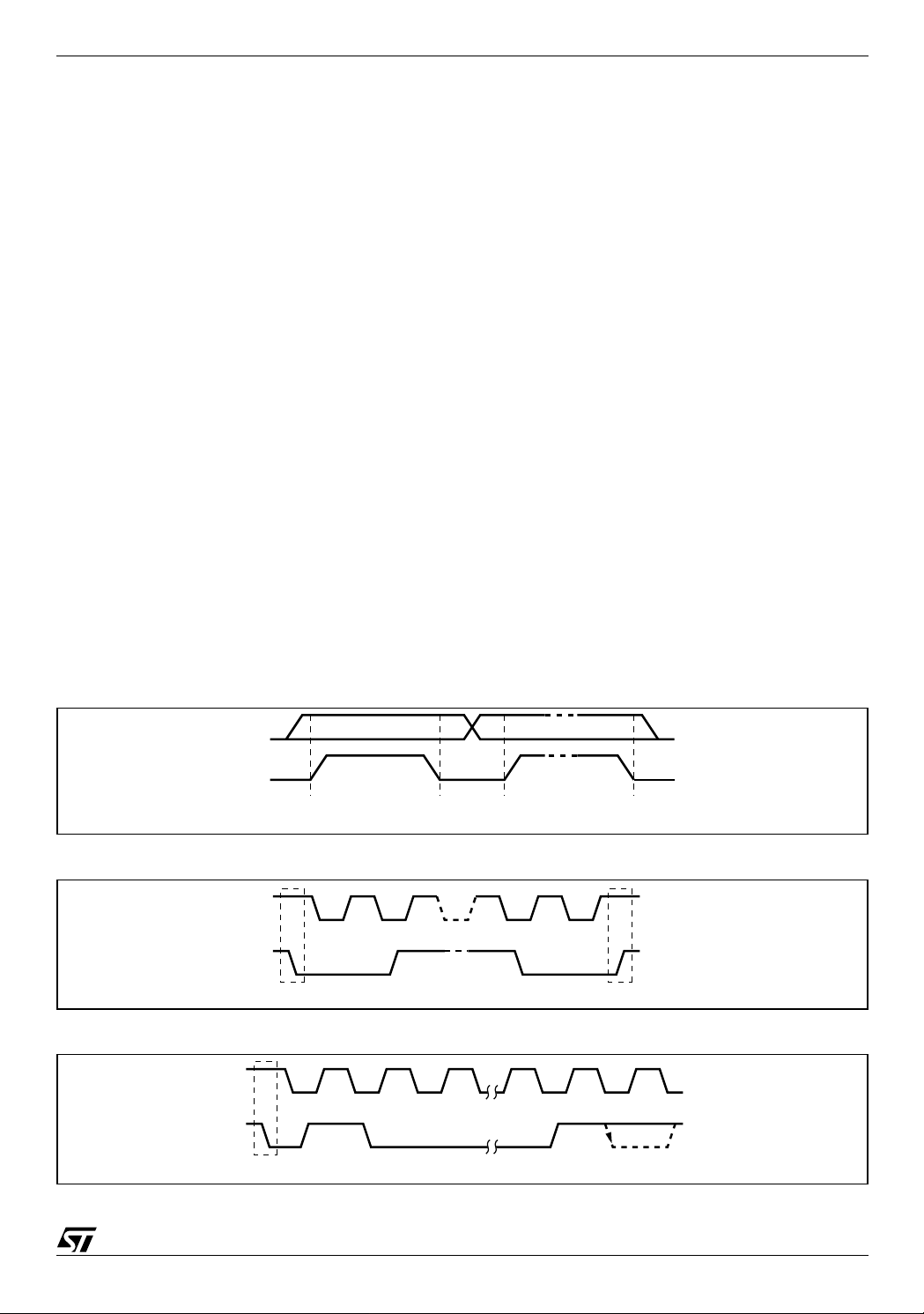
As shown in fig. 8, the data on the SDA line must be stable during the high period of the clock. The HIGH and
LOW state of the data line can only change when the clock signal on the SCL line is LOW.
4.2 Start and Stop Conditions
As shown in fig. 9 a start condition is a HIGH to LOW transition of the SDA line while SCL is HIGH. The stop
condition is a LOW to HIGH transition of the SDA line while SCL is HIGH.
4.3 Byte Format
Every byte transferred on the S DA l ine mus t contain 8 bits. Each byte must be followed by an acknowledge bit.
The MSB is transferred first.
4.4 Acknowledge
The master (µP) puts a resistive HIGH level on the SDA line during the acknowledge clock pulse (see fig. 10). The
peripheral (audio processor) that acknowledges has to pull-down (LOW) the SDA line during this clock pulse.
The audio processor which has been addressed has to generate an acknowledge after the reception of each
byte, otherwise the SDA li ne remains at the HIGH level dur ing the nin th clock pulse time. In thi s case the master
transmitter can generate the STOP information in order to abort the transfer.
4.5 Transmission without Acknowledge
Avoiding to detect the acknowledge of the audio processor, the µP can use a simpler transmission: simply it
waits one clock without checking the slave acknowledging, and sends the new data.
This approach of course is less protected from misworking.
Figure 8. Data Validity on the I2CBUS
SDA
SCL
2
Figure 9. Timing Diagram of I
SCL
SDA
CBUS
START
Figure 10. Acknowledge on the I
SCL
DATA LINE
STABLE, DATA
VALID
2
CBUS
1
CHANGE
DATA
ALLOWED
D99AU1032
23789
D99AU1031
STOP
2
I
CBUS
SDA
START
MSB
D99AU1033
ACKNOWLEDGMENT
FROM RECEIVER
5/14
 Loading...