

DIGITALLY CONTROLLED AUDIO PROCESSOR WITH
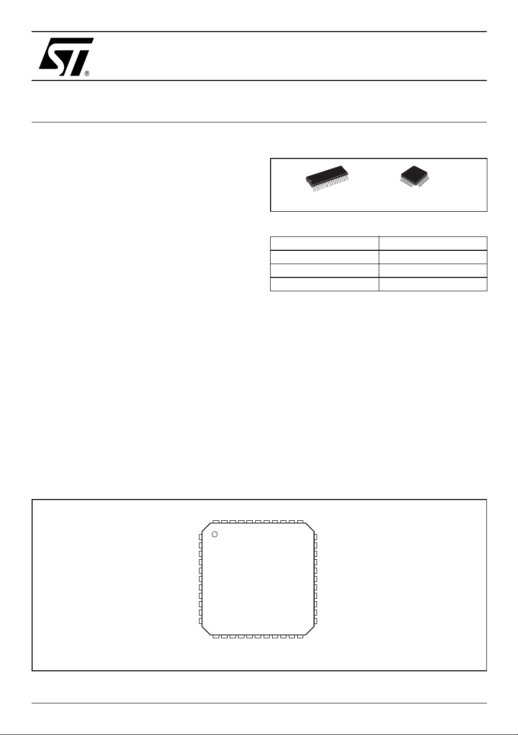
Figure 1. Package
T
SURROUND SOUND MATRIX AND VOICE CANCELLER
1FEATURES
■ 1 STEREO (4STEREO) IN PU T + 1 MIXER
INPUT
■ INPUT ATTENUATION CONTROL IN 0.5dB
STEP
■ VOICE CANCELLER IS AVAIL ABL E
■ TREBLE MIDDLE AND BASS CONTROL
■ THREE SURROUND MODES ARE
AVAILABLE
– MUSIC: 4 SELECTABLE RESPONSES
– MOVIE AND SIMULATED:
256 SELECTABLE RESPONSES
■ 2 SPEAKERS AND 2 RECORD
ATTENUATORS:
– 2 INDEPENDENT SPEAKERS AND 2 INDE-
PENDENT RECORD CONTROL
IN 1dB STEP FOR BALANCE FACILITY
– AVAILABIL ITY OF LO UDSPEA KER EQUAL -
IZATION FIXED BY EXTERNAL COMPONENTS
– INDEPENDENT MUTE FUNCTION
■ ALL FUNCTIONS PROGRAMMABLE VIA
SERIAL BUS
TDA7430
TDA7431
SDIP42 TQFP44
able 1. Order Codes
Part Number Package
TDA7431S SDIP42
TDA7430 TQFP44
TDA7430TR Tape & Reel
2 DESCRIPTION
The TDA7430/TDA7431 is volume tone (bass middle
and treble) balance (Left/Right) processors
canceller for quality audio applications in car radio
and Hi-Fi systems.
They reproduce surround sound by using programmable phase shifters and a signal matrix.
Control of all the functions is accomplished by serial bus. The AC signal setting is obtained by resistor networks and switches combined with
operational amplifiers. Thanks to the used BIPOLAR/CMOS Technology,
Low Distortion, Low Noise an d DC stepping are
obtained.
voice
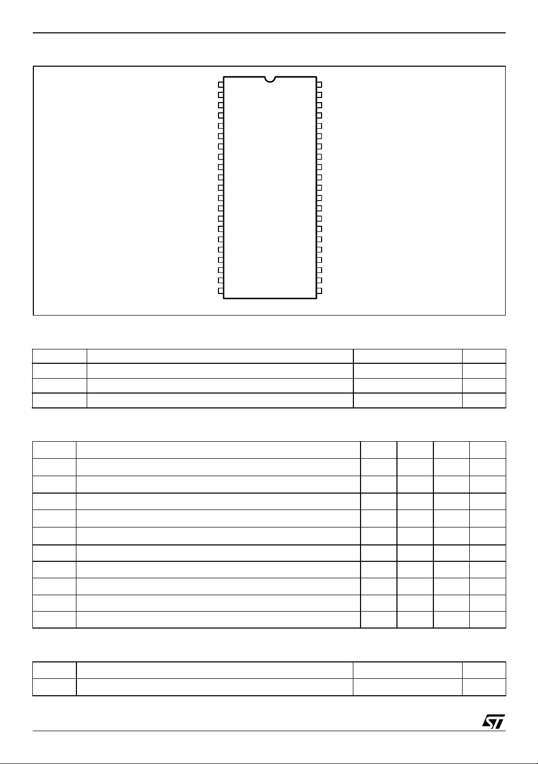
Figure 2. Pin Connection (TDA7430)
June 2004
HP2.
REAROUT
REARIN
VAR_L
BASSO_L
VAR_R
BASSO_R
BASS_LO
BASS_LI
LP
PS1
PS2
PS3
44 43 42 413940 38 37 36 35 34
1
LP1
2
HP1
3
4
5
6
7
8
9
10
12 13 14 15 16
BASS_RI
BASS_RO
MIDDLE_LI
MIDDLE_LO
S
PS4
CREF
R_IN4
V
171118 19 20 21 22
TREBLE_L
TREBLE_R
MIDDLE_RI
MIDDLE_RO
R_IN3
AGND
R_IN2
SDA
LPVC
SCL
33
32
31
30
29
28
27
26
25
24
23
D95AU220B
R_IN1
MIX
L_IN1
L_IN2
L_IN3
L_IN4
RECOUT_L
RECOUT_R
L_OUT
R_OUT
DIG_GND
REV. 10
1/23
TDA7430 - TDA7431
D95AU219B
Figure 3. Pin Connection (TDA7431)
VOUTREF
VAR_L
BASSO_L
VAR_R
BASSO_R
BASS_LO
BASS_LI
BASS_RO
BASS_RI
MIDDLE_LO
MIDDLE_LI
MIDDLE_RO
MIDDLE_RI
PS4
PS3
PS2
PS1
LP
LP1
HP1
HP2
42
1
2
3
4
5
6
7
8
9
10
11
12
13
14
15
16
17
18
19
20
21
V
S
41
CREF
40
NBRO
39
NBRIN
38 LPVC
R_IN37
MIX
36
L_IN
35
NBLIN
34
NBLO
33
RECOUT_L
32
RECOUT_R
31
L_OUT
30
R_OUT
29
DIG_GND28
SCL
27
SDA
26
ADDR
25
AGND
24
TREBLE_L
23
TREBLE_R
22
Table 2. Absolute Maximum Ratings
Symbol Parameter Value Unit
V
T
amb
T
stg
Operating Supply Voltage 11 V
S
Operating Ambient Temperature 0 to 70 °C
Storage Temperature Range -55 to 150 °C
Table 3. Quick Reference Data
Symbol Parameter Min. Typ. Max. Unit
V
V
THD Total Harmonic Distortion V = 0.1Vrms f = 1KHz 0.01 0.1 %
S/N Signal to Noise Ratio V
S
Supply Voltage 7 9 10.2 V
S
Max Input Signal Handling 2 V
CL
= 1Vrms (mode = OFF) 106 dB
out
Channel Separation f = 1KHz 90 dB
C
Treble Control (2dB step) -14 14 dB
Middle Control (2dB step) -14 14 dB
Bass Control (2dB step) -14 14 dB
Balance Control 1dB step (LCH, RCH) -79 0 dB
Mute Attenuation 100 dB
RMS
Table 4. Thermal Data
Symbol Parameter Value Unit
R
2/23
th j-pin
Thermal Resistance Junction-pins 85 °C/W
Figure 4. TEST CIRCUIT (TDA7430)
680nF
D95AU224B
TDA7430 - TDA7431
2.7K
2.7K
22nF
22nF
4.7nF
100nF
1.2nF
5.6nF
5.6nF
5.6nF
100nF
22nF
18nF
18nF
MIDDLE-LO
22nF
MIDDLE-RO
PS4
PS3
PS2
PS1
LP1
TREBLE-R
TREBLE-L
LPVC
MIDDLE-LI
MIDDLE-RI
D95AU225B
2.2µF
9
40
41
42
43
LP
44
1
18
19
34
14
15
16
17
RECOUT-L RECOUT-R L-OUT R-OUT
BASSO-LVAR-RBASSO-R
876
27 26 25 24 23 22 21
2.2µF
VAR-L
2.2µF
REARIN
REAROUT
45
TDA7430
DIG-GND SCL SDA
0.47µF
0.47µF
R-IN4
R-IN3
37 36 35
20
AGND
32
HP2
0.47µF
R-IN2
HP1
32
33
31
30
29
28
39
38
10
11
12
13
R-IN1
L-IN1
L-IN2
L-IN3
L-IN4
V
S
CREF
BASS-LO
BASS-LI
BASS-RO
BASS-RI
0.47µF
0.47µF
0.47µF
0.47µF
0.47µF
100nF10µF
22µF
220nF
100nF
100nF
5.6K
100nF
100nF
5.6K
1µF
MIX
Figure 5. TEST CIRCUIT (TDA7431)
2.2µF
22nF
22nF
4.7nF
100nF
1.2nF
5.6nF
5.6nF
5.6nF
100nF
22nF
18nF
2.7K
18nF
2.7K
MIDDLE-LO
22nF
MIDDLE-RO
MIDDLE-RI
PS4
PS3
PS2
PS1
LP1
TREBLE-R
TREBLE-L
LPVC
MIDDLE-LI
12 11 10 8 7 37 36 35
13
2
3
4
LP
5
6
22
23
38
18
19
20
21
32 31 30 29 28 27 26 25 24
9
VOUTREF RECOUT-L RECOUT-R L-OUT R-OUT
2.2µF
VAR-L
TDA7431
680nF
0.47µF
HP1
HP2BASSO-LVAR-RBASSO-R
1µF
R-IN
DIG-GND SCL SDA ADDR AGND
MIX
0.47µF
L-IN
V
S
421
100nF10µF
41
40
39
34
33
NBRO
NBRIN
NBLIN
NBLO
15K
15K
220nF
220nF
7.5K
220nF
220nF
7.5K
22µF
CREF
100nF
14
BASS-LO
100nF
15
BASS-LI
BASS-RO
16
5.6K
100nF
100nF
17
BASS-RI
5.6K
3/23
TDA7430 - TDA7431
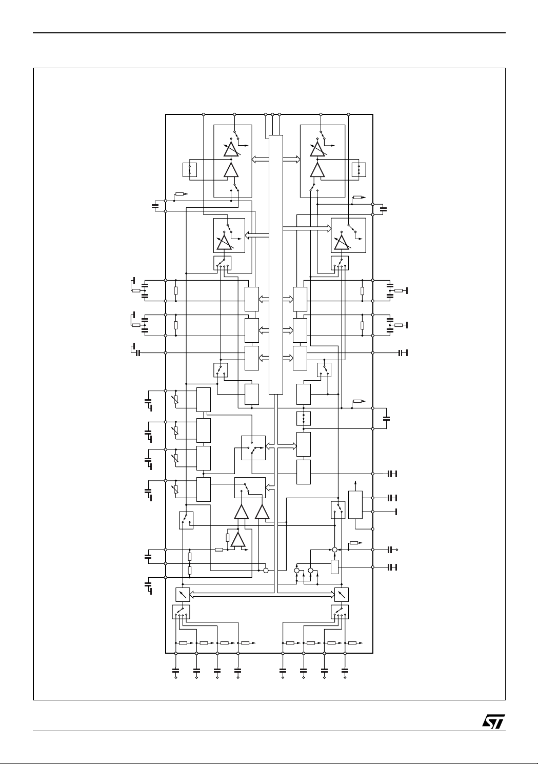
Figure 6. Block Diagram (TDA7430)
RECOUT-L
27
L-OUT
25
ATT
SPKR
79dB CONTROL
MUTE
SCL
SDA
222123
DIG GND
SPKR
R-OUT
RECOUT-R
24
26
ATT
MUTE
79dB CONTROL
D95AU221B
-
+
30K
2.2µF
BASSO-L VAR-L
79dB CONTROL
FIX
BASS-LO
100nF
5.6K
100nF
22nF
2.7K
18nF
5.6nF
10 7 6
RB
BASS-LI
MIDDLE-LO
RM
MIDDLE-LI
15 14 11
19
TREBLE-L
PS4
22nF
22nF
4.7nF
100nF
5.6nF 680nF
RPS4
41 40
PS3
RPS3
PS2
RPS2
PS1
RPS1
HP2
34342
2
1
LP1 HP1
31.5dB control
RHP1
RLP1
OFF
PS4
400Hz
PS3
400Hz
PS2
4KHz
PS1
90Hz
REC
SURR
R5
FIX
VAR
ATT
MUTE
3BAND
C BUS DECODER + LATCHES
2
BASS
MIDDLE
TREBLE
AMP
MIXING
MOVIE/SIM
MUSIC
MOVIE/
I
OFF
L-R
-
+
+
REAR
SURR
MUSIC
SIM
-
+
R6
-
+
+
FIX
FIX
MIDDLE BASS
TREBLE
AMP
MIXING
EFFECT
CONTROL
LPF
9KHz
-
+
30K
ATT
MUTE
SURR
RM RB
50K
Vref
SUPPLY
100K
31.5dB control
891218
2.2µF
BASSO-R VAR-R
79dB CONTROL
BASS-RO
BASS-RI
100nF 100nF
MIDDLE-RO
18nF 22nF
MIDDLE-RI
17 16 13
5.6nF
TREBLE-R
REARIN
2.2µF
REAROUT
45
1.2nF
LP
22µF
CREF
AGND
S
V
39 20 38 44
MIX
LPVC
1µF100nF
MIX-IN
3234
5.6K
2.7K
VAR
REC
3BAND
REAR
SURR
OFF
ON
VOICE
+LPF
-
4/23
50K
50K
50K
L-IN3
50K
28
L-IN4
0.47µF
31
30
29
L-IN2
L-IN1
0.47µF
0.47µF
0.47µF
50K
33
35
R-IN2
R-IN1
0.47µF
0.47µF
37
36
R-IN4
R-IN3
0.47µF
0.47µF
50K
50K
50K
THE SWITCHES POSITION MATCHES THE RESET CONDITION
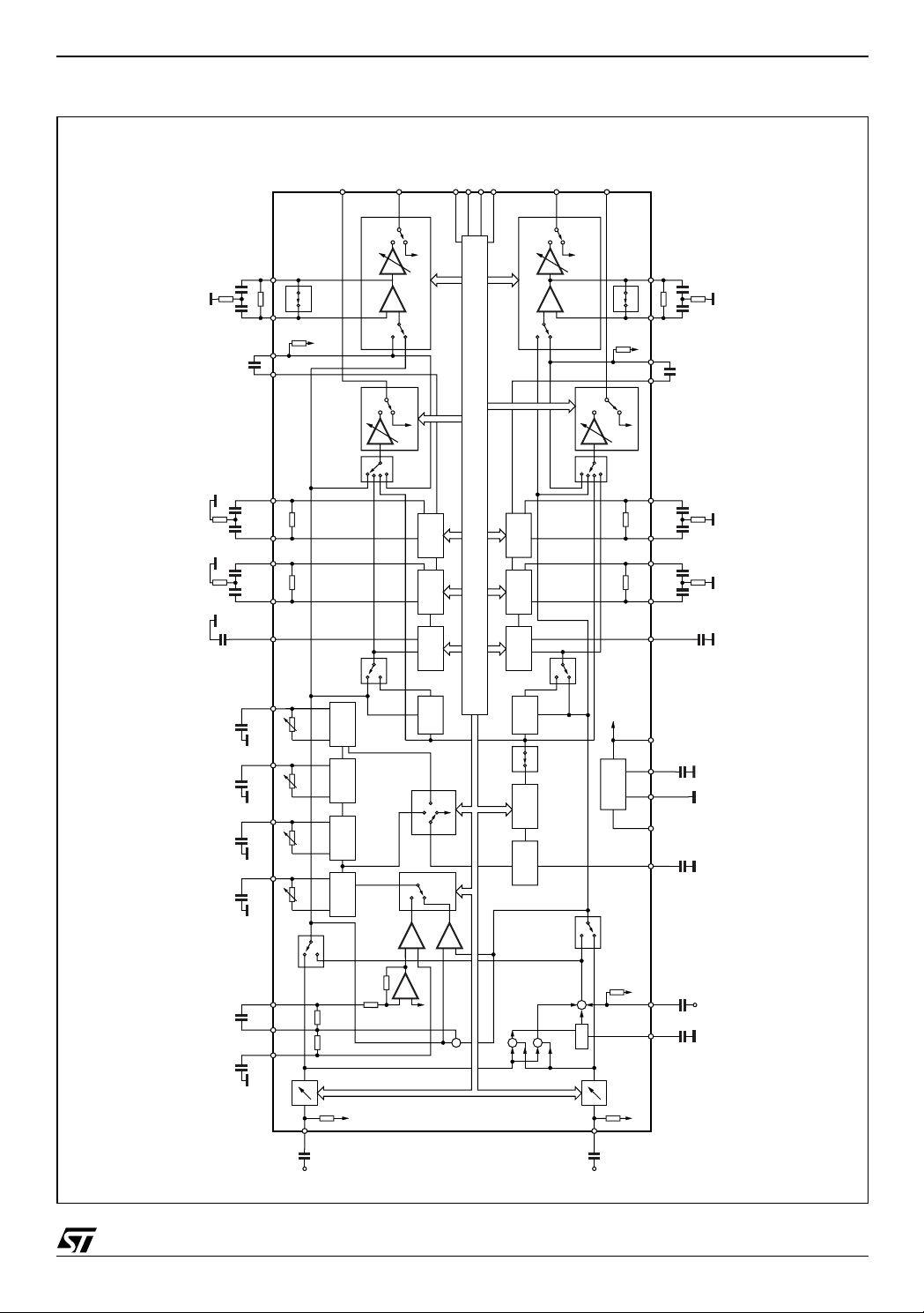
Figure 7. Block Diagram (TDA7431)
R
L
NBLO
NB2
NB1
NBLIN
NB-LA NB-LB
2.2µF
VAR-L
BASSO-L
30K
RECOUT-
32
79dB CONTROL
L-OUT
30
ATT
SPKR
79dB CONTROL
-
+
VAR
ATT
REC
MUTE
MUTE
FIX
SCL
SDA
272628
DIG GND
ADDR
25
TDA7430 - TDA7431
RECOUT-
R-OUT
29
31
30K
MUTE
D95AU222C
NBRO
40391213162293638
NB3
NBRIN
VAR-R
2.2µF
BASSO-R
79dB CONTROL
NB-RA NB-RB
NB4
ATT
SPKR
MUTE
79dB CONTROL
-
+
FIX
VAR
ATT
REC
5.6K
2.7K
100nF
100nF
22nF
18nF
5.6nF
22nF
22nF
4.7nF
100nF
5.6nF 680nF
FIX
BASS-LO
14 11 10 34 33
RB
BASS-LI
MIDDLE-LO
RM
MIDDLE-LI
19 18 15
23
TREBLE-L
PS4
RPS4
PS3
RPS3
PS2
RPS2
4321
PS1
RPS1
HP2
8
7
6
LP1 HP1
31.5dB control
35
L-in
0.47µF
RHP1
RLP1
50K
SURR
OFF
PS4
400Hz
PS3
400Hz
PS2
4KHz
PS1
90Hz
R5
3BAND
REAR
BASS
MIDDLE
TREBLE
SURR
AMP
MIXING
MOVIE/SIM
MUSIC
OFF
MUSIC
MOVIE/
SIM
L-R
-
-
+
+
R6
-
+
+
FIX
C BUS DECODER + LATCHES
2
I
MIDDLE BASS
TREBLE
SURR
AMP
MIXING
EFFECT
CONTROL
LPF
9KHz
-
+
3BAND
OFF
VOICE
BASS-RO
REAR
SURR
RM RB
21 20 17
Vref
SUPPLY
42 24 415
ON
100K
+LPF
control
31.5dB
50K
37
R-in
0.47µF
TREBLE-R
VOUTREF
CREF
AGND
S
V
LP
MIX
LPVC
5.6K
BASS-RI
100nF 100nF
MIDDLE-RO
2.7K
18nF 22nF
MIDDLE-RI
5.6nF
22µF
1.2nF
MIX-IN
1µF100nF
THE SWITCHES POSITION MATCHES THE RESET CONDITION
5/23
TDA7430 - TDA7431
Table 5. Electrical Characteristcs (refer to the te st circu it T
= 600Ω, all controls flat (G = 0dB), Effect CTRL = -6dB, MODE = OFF; f = 1KHz unless otherwise
R
G
= 25°C, VS = 9V, RL = 10KΩ, Vin = 1Vrms;
amb
specified).
Symbol Parameter Test Condition Min. Typ. Ma x. Unit
SUPPLY
V
SVR Ripple Rejection L
INPUT STAGE
R
V
C
RANGE
A
VMIN
A
VMAX
A
STEP
V
A
Supply Voltage 7 9 10.2 V
S
I
Supply Current 10 18 26 mA
S
/ R
CH
Input Resistance 35 50 65 KΩ
IN
Clipping Level THD = 0.3% 2 2.5 V
CL
, Mode = OFF 60 80 dB
CH out
Control Range 31.5 dB
Min. Attenuation -1 0 1 dB
Max. Attenuation 31 31.5 32 dB
Step Resolution 0.5 1 dB
DC Steps adjacent att. step -3 0 3 mV
DC
Voice Canceler Output 1 LIN = RIN, RIN = ON,
VO1
567dB
Vmix = 0V FIX, 0dB attenuation
rms
A
A
R
R
Voice Canceler Output 2 LIN = R
VO2
Voice Canceler Output 3 LIN = RIN, Vmix = 0V FIX,
VO3
Low Pass Filter Resistance 22.4 32 41.6 KΩ
LPV
Input Impedance 70 100 130 KΩ
MIX
BASS CONTROL
Control Range Max. Boost/cut ±11.5 ±14.0 ±16.0 dB
b
Step Resolution 1 2 3 dB
Internal Feedback Resistance 32 44 56 KΩ
B
B
G
STEP
R
MIDDLE CONTROL
Control Range Max. Boost/cut ±11.5 ±14.0 ±16.0 dB
m
Step Resolution 1 2 3 dB
Internal Feedback Resistance 17.5 25 32.5 KΩ
M
M
G
STEP
R
TREBLE CONTROL
G
Control Range Max. Boost/cut ±13.0 ±14.0 ±15.0 dB
t
T
STEP
Step Resolution 1 2 3 dB
= 0V,
IN
Vmix = 1V
FIX, 0dB attenuation
rms
0dB attenuation
-1 0 1 dB
567dB
6/23
TDA7430 - TDA7431
Table 5. Electrical Characteristcs (continued)
Symbol Parameter Test Condition Min. Typ. Ma x. Unit
EFFECT CONTROL
C
RANGE
S
STEP
Control Range ±13.0 6 dB
Step Resolution 0.5 1 1.5 dB
SURROUND SOUND MATRIX
TEST CONDITION (Phase Resistor Selection D0=0, D1=1, D2=0. D3=1, D4=0, D5=1, D6=0, D7=1
G
D
G
D
GMOV
G
D
L
MON1
OFF
GOFF
MOV
MUS
GMUS
In-phase Gain (OFF) Mode OFF, Input signal of 1kHz,
LR In-phase Gain Difference
(OFF)
1.4 V
, Rin → R
p-p
Mode OFF, Input signal of 1kHz,
1.4 V
, Rin → R
p-p
out , Lin
out , Lin
→ L
→ L
out
out
In-phase Gain (Movie) Movie mode, Effect Ctrl = -6dB
p-p
out , Lin
) - (Lin → L
out
,
→ L
out
out
p-p
)
LR In-phase Gain Difference
(Movie)
1kHz, 1.4 V
→ R
R
in
Movie mode, Effect Ctrl = -6dB
Input signal of 1kHz, 1.4 V
(Rin → R
In-phase Gain (Music) Music mode, Effect Ctrl = -6dB
LR In-phase Gain Difference
(Music)
Input signal of 1kHz, 1.4 V
(Rin → R
) , (Lin → L
out
Music mode, Effect Ctrl = -6dB
Input signal of 1kHz, 1.4 V
(Rin → R
) , (Lin → L
out
out
out
p-p
)
p-p
)
Simulated L Output 1 Simulated Mode, Effect Ctrl = -6dB
-1 0 1 dB
-1 0 1 dB
8dB
0dB
7dB
0dB
4.5 dB
Input signal of 250Hz,
L
MON2
1.4 V
, Rin and L
p-p
Simulated L Output 2 Simulated Mode, Effect Ctrl = -6dB
→ L
in
out
–4.0 dB
Input signal of 1kHz,
L
MON3
1.4 V
, Rin and L
p-p
Simulated L Output 3 Simulated Mode, Effect Ctrl = -6dB
→ L
in
out
7.0 dB
Input signal of 3.6kHz,
1.4 V
, Rin and L
p-p
→ L
in
out
R
R
R
R
R
R
MON1
MON2
MON3
LP1
HPI
LPF
Simulated R Output 1 Simulated Mode, Effect Ctrl = -6dB
– 4.5 dB
Input signal of 250Hz,
1.4 V
, Rin and L
p-p
Simulated R Output 2 Simulated Mode, Effect Ctrl = -6dB
→ R
in
out
3.8 dB
Input signal of 1kHz,
1.4 V
, Rin and L
p-p
Simulated R Output 3 Simulated Mode, Effect Ctrl = -6dB
→ R
in
out
– 20 dB
Input signal of 3.6kHz,
1.4 V
, Rin and L
p-p
→ R
in
out
Low Pass Filter Resistance 7 10 13 KΩ
High Pass Filter Resistance 42 60 78 KΩ
LP Pin Impedance 7 10 13 KΩ
7/23

TDA7430 - TDA7431
Table 5. Electrical Characteristcs (continued)
Symbol Parameter Test Condition Min. Typ. Ma x. Unit
SURROUBND SOUBND MATRIX PHASE
R
R
R
R
R
R
R
R
R
R
R
R
R
R
R
R
Phase Shifter 1: D1 = 0, D0 = 0 8.3 11.8 15.2 KΩ
PS10
Phase Shifter 1: D1 = 0, D0 = 1 10 14.1 18.3 KΩ
PS11
Phase Shifter 1: D1 = 1, D0 = 0 12.6 17.9 23.3 KΩ
PS12
Phase Shifter 1: D1 = 1, D0 = 1 26.4 37.3 48.85 KΩ
PS13
Phase Shifter 2: D3 = 0, D2 = 0 4 5.6 7.2 KΩ
PS20
Phase Shifter 2: D3 = 0, D2 = 1 4.8 6.8 8.7 KΩ
PS21
Phase Shifter 2: D3 = 1, D2 = 0 6 8.4 10.9 KΩ
PS22
Phase Shifter 2: D3 = 1, D2 = 1 12.9 18.3 23.7 KΩ
PS23
Phase Shifter 3: D5 = 0, D4 = 0 8.5 12.1 15.6 KΩ
PS30
Phase Shifter 3: D5 = 0, D4 = 1 10.2 14.5 18.7 KΩ
PS31
Phase Shifter 3: D5 = 1, D4 = 0 12.7 18.1 23.3 KΩ
PS32
Phase Shifter 3: D5 = 1, D4 = 1 27.4 39.1 50.75 KΩ
PS33
Phase Shifter 4: D7 = 0, D6 = 0 8.5 12.1 15.6 KΩ
PS40
Phase Shifter 4: D7 = 0, D6 = 1 10.2 14.5 18.7 KΩ
PS41
Phase Shifter 4: D7 = 1, D6 = 0 12.7 18.1 23.3 KΩ
PS42
Phase Shifter 4: D7 = 1, D6 = 1 27.4 39.1 50.75 KΩ
PS43
SPEAKER & RECORD ATTENUATORS
C
RANGE
S
STEP
E
V
A
MUTE
R
Control Range 79 dB
Step Resolution -0.5 1 1.5 dB
Attenuation set error Av = 0 to -20dB -1.5 0 1.5 dB
A
DC Steps adjacent att. steps -3 0 3 mV
DC
Output Mute Condition +70 100 dB
Input Impedance 21 30 39 KΩ
VEA
AUDIO OUTPUTS
N
O(OFF)
N
O(MOV)
N
O(Mus)
N
O(MON)
Output Noise (OFF) Output Mute, Flat
Output Noise (Movie) Mode = Movie
Output Noise (Music) Mode = Music
Output Noise (Simulated) Mode Simulated
8/23
A
= -20 to -79dB -3 0 2 dB
v
4
BW = 20Hz to 20KHz
5
30 µV
BW = 20Hz to 20KHz
30 µV
BW = 20Hz to 20KHz
30 µV
BW = 20Hz to 20KHz
µV
µV
rms
rms
rms
rms
rms

TDA7430 - TDA7431
Table 5. Electrical Characteristcs (continued)
Symbol Parameter Test Condition Min. Typ. Ma x. Unit
d Distorsion Av = 0 ; V
S
V
R
V
BUS INPUTS
V
V
V
Channel Separation 70 90 dB
C
Clipping Level d = 0.3% 2 2.5 Vrms
OCL
Output Resistance 10 40 70 Ω
OUT
DC Voltage Level 3.8 V
OUT
Input Low Voltage 1V
IL
Input High Voltage 3 V
IH
I
Input Current -5 +5 mA
IN
Output Voltage SDA
O
Acknowledge
IO = 1.6mA 0.4 V
in
= 1V
rms
0.01 0.1 %
3I2C BUS INTERFACE
Data transmission from microprocessor to the TDA7430/TDA7431 and viceversa takes place through the 2
2
wire s I
must be connected).
3.1 Data Validity
As shown in fig. 8, the data on the SDA line must be stable during the high period of the clock. The HIGH and
LOW state of the data line can only change when the clock signal on the SCL line is LOW.
C BUS interface, consisting of the tw o l ines SDA and SCL (pull- up res istors t o posi t ive suppl y voltage
3.2 Start and Stop Conditions
As shown in fig.9 a start condition is a HIGH to LOW transition of the SDA line while S CL is HIGH. The stop
condition is a LOW to HIGH transition of the SDA line while SCL is HIGH.
3.3 Byte Format
Every byte transferred on the SDA line must contain 8 bits. Each byte must be followed by an acknowledge bit.
The MSB is transferred first.
3.4 Acknowledge
The master (µP) puts a resistive HIGH level on the SDA line during the acknowledge clock pulse (see fig. 10).
The peripheral (audioprocessor) that acknowledges has to pull-down (LOW) the SDA line during this clock
pulse.
The audioprocessor which has been addressed has to generate an acknowledge after the recept ion of each
byte, otherwise the SDA line remains at the HIGH level during the ninth clock pulse time. In this case the master
transmitter can generate the STOP information in order to abort the transfer.
3.5 Tra nsmission wi th ou t Ack nowledge
Avoiding to detect the acknowledge of the audi oprocessor, the µP can use a simpler transmission: simply it
waits one clock without checking the slave acknowledging, and sends the new data.
This approach of course is less protected from misworking.
9/23

TDA7430 - TDA7431
S
S
S
S
S
S
S
T
D95AU226A
Figure 8. Data va l id ity on the I2C bus
DA
CL
DATA LINE
STABLE, DATA
2
Figure 9. Timin g D i agra m of I
C bus
CL
DA
START
Figure 10. Ack n owledge on th e I
CL
DA
START
1
MSB
CHANGE
DATA
VALID
2
C bus
ALLOWED
D99AU1032
D99AU1031
STOP
23789
D99AU1033
ACKNOWLEDGMEN
FROM RECEIVER
I
2
CBU
4 SOFTWARE SPECIFICATION
4.1 Interface Protocol
The interface protocol comprises:
■ A start condition (S)
■ A chip address byte, containing the TDA7430/TDA7431 address
■ A subaddress bytes
■ A sequence of data (N byte + achnowledge)
■ A stop condition (P)
Figure 11.
CHIP ADDRESS
MSB
S 1 0 0 0 0 0 A 0 ACK ACK DATA ACK P
10/23
LSB MSB LSB MSB LSB
SUBADDRESS DATA 1 to DATA n
B
DATA

TDA7430 - TDA7431
D95AU306
D95AU307
5 EXAMPLES
5.1 No Incremental Bus
The TDA7430/TDA7431 receives a start condition, the correct chip address, a subaddress with the MSB = 0 (no
incremental bus), N-datas (all these datas concern the subaddress selected), a stop condition.
Figure 12.
CHIP ADDRESS
MSB
S 1 0 0 0 0 0 A 0 ACK ACK DATA ACK P
LSB MSB LSB MSB LSB
SUBADDRESS DATA
X
X
D3
X
0
D2 D1 D0
5.2 Incremental B us
The TDA7430/TDA7431 receives a start condition, the correct chip address, a subaddress with the MSB = 1
(incremental bus): now it is in a loop condition with an autoincrease of the subaddress whereas SUBADDR ESS
from "1XXX1010" to "1XXX 1111" of DATA are ignored.The DA TA 1 concern thesubaddress sent, and the DATA
2 concern the subaddress sent plus one in the loop etc, and at the end it receivers the stop condition.
Figure 13.
CHIP ADDRESS
MSB
S 1 0 0 0 0 0 A 0 ACK ACK DATA ACK P
LSB MSB LSB MSB LSB
SUBADDRESS DATA 1 to DATA n
X
X
D3
X
1
D2 D1 D0
6 DATA BYTES
Address = 80(HEX) ADDR open; 82 (HEX): need to connect supply
6.1 Function Selection
Table 6. The first byte (Subaddress)
MSB LSB SUBADDRESS
D7 D6 D5 D4 D3 D2 D1 D0
B X X X 0 0 0 0 INPUT ATTENUATION
B X X X 0 0 0 1 SURROUND & OUT & EFFECT CONTROL
B X X X 0 0 1 0 PHASE RESISTOR
B X X X 0 0 1 1 BASS & NATURAL BASE
BXXX0100MIDDLE & TREBLE
B X X X 0 1 0 1 SPEAKER ATTENUATION "L"
B X X X 0 1 1 0 SPEAKER ATTENUATION "R"
BXXX0111AUX ATTENUATION "L"
BXXX1000AUX ATTENUATION"R"
B X X X 1 0 0 1 INPUT MULTIPLEXER, & AUX OUT
B = 1 incremental bus; active
B = 0 no incremental bus;
X = indifferen t 0, 1
11/23

TDA7430 - TDA7431
Table 7. INPUT ATTENUATION SELECTION
MSB LSB INPUT ATTENUATION
D7 D6 D5 D4 D3 D2 D1 D0 0.5 dB STEPS
X0000
X001-0.5
X010-1
X011-1.5
X100-2
X101-2.5
X110-3
X111-3.5
4 dB STEPS
X000 0
X001 -4
X010 -8
X011 -12
X100 -16
X101 -20
X110 -24
X111 -28
INPUT ATTE NUATION = 0 ~ -3 1.5dB
Table 8.
D7 D6 D5 D4 D3 D2 D1 D0 REAR SWITCH
X 0 REARIN, REAROUT PIN
ACTIVE
X 1 NO REARIN, REAROUT PIN
12/23

TDA7430 - TDA7431
Table 9. SURROUND SELECTION
MSB LSB
D7 D6 D5 D4 D3 D2 D1 D0 SURROUND MODE
00 SIMULATED
01 MUSIC
10 OFF
11 MOVIE
OUT
0VAR
1FIX
EFFECT CONTROL
0000 -6
0001 -7
0010 -8
0011 -9
0100 -10
0101 -11
0110 -12
0111 -13
1000 -14
1001 -15
1010 -16
1011 -17
1100 -18
1101 -19
1110 -20
1111 -21
Table 10. PHASE RESISTOR SELECTION
MSB LSB
D7 D6 D5 D4 D3 D2 D1 D0 PHASE SHIFT 1 (KΩ)
00 12
01 14
10 18
11 37
00 6
01 7
10 8
11 18
00 12
01 14
10 18
11 39
00 12
01 14
10 18
11 39
SURROUND PHAS E
RESISTOR
PHASE SHIFT 2 (KΩ)
PHASE SHIFT 3 (KΩ)
PHASE SHIFT 4 (KΩ)
13/23

TDA7430 - TDA7431
Table 11. BASS SELECTION
MSB LSB BASS
D7 D6 D5 D4 D3 D2 D1 D0 2 dB STEPS
0000 -14
0001 -12
0010 -10
0011 -8
0100 -6
0101 -4
0110 -2
0111 0
1111 0
1110 2
1101 4
1100 6
1011 8
1010 10
1001 12
1000 14
NATURAL BASE
0 NBRIN, NBRO, NBLIN,
1 NO NBRIN, NBRO, NBLIN,
NBLO PIN ACTIVE
NBLO PIN
Table 12. SPEAKER/AUX ATT. R & L SELECTION
MSB LSB SPEAKER/AUX ATT
D7 D6 D5 D4 D3 D2 D1 D0 1 dB STEPS
000 0
001 -1
010 -2
011 -3
100 -4
101 -5
110 -6
111 -7
8 dB STEPS
0000 0
0001 -8
0010 -16
0011 -24
0100 -32
0101 -40
0110 -48
0111 -56
1000 -64
1001 -72
MUTE
101X
11XX
X = INDIF F ERENT 0,1
SPEAKER/AUX ATTENUATION = 0dB ~ -79dB
14/23

TDA7430 - TDA7431
Table 13. MIDD LE & TREBLE SELECTION
MSB LSB MIDDLE
D7 D6 D5 D4 D3 D2 D1 D0 2 dB STEPS
0000 -14
0001 -12
0010 -10
0011 -8
0100 -6
0101 -4
0110 -2
0111 0
1111 0
1110 2
1101 4
1100 6
1011 8
1010 10
1001 12
1000 14
TREBLE
2 dB STEPS
0000 -14
0001 -12
0010 -10
0011 -8
0100 -6
0101 -4
0110 -2
0111 0
1111 0
1110 2
1101 4
1100 6
1011 8
1010 10
1001 12
1000 14
15/23

TDA7430 - TDA7431
D94AU204
D94AU198
Table 14. VOICE CANCELLER/INPUT/RECOUT L & R SELECTION
MSB LSB
D7 D6 D5 D4 D3 D2 D1 D0 VOICE CANCELER
010 OFF
001 ON
INPUT MULTIPLEXER
00 IN2
01 IN3
10 IN4
11 IN1
REC OUT "L"
0 0 VER 1 (3BAND)
0 1 VER 2 (SURR)
1 0 VER 3 (REAR)
11 FIX
REC OUT "R"
0 0 0 VER 1 (3BAND)
0 1 0 VER 2 (SURR)
1 0 0 VER 3 (REAR)
11 0 FIX
Table 15.
POWER ON RESET
BASS & MIDDLE 2dB
TREBLE 0dB
SURROUND & OUT CONTROL+ EFFECT CONTROL OFF + FIX + MAX ATTENUATION
SPEAKER/AUX ATTENUATION L &R MUTE
INPUT ATTENUATION + REAR SWITCH MAX ATTENUATION + ON
NATURAL BASE OFF
INPUT IN1
Figure 14. PINS: L-OUT, R-OUT, RECOUT-L,
Figure 15. PIN: HP1
RECOUT-R,
LP1
V
S
V
S
10K
20µA
100Ω
60K
GND
GND
HP2
16/23

TDA7430 - TDA7431
Vref
GND
REF
D94AU211
HP1
GND
GND
Figure 16. PIN: HP2
V
S
5.5K
60K
HP1
GND
D94AU199
Figure 17. PIN: VAR-L, VAR-R,
V
S
5.5K
20µA
20µA
Figure 19. PIN: LP 1
V
S
GND
Figure 20. PIN: CREF
V
S
20K
20µA
10K
20µA
SW
30K
D95AU227
Figu r e 1 8 . P IN: L-I N, R-IN, L-IN 2 , R-IN 2 , L- IN3,
R-IN3, L-IN4, R-IN4,
V
S
20µA
50K
GND
V
D94AU200
42K
20K
D95AU336
Figure 21. PIN: S C L, SDA
20µA
D94AU205
17/23

TDA7430 - TDA7431
D95AU308
GND GND
Vref
GND
Vref
GND
D95AU230
D95AU231A
BASS-RO,MIDDLE-LO,MIDDLE-RO
Figure 2 2. PIN: PS1, PS2, PS3, PS4, LP
V
S
20µA
GND
Figure 23. PIN: ADDR
V
S
20µA
Figure 25. PIN: M IX
V
S
20µA
100K
D94AU123
Figure 26. PINS: REAEROUT, BASSO-L,
BASSO-R
V
S
20µA
Figure 24. PIN: REARIN
V
S
SW
50K
50K
D95AU228A
20µA
D95AU229
GND
Figure 27. BASS-LI, BASS-RI, MIDDLE-L,
MIDDLE-RII
V
S
20µA
45K
GND
BASS-LO
or
25K
: Bass
: MIDDLE
18/23

TDA7430 - TDA7431
25K : MIDDLE
D95AU309
GND
Figure 28. PIN: BASS-LO, BASS-RO, MIDDLE-
LO, MIDDLE-RO,
V
S
20µA
(*)
GND
BASS-LI,BASS-RI,MIDDLE-LI,MIDDLE-RI
(*) 45K : Bass
D95AU232
Figure 29. PIN:TREBLE-L, TREBLE-R,
V
S
20µA
Figure 31. NBLIN, NBRIN
V
S
D95AU234
Figure 32. NBLO, NBRO
V
S
20µA
SWGND
25K
GND
Figure 30. PIN VOUT REF,
V
S
GND
10K
VREF
GND
D95AU235A
20µA
D95AU233A
19/23

TDA7430 - TDA7431
Figure 33. TQFP44 (10 x 10) Mechanical Data & Package Dimensions
DIM.
mm inch
MIN. TYP. MAX. MIN. TYP. MAX.
A 1.60 0.063
A1 0.05 0.15 0.002 0.006
A2 1.35 1.40 1.45 0.053 0.055 0.057
B 0.30 0.37 0.45 0.012 0.015 0.018
C 0.09 0.20 0.004 0.008
D 11.80 12.00 12.20 0.464 0.472 0.480
D1 9.80 10.00 10.20 0.386 0.394 0.401
D3 8.00 0.315
E 11.80 12.00 12.20 0.464 0.472 0.480
E1 9.80 10.00 10.20 0.386 0.394 0.401
E3 8.00 0.315
e 0.80 0.031
L 0.45 0.60 0.75 0.018 0.024 0.030
L1 1.00 0.039
k 0˚(min.), 3.5˚(typ.), 7˚(max.)
OUTLINE AND
MECHANICAL DATA
TQFP44 (10 x 10 x 1.4mm)
D
D1
33
34
B
44
1
e
23
11
TQFP4410
22
E
E1
12
L
Seating Plane
K
0.10mm
.004
A1
A
A2
B
C
0076922 D
20/23

Figure 34. SDIP42 Mechanical Data & Package Dimensions
TDA7430 - TDA7431
DIM.
mm inch
MIN. TYP. MAX. MIN. TYP. MAX.
A 5.08 0.20
A1 0.51 0.020
A2 3.05 3.81 4.57 0.120 0.150 0.180
B 0.38 0.46 0.56 0.0149 0.0181 0.0220
B1 0.89 1.02 1.14 0.035 0.040 0.045
c 0.23 0.25 0.38 0.0090 0.0098 0.0150
D 36.58 36.83 37.08 1.440 1.450 1.460
E 15.24 16.00 0.60 0.629
E1 12.70 13.72 14.48 0.50 0.540 0.570
e 1.778 0.070
e1 15.24 0.60
e2 18.54 0.730
e3 1.52 0.060
L 2.54 3.30 3.56 0.10 0.130 0.140
OUTLINE AND
MECHANICAL DATA
SDIP42 (0.600")
E
E1
A2
A1
LA
B eB1
D
42
1
22
21
c
SDIP42
e1
e2
E
.015
0,38
Gage Plane
e3
e2
21/23

TDA7430 - TDA7431
Table 16. Revision History
Date Revision Description of Changes
January 2004 9 First Issue in EDOCS DMS
June 2004 10 Changed the Style-sheet in compliance to the new “Corporate Technical
Pubblications Design Guide”
22/23

TDA7430 - TDA7431
Information furnished is believed to be accurate and reliable. However, STMicroelectronics assumes no responsibility for the consequences
of use of such information nor for any infringement of patents or other rights of third parties which may result from its use. No license is granted
by implic ation or oth erwise under any patent or patent rights of STMicroe l ectronics. Specificat i ons mentioned in thi s publication are subject
to change without notice. This publication supersedes and replaces all information previously supplied. STMicroelectronics products are not
authorized for use as critical comp onents in life support devi ces or systems wi t hout express written approval of STMi croelectr onics.
The ST logo is a register ed trademark of S T M i croelectroni cs.
All other nam es are the pro perty of their respectiv e owners
© 2004 STMi croelectro ni cs - All rights res erved
Australi a - Belgium - B razil - Canad a - China - Czech Republic - F i nl and - France - Germany - Hong Kong - India - Israel - Ital y - Japan -
Malaysia - Malta - Morocco - Singapore - Spain - Sweden - Switzerland - United Kingdom - United States
STMicroelectronics GROUP OF COMPANIES
www.st.com
23/23
 Loading...