

Features
■ Input Multiplexer
– QD: quasi-differential stereo inputs
– FD: full-differential stereo inputs
– Mono: Mono input
– SE1: stereo single-ended input
– SE2: stereo single-ended input
– In-Gain 0 to 15dB, 1dB step
– internal offset-cancellation (AutoZero)
■ IN/OUT control
– Selectable full-differential stereo inputs or
Bass output
■ Loudness
nd
–2
order frequency response
– programmable center frequency
(400Hz/800Hz/2400Hz)
– 15dB with 1dB steps
– soft-step control with programmable blend
times
– selectable low & high frequency boost
■ Volume
– +15dB to -79dB with 1dB step resolution
– soft-step control with programmable blend
times
– multi-step control
■ Bass
Table 1. Device summary
nd
–2
order frequency response
– center frequency programmable in 4 steps
(60Hz/80Hz/100Hz/200Hz)
– Q programmable 1.0/1.25/1.5/2.0
– DC gain programmable
– -15 to 15dB with 1dB resolution
– soft-step control with programmable blend
times
Order codes Package Packing
TDA7417 TQFP32 Tray
TDA7417TR TQFP32 Tape & reel
TDA7417
Car radio audio processor
TQFP32
■ Treble
– 2nd order frequency response
– center frequency programmable in 4 steps
(10KHz/12.5KHz/15KHz/17.5KHz)
– -15 to 15dB with 1dB resolution
■ High pass
– 2nd order frequency response
– center frequency programmable in 3 steps
(80Hz/120Hz/160Hz)
■ Speaker
– independent soft step speaker controls,
+15dB to -79dB with 1dB steps
– Independent programmable mix input with
50% mixing ratio for front speakers
–direct mute
– multi-step control
■ Mute Functions
– digitally controlled SoftMute with 3
programmable mute-times
(0.48ms/0.96ms/123ms)
Description
The TDA7417 is an high performance signal
processor specifically designed for car radio
applications with fully integrated audio filters.
The digital control allows a full programming of
the audioprocessor in a wide range of filter
characteristics.
By using BICMOS-process low distortion and low
noise are obtained.
June 2007 Rev 2 1/34
www.st.com
1

Contents TDA7417
Contents
1 Block diagram . . . . . . . . . . . . . . . . . . . . . . . . . . . . . . . . . . . . . . . . . . . . . . 6
2 Pins description . . . . . . . . . . . . . . . . . . . . . . . . . . . . . . . . . . . . . . . . . . . . 7
2.1 Pins description . . . . . . . . . . . . . . . . . . . . . . . . . . . . . . . . . . . . . . . . . . . . . 7
3 Electrical specifications . . . . . . . . . . . . . . . . . . . . . . . . . . . . . . . . . . . . . . 9
3.1 Thermal data . . . . . . . . . . . . . . . . . . . . . . . . . . . . . . . . . . . . . . . . . . . . . . . 9
3.2 Absolute maximum ratings . . . . . . . . . . . . . . . . . . . . . . . . . . . . . . . . . . . . . 9
3.3 Electrical characteristics . . . . . . . . . . . . . . . . . . . . . . . . . . . . . . . . . . . . . . . 9
4 Description of the audioprocessor . . . . . . . . . . . . . . . . . . . . . . . . . . . . 13
4.1 Input stages . . . . . . . . . . . . . . . . . . . . . . . . . . . . . . . . . . . . . . . . . . . . . . . 13
4.2 AutoZero . . . . . . . . . . . . . . . . . . . . . . . . . . . . . . . . . . . . . . . . . . . . . . . . . . 13
4.3 Loudness . . . . . . . . . . . . . . . . . . . . . . . . . . . . . . . . . . . . . . . . . . . . . . . . . 14
4.3.1 Attenuation . . . . . . . . . . . . . . . . . . . . . . . . . . . . . . . . . . . . . . . . . . . . . . . 14
4.3.2 Peak Frequency . . . . . . . . . . . . . . . . . . . . . . . . . . . . . . . . . . . . . . . . . . . 14
4.3.3 Low & high frequency boost . . . . . . . . . . . . . . . . . . . . . . . . . . . . . . . . . 15
4.3.4 Flat Mode . . . . . . . . . . . . . . . . . . . . . . . . . . . . . . . . . . . . . . . . . . . . . . . . 15
4.4 SoftMute . . . . . . . . . . . . . . . . . . . . . . . . . . . . . . . . . . . . . . . . . . . . . . . . . . 15
4.5 Multistep and Softstep Volume . . . . . . . . . . . . . . . . . . . . . . . . . . . . . . . . . 16
4.6 Bass . . . . . . . . . . . . . . . . . . . . . . . . . . . . . . . . . . . . . . . . . . . . . . . . . . . . . 17
4.6.1 Attenuation . . . . . . . . . . . . . . . . . . . . . . . . . . . . . . . . . . . . . . . . . . . . . . . 17
4.6.2 Center Frequency . . . . . . . . . . . . . . . . . . . . . . . . . . . . . . . . . . . . . . . . . 17
4.6.3 Quality Factors . . . . . . . . . . . . . . . . . . . . . . . . . . . . . . . . . . . . . . . . . . . . 18
4.6.4 DC Mode . . . . . . . . . . . . . . . . . . . . . . . . . . . . . . . . . . . . . . . . . . . . . . . . 18
4.7 Treble . . . . . . . . . . . . . . . . . . . . . . . . . . . . . . . . . . . . . . . . . . . . . . . . . . . . 19
4.7.1 Attenuation . . . . . . . . . . . . . . . . . . . . . . . . . . . . . . . . . . . . . . . . . . . . . . . 19
4.7.2 Center Frequency . . . . . . . . . . . . . . . . . . . . . . . . . . . . . . . . . . . . . . . . . 19
4.8 Highpass filter . . . . . . . . . . . . . . . . . . . . . . . . . . . . . . . . . . . . . . . . . . . . . . 20
4.9 Output Selector and Mixing . . . . . . . . . . . . . . . . . . . . . . . . . . . . . . . . . . . 20
4.10 IN/OUT control . . . . . . . . . . . . . . . . . . . . . . . . . . . . . . . . . . . . . . . . . . . . . 21
4.11 Audioprocessor Testing . . . . . . . . . . . . . . . . . . . . . . . . . . . . . . . . . . . . . . 21
4.12 Test circuit . . . . . . . . . . . . . . . . . . . . . . . . . . . . . . . . . . . . . . . . . . . . . . . . 22
2/34

TDA7417 Contents
5I
2
C Bus specification . . . . . . . . . . . . . . . . . . . . . . . . . . . . . . . . . . . . . . . 23
5.1 Interface Protocol . . . . . . . . . . . . . . . . . . . . . . . . . . . . . . . . . . . . . . . . . . . 23
5.1.1 Receive Mode . . . . . . . . . . . . . . . . . . . . . . . . . . . . . . . . . . . . . . . . . . . . 23
5.1.2 Transmission Mode . . . . . . . . . . . . . . . . . . . . . . . . . . . . . . . . . . . . . . . . 23
5.1.3 Reset Condition . . . . . . . . . . . . . . . . . . . . . . . . . . . . . . . . . . . . . . . . . . . 23
6 Serial data assign . . . . . . . . . . . . . . . . . . . . . . . . . . . . . . . . . . . . . . . . . . 24
6.1 Sub-address . . . . . . . . . . . . . . . . . . . . . . . . . . . . . . . . . . . . . . . . . . . . . . . 24
6.1.1 Main Source Selector (0) . . . . . . . . . . . . . . . . . . . . . . . . . . . . . . . . . . . . 25
6.1.2 Loudness (1) . . . . . . . . . . . . . . . . . . . . . . . . . . . . . . . . . . . . . . . . . . . . . 26
6.1.3 Volume/Mix volume/Fader LF/RF/LR/RR/SWL/SWR (2,8-14) . . . . . . . . 27
6.1.4 Softmute(3) . . . . . . . . . . . . . . . . . . . . . . . . . . . . . . . . . . . . . . . . . . . . . . 27
6.1.5 Treble(4) . . . . . . . . . . . . . . . . . . . . . . . . . . . . . . . . . . . . . . . . . . . . . . . . . 28
6.1.6 Bass(5) . . . . . . . . . . . . . . . . . . . . . . . . . . . . . . . . . . . . . . . . . . . . . . . . . 28
6.1.7 Highpass/Bass Frequency Control(6) . . . . . . . . . . . . . . . . . . . . . . . . . . 29
6.1.8 Smoother /In/Out Control(7) . . . . . . . . . . . . . . . . . . . . . . . . . . . . . . . . . 29
6.1.9 Fader Multistep Control(15) . . . . . . . . . . . . . . . . . . . . . . . . . . . . . . . . . . 30
6.1.10 Testing (16) . . . . . . . . . . . . . . . . . . . . . . . . . . . . . . . . . . . . . . . . . . . . . . 31
7 Package information . . . . . . . . . . . . . . . . . . . . . . . . . . . . . . . . . . . . . . . . 32
8 Revision history . . . . . . . . . . . . . . . . . . . . . . . . . . . . . . . . . . . . . . . . . . . 33
3/34

List of tables TDA7417
List of tables
Table 1. Device summary . . . . . . . . . . . . . . . . . . . . . . . . . . . . . . . . . . . . . . . . . . . . . . . . . . . . . . . . . . 1
Table 2. Pins description . . . . . . . . . . . . . . . . . . . . . . . . . . . . . . . . . . . . . . . . . . . . . . . . . . . . . . . . . . 7
Table 3. Thermal data. . . . . . . . . . . . . . . . . . . . . . . . . . . . . . . . . . . . . . . . . . . . . . . . . . . . . . . . . . . . . 9
Table 4. Absolute maximum ratings . . . . . . . . . . . . . . . . . . . . . . . . . . . . . . . . . . . . . . . . . . . . . . . . . . 9
Table 5. Electrical characteristics . . . . . . . . . . . . . . . . . . . . . . . . . . . . . . . . . . . . . . . . . . . . . . . . . . . . 9
Table 6. Registers of all subaddresses. . . . . . . . . . . . . . . . . . . . . . . . . . . . . . . . . . . . . . . . . . . . . . . 23
Table 7. Sub-address . . . . . . . . . . . . . . . . . . . . . . . . . . . . . . . . . . . . . . . . . . . . . . . . . . . . . . . . . . . . 24
Table 8. Main source selector (0) . . . . . . . . . . . . . . . . . . . . . . . . . . . . . . . . . . . . . . . . . . . . . . . . . . . 25
Table 9. Loudness (1) . . . . . . . . . . . . . . . . . . . . . . . . . . . . . . . . . . . . . . . . . . . . . . . . . . . . . . . . . . . . 26
Table 10. Volume/Mix volume/Fader LF/RF/LR/RR/SWL/SWR (2,8-14) . . . . . . . . . . . . . . . . . . . . . . 27
Table 11. Softmute(3) . . . . . . . . . . . . . . . . . . . . . . . . . . . . . . . . . . . . . . . . . . . . . . . . . . . . . . . . . . . . . 27
Table 12. Treble(4) . . . . . . . . . . . . . . . . . . . . . . . . . . . . . . . . . . . . . . . . . . . . . . . . . . . . . . . . . . . . . . . 28
Table 13. Bass(5) . . . . . . . . . . . . . . . . . . . . . . . . . . . . . . . . . . . . . . . . . . . . . . . . . . . . . . . . . . . . . . . . 28
Table 14. Highpass/Bass Frequency Control(6) . . . . . . . . . . . . . . . . . . . . . . . . . . . . . . . . . . . . . . . . . 29
Table 15. Smoother /In/Out Control(7) . . . . . . . . . . . . . . . . . . . . . . . . . . . . . . . . . . . . . . . . . . . . . . . . 29
Table 16. Fader Multistep Control(15) . . . . . . . . . . . . . . . . . . . . . . . . . . . . . . . . . . . . . . . . . . . . . . . . 30
Table 17. Testing (16). . . . . . . . . . . . . . . . . . . . . . . . . . . . . . . . . . . . . . . . . . . . . . . . . . . . . . . . . . . . . 31
Table 18. Document revision history . . . . . . . . . . . . . . . . . . . . . . . . . . . . . . . . . . . . . . . . . . . . . . . . . 33
4/34

TDA7417 List of figures
List of figures
Figure 1. Block diagram . . . . . . . . . . . . . . . . . . . . . . . . . . . . . . . . . . . . . . . . . . . . . . . . . . . . . . . . . . . . 6
Figure 2. Pins connection (Top view). . . . . . . . . . . . . . . . . . . . . . . . . . . . . . . . . . . . . . . . . . . . . . . . . . 7
Figure 3. Input stage . . . . . . . . . . . . . . . . . . . . . . . . . . . . . . . . . . . . . . . . . . . . . . . . . . . . . . . . . . . . . 13
Figure 4. Loudness Attenuation @ f
Figure 5. Loudness Center frequencies @ Attn. = 15dB . . . . . . . . . . . . . . . . . . . . . . . . . . . . . . . . . . 14
Figure 6. Loudness Attenuation, f
Figure 7. Softmute-Timing . . . . . . . . . . . . . . . . . . . . . . . . . . . . . . . . . . . . . . . . . . . . . . . . . . . . . . . . . 15
Figure 8. Soft Step and Multi Step timing . . . . . . . . . . . . . . . . . . . . . . . . . . . . . . . . . . . . . . . . . . . . . 16
Figure 9. Bass Control @ f
= 80Hz, Q = 1 . . . . . . . . . . . . . . . . . . . . . . . . . . . . . . . . . . . . . . . . . . . . 17
C
Figure 10. Bass center Frequencies @ Gain = 14dB, Q = 1 . . . . . . . . . . . . . . . . . . . . . . . . . . . . . . . . 17
Figure 11. Bass Quality factors @ Gain = 14dB, f
Figure 12. Bass normal and DC Mode @ Gain = 14dB, f
Figure 13. Treble Control @ f
= 17.5kHz . . . . . . . . . . . . . . . . . . . . . . . . . . . . . . . . . . . . . . . . . . . . . . 19
c
Figure 14. Treble Center Frequencies @ Gain = 14dB . . . . . . . . . . . . . . . . . . . . . . . . . . . . . . . . . . . . 19
Figure 15. Highpass Control . . . . . . . . . . . . . . . . . . . . . . . . . . . . . . . . . . . . . . . . . . . . . . . . . . . . . . . . 20
Figure 16. Output Selector . . . . . . . . . . . . . . . . . . . . . . . . . . . . . . . . . . . . . . . . . . . . . . . . . . . . . . . . . . 20
Figure 17. IN/OUT control . . . . . . . . . . . . . . . . . . . . . . . . . . . . . . . . . . . . . . . . . . . . . . . . . . . . . . . . . . 21
Figure 18. Test circuit . . . . . . . . . . . . . . . . . . . . . . . . . . . . . . . . . . . . . . . . . . . . . . . . . . . . . . . . . . . . . 22
Figure 19. TQFP32 Mechanical Data & Package Dimensions . . . . . . . . . . . . . . . . . . . . . . . . . . . . . . 32
= 400Hz . . . . . . . . . . . . . . . . . . . . . . . . . . . . . . . . . . . . . . . . . 14
P
=2.4kHz . . . . . . . . . . . . . . . . . . . . . . . . . . . . . . . . . . . . . . . . . . . . 15
c
= 80Hz. . . . . . . . . . . . . . . . . . . . . . . . . . . . . . . . . 18
C
= 80Hz . . . . . . . . . . . . . . . . . . . . . . . . . . . 18
c
5/34
Block diagram TDA7417
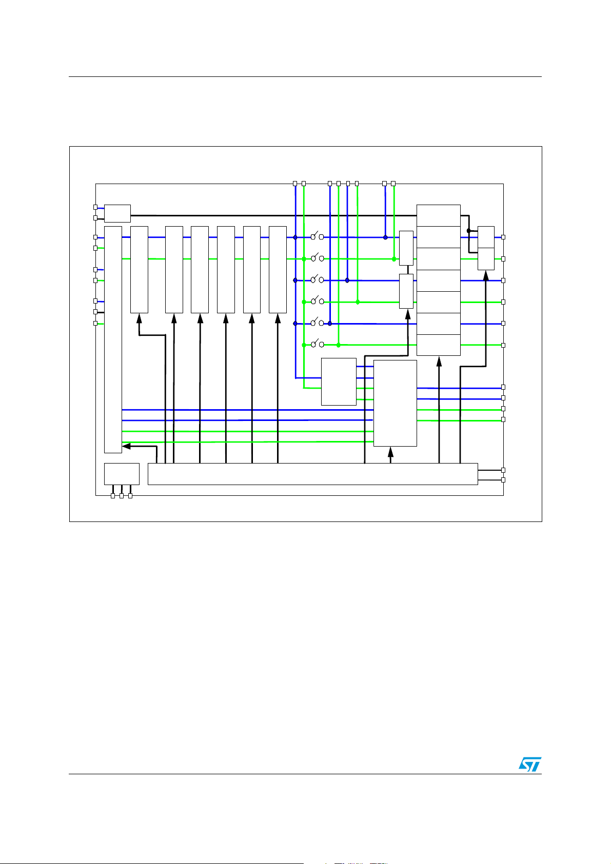
1 Block diagram
Figure 1. Block diagram
MonoDif
DifinG
SE1L
SE1R
SE2L
SE2R
DifinL
DifinG
DifinR
Mono
Diff
Input Multiplexer
Supply
ACOUTL
SWINL
ACOUTR
SWINR
LRIN
RRIN
RFIN
LFIN
Mixing
Volume
Mono Fader
HPFHPF
Mono Fader
Bass
Volume
Loudness
Treble
Softmute
Mono Fader
Mix
Mix
OutLF
OutRF
OutLR
Gain/Auto-Zero
Mono Fader
Mono Fader
Mono Fader
Balance
Amp
IN/OUT
SW
Digital Control I2C-Bus
OutRR
SW L
SW R
OUT/IN L+
OUT/IN L-
OUT/IN R+
OUT/IN R-
SCL
SDA
Vref
VCC
GND
6/34
TDA7417 Pins description
2 Pins description
Figure 2. Pins connection (Top view)
OUTSWL
OUTLR
323031 29 28 27 26 25
OUTLF
MonoDif
DifinG
OUTRF
OUTRR
OUTSWR
OUTINL-
OUTINL+
LFIN
LRIN
SWINL
ACOUTIL
SE1L
SE2L
1
2
3
4
5
6
7
8
910
Cref
VCC
11 12 13 14 15 16
SCL
SDA
GNDa
QDL
QDGND
QDR
24
23
22
21
20
19
18
17
D06AU1640
OUTINR-
OUTINR+
RFIN
RRIN
SWINR
ACOUTR
SE1R
SE2R
2.1 Pins description
Table 2. Pins description
NO. Pin Name Description I/O
1 OUTINL- Left- full-differential stereo input or bass differential output I/O
2 OUTINL+ Left+ full-differential stereo input or bass differential output I/O
3 LFIN Front AC coupling left input I
4 LRIN Rear AC coupling left input I
5 SWINL SW AC coupling left input I
6 ACOUTL AC coupling left output O
7 SE1L Single-ended input 1 left channel I
8 SE2L Single-ended input 2 left channel I
9 CREF Reference capacitor O
10 VCC Supply S
2
11 SDA I
12 SCL I
C bus data I/O
2
C bus clock I
13 GNDa Ground S
7/34
Pins description TDA7417
Table 2. Pins description (continued)
NO. Pin Name Description I/O
14 QDL Pseudo differential stereo input left I
15 QDGND Pseudo differential stereo input common I
16 QDR Pseudo differential stereo input right I
17 SE2R Single-ended input 2 right channel I
18 SE1R Single-ended input 1 right channel I
19 ACOUTR AC coupling right output O
20 SWINR SW AC coupling right input I
21 RRIN Rear AC coupling right input I
22 RFIN Front AC coupling right input I
23 OUTINR+ Right+ Full-differential stereo input or Bass differential output I/O
24 OUTINR- Right- Full-differential stereo input or Bass differential output I/O
25 OUTSWR SW right output O
26 OUTRR Rear right output O
27 OUTRF Front right output O
28 DifinG Mono differential input common I
29 MonoDif Mono differential input I
30 OUTLF Front left output O
31 OUTLR Rear left output O
32 OUTSWL SW left output O
8/34
TDA7417 Electrical specifications
3 Electrical specifications
3.1 Thermal data
Table 3. Thermal data
Symbol Description Value Unit
R
Thj-case
Thermal resistance junction-case 13 °C/W
3.2 Absolute maximum ratings
Table 4. Absolute maximum ratings
Symbol Parameter Value Unit
Operating supply voltage 9.5 V
Operating ambient temperature -40 to 85 °C
Storage temperature range -55 to 150 °C
ESD protection (Human Body Model) ±2000 V
ESD protection (Change Device Model) ±750 V
V
V
T
V
amb
T
S
stg
ESD
ESD
3.3 Electrical characteristics
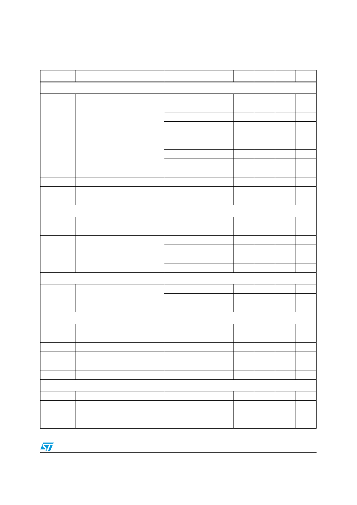
Table 5. Electrical characteristics
Symbol Parameter Test Condition Min. Typ. Max. Unit
SUPPLY
V
= 8.5V; T
S
= 25 C; RL= 10kΩ; all gains = 0dB; f = 1kHz; unless otherwise specified
amb
V
s
I
s
Supply voltage 8 8.5 9 V
Supply current 25 34 45 mA
INPUT SELECTOR
Rin Input resistance All single ended inputs 70 100 130 kΩ
V
G
IN MIN
G
IN MAX
G
V
V
CL
S
IN
STEP
DC
offset
Clipping level THD = 1% 2 2.3 V
Input separation 80 100 dB
Min. input gain -0.5 0 0.5 dB
Max. input gain 14.5 15 15.5 dB
Step resolution 0.5 1 1.5 dB
DC steps
Adjacent gain steps -5 1 5 mV
G
MIN to GMAX
-15 4 15 mV
Remaining offset with AutoZero 0.5 mV
9/34
RMS
Electrical specifications TDA7417
Table 5. Electrical characteristics (continued)
V
= 8.5V; T
S
Symbol Parameter Test Condition Min. Typ. Max. Unit
DIFFERENTIAL STEREO INPUTS
= 25 C; RL= 10kΩ; all gains = 0dB; f = 1kHz; unless otherwise specified
amb
R
in
Input resistance Differential 70 100 130 kΩ
CMRR Common mode rejection ratio
DIFFERENTIAL MONO INPUTS
R
in
Input resistance Differential 40 56 72 kΩ
CMRR Common mode rejection ratio
MIXING CONTROL
M
G
A
A
LEVEL
MAX
MAX
STEP
Mixing ratio Main / Mix Source -6/-6 dB
Max gain 131517dB
Max attenuation -83 -79 -75 dB
Step resolution 0.5 1 1.5 dB
LOUDNESS CONTROL
A
A
f
MAX
STEP
Peak
Max attenuation 14 15 16 dB
Step resolution 0.5 1 1.5 dB
Peak frequency
(1)
VOLUME CONTROL
V
CM=1 VRMS@ 1kHz
V
CM=1 VRMS@ 10kHz
V
=1 VRMS@ 1kHz 40 60 dB
CM
=1 VRMS@ 10kHz 40 60 dB
V
CM
f
P1
f
P2
f
P3
46 60 dB
46 60 dB
360 400 440 Hz
720 800 880 Hz
2200 2400 2600 Hz
G
A
A
V
MAX
MAX
STEP
E
A
E
T
DC
Max gain 141516dB
Max attenuation -83 -79 -75 dB
Step resolution 0.5 1 1.5 dB
Attenuation set error
G = -15to +15dB -1 0 1 dB
G = -79 to -15dB -4 0 3 dB
Tracking error 2dB
DC steps
Adjacent attenuation steps -3 0.1 3 mV
From 0dB to G
SOFT MUTE
A
MUTE
Mute attenuation 80 100 dB
T1 0.48 1 ms
T
D
Delay time
T2 0.96 2 ms
T3 70 123 170 ms
10/34
MIN
-7 0.5 7 mV
TDA7417 Electrical specifications
Table 5. Electrical characteristics (continued)
V
= 8.5V; T
S
Symbol Parameter Test Condition Min. Typ. Max. Unit
BASS CONTROL
= 25 C; RL= 10kΩ; all gains = 0dB; f = 1kHz; unless otherwise specified
amb
Fc Center frequency
Q
BASS
C
RANGE
A
STEP
DC
GAIN
Quality factor
Control range ±14 ±15 ±16 dB
Step resolution 0.5 1 1.5 dB
Bass-DC-gain
TREBLE CONTROL
C
RANGE
A
STEP
f
c
Control range ±14 ±15 ±16 dB
Step resolution 0.5 1 1.5 dB
Center frequency
HPF
(1)
(1)
(1)
f
C1
f
C2
f
C3
f
C4
Q
1
1.1 1.25 1.4
Q
2
54 60 66 Hz
72 80 88 Hz
90 100 110 Hz
180 200 220 Hz
0.9 1 1.1
Q3 1.3 1.5 1.7
Q4 1.8 2 2.2
DC = off -1 0 +1 dB
DC = on 3.5 4.4 5.5 dB
f
C1
f
C2
f
C3
f
C4
81012kHz
10 12.5 15 kHz
12 15 18 kHz
14 17.5 21 kHz
f
HP
Highpass corner frequency
SPEAKER ATTENUATORS
G
A
A
STEP
A
MUTE
E
V
MAX
MAX
E
DC
Max gain 141516dB
Max attenuation -83 -79 -75 dB
Step resolution 0.5 1 1.5 dB
Mute attenuation 80 90 dB
Attenuation set error 2 dB
DC steps Adjacent attenuation steps -5 0.1 5 mV
AUDIO OUTPUTS
Clipping level THD = 1% 2 2.3 V
Output impedance 5 30 100 W
Output load resistance 2 kΩ
Output load capacitor 10 nF
R
V
OUT
R
C
CL
L
L
(1)
f
HP1
f
HP2
f
HP3
72 80 88 Hz
108 120 132 Hz
144 160 176 Hz
11/34
RMS

Electrical specifications TDA7417
Table 5. Electrical characteristics (continued)
V
= 8.5V; T
S
Symbol Parameter Test Condition Min. Typ. Max. Unit
= 25 C; RL= 10kΩ; all gains = 0dB; f = 1kHz; unless otherwise specified
amb
V
DC
DC voltage level 4.05 4.25 4.4 V
AC COUPLING
R
ACIN
R
ACOUT
AC coupling input resistance 35 50 65 kΩ
AC coupling output resistance 5 50 100 Ω
IN/OUT CONTROL
R
in
CMRR Common mode rejection ratio
V
CL(IN)
V
CL(OUT)
R
OUT
R
IMPED
V
DC
Input resistance Differential 70 100 130 kΩ
VCM =1 VRMS@ 1kHz 40 60 dB
=1 VRMS@ 10kHz 40 60 dB
V
CM
In clipping level 1.9 2 V
Out clipping level 1.9 2 V
Output impedance 50 100 Ω
High impedance 200 kΩ
DC voltage level 3.1 3.3 3.5 V
I2C TIMING
VIH High input voltage for SDA,SCL 2.5 V
VIL Low input voltage for SDA,SCL 0.7 V
VOL Low output voltage for SDA 0.4 V
Tr SDA and SCL rise time 300 ns
Tf SDA and SCL fall time 300 ns
Tsdah SCL falling to SDA input hold time 0 0.9 us
Tsdas SDA input setup time to SCL rising 100 ns
RMS
RMS
GENERAL
BW=20Hz to 20 kHz all
e
NO
Output noise
gain = 0dB, HPF = off
BW=20Hz to 20 kHz
Output muted
S/N Signal to noise ratio
D Distortion
S
C
1. Min and max values are calculated according to simulation results; functionality is guaranteed by measuring a directly
correlated parameter
Channel separation left/right 80 90 dB
all gain = 0dB flat;
V
=2V
o
RMS
V
IN
=1V
RMS;
all stages
HPF = off
0dB
95 100 dB
12 25 µV
615µV
0.01 0.1 %
Note: It is not recommended that gain control and Softstep control be adjusted at the same time if
they are in the same byte.
It is not allowed to change multistep on/off or softstep on/off during the process of multistep
or softstep.
12/34

TDA7417 Description of the audioprocessor
4 Description of the audioprocessor
4.1 Input stages
In the basic configuration, one stereo quasi-differential, one selectable full-differential and
two single ended stereo inputs are available. As Figure 3 shown.
Quasi-differential stereo Input (QD)
The QD input is implemented as a buffered quasi-differential stereo stage with 100kΩ inputimpedance at each input. The attenuation is fixed to -3.5dB in order to adapt the incoming
signal level.
Single-ended stereo input (SE1, SE2)
The input-impedance at each input is 100kΩ and the attenuation is fixed to -3.5dB for
incoming signals.
Full differential stereo Input (FD)
The FD input is implemented as a selectable full-differential stereo stage with 50k inputimpedance at each input or high impedance status. The attenuation is fixed to -3.5dB in
order to adapt the incoming signal level.The high impedance status is 100kΩ
Figure 3. Input stage
Quasi-differential
Full-differential
4.2 AutoZero
The AutoZero allows a reduction of the number of pins as well as external components by
canceling any offset generated by or before the In-Gain-stage (Please notice that externally
generated offsets, e.g. generated through the leakage current of the coupling capacitors,
are not canceled).
The auto-zeroing is started every time the input source is changed and needs max. 0.32ms
for the alignment. To avoid audible clicks the Audio processor is muted before the loudness
stage during this time.
SEL1/SER1
InGain
SEL2/SER2
Mute
13/34

Description of the audioprocessor TDA7417
AutoZero-Remain
In some cases, for example if the µP is executing a refresh cycle of the IIC-Busprogramming, it is not useful to start a new AutoZero-action because no new source is
selected and an undesired mute would appear at the outputs. For such applications, it can
be switched in the AutoZero-Remain-Mode (Bit 6 of the subaddress-byte). If this bit is set
to high, the AutoZero will not be invoked and the old adjustment-value remains.
4.3 Loudness
There are four parameters programmable in the loudness stage:
4.3.1 Attenuation
Figure 4 shows the attenuation as a function of frequency at fP = 400Hz.
Figure 4. Loudness Attenuation @ f
4.3.2 Peak Frequency
Figure 5 shows the four possible peak-frequencies at 400, 800 and 2400Hz.
Figure 5. Loudness Center frequencies @ Attn. = 15dB
= 400Hz
P
14/34

TDA7417 Description of the audioprocessor
4.3.3 Low & high frequency boost
Figure 6 shows the different Loudness shapes in low & high frequency boost.
Figure 6. Loudness Attenuation, f
4.3.4 Flat Mode
In flat mode the loudness stage works as a 0dB to -15dB attenuator.
4.4 SoftMute
The digitally controlled Softmute stage allows muting/demuting the signal with a I2C-bus
programmable slope. The mute process can be activated by the I
realized in a special S-shaped curve to mute slow in the critical regions (see Figure 7).
=2.4kHz
c
2
C-bus. This slope is
Figure 7. Softmute-Timing
SOFT MUTE
+SIGNAL
REF
-SIGNAL
AC00061
Time
Note: Please notice that a started Mute-action is always terminated and could not be interrupted
by a change of the mute -signal
15/34

Description of the audioprocessor TDA7417
2
4.5 Multistep and Softstep Volume
When the volume-level is changed audible clicks could appear at the output. The root cause
of those clicks
could either be a DC-Offset before the volume-stage or the sudden change of the envelope
of the audio signal. With the Multistep and Softstep feature both kinds of clicks could be
reduced to a minimum and are no more audible. Multistep feature supports N dB change,
each step is 1dB;During 1dB transition, it will have 32 divisions if choosing softstep. The
blend-time from one step to the next is user selectable.
Figure 8. Soft Step and Multi Step timing
Soft Step (S.S.)
32 divisions1dB
Blend
Time
Multi Step (M.S.)
1dB
(2dB)
NdB
Blend
Time
Multi Soft Step (M.S.S.)
1dB 32 divisions
Blend
Time
NdB
AC0006
16/34

TDA7417 Description of the audioprocessor
4.6 Bass
There are four parameters programmable in the bass stage:
4.6.1 Attenuation
Figure 9 shows the attenuation as a function of frequency at a center frequency of 80Hz.
Figure 9. Bass Control @ f
4.6.2 Center Frequency
Figure 10 shows the eight possible center frequencies 60, 80, 100 and 200Hz.
Figure 10. Bass center Frequencies @ Gain = 14dB, Q = 1
= 80Hz, Q = 1
C
17/34

Description of the audioprocessor TDA7417
4.6.3 Quality Factors
Figure 11 shows the four possible quality factors 1, 1.25, 1.5 and 2.
Figure 11. Bass Quality factors @ Gain = 14dB, f
4.6.4 DC Mode
It is used for cut only for shelving filter. In this mode the DC-gain is increased by 4.4dB. In
addition the programmed center frequency and quality factor is decreased by 25% which
can be used to reach alternative center frequencies or quality factors. Figure 12 shows DC
mode.
Figure 12. Bass normal and DC Mode @ Gain = 14dB, f
= 80Hz
C
= 80Hz
c
Note: The center frequency, Q and DC-mode can be set fully independently.
18/34

TDA7417 Description of the audioprocessor
4.7 Treble
There are two parameters programmable in the treble stage:
4.7.1 Attenuation
Figure 13 shows the attenuation as a function of frequency at a center frequency of
17.5kHz.
Figure 13. Treble Control @ f
4.7.2 Center Frequency
Figure 14 shows the four possible center frequencies 10k, 12.5k, 15k and 17.5kHz.
Figure 14. Treble Center Frequencies @ Gain = 14dB
= 17.5kHz
c
19/34

Description of the audioprocessor TDA7417
4.8 Highpass filter
The highpass filter has 2 order filter characteristics with programmable cut-off frequency
(80/120/160Hz)
Figure 15. Highpass Control
4.9 Output Selector and Mixing
The output-selector allows different sources to connect to the front output. The setup of the
output selector is shown in Figure 16. A Mixing-stage is placed after the front speakerattenuator and can be set to mixing-mode.
In normal mode, switch (sw1) turns to down and main signal is directly outputted through
front pin. In the mixing mode, switch (sw1) turns up, mono differential signal and main signal
are mixed with ratio -6/-6dB. Having a full volume-attenuator for the mix-signal, the stage
offers a wide flexibility to adapt the mixing levels.
Figure 16. Output Selector
Mono
Differential
Mix_out
Main
20/34
Attenuator
Attenuator
Attenuator
Attenuator
-6/-6
dB
sw
1
Rear
SW

TDA7417 Description of the audioprocessor
4.10 IN/OUT control
IN/OUT control offers selectable full-differential stereo input or Bass output as figure15
shown. When used as full-differential input, bass buffer output is disabled, full-differential
input switch sw1(sw4) closes and sw2(sw3) closes. When used as bass output, fulldifferential input switch sw1(sw4) opens and sw2(sw3) still closes, single ended bass output
signal is converted to full differential output. IN/OUT control supports high impedance status
when bass buffer output is disabled, full-differential input switch sw1(sw4) opens and
sw2(sw3) closes.
Figure 17. IN/OUT control
Enable
BassOUTL
FDL
3.5dB
1
–1
-3.5dB
4.11 Audioprocessor Testing
In the test mode, which can be activated by setting bit D7 of the IIC subaddress byte and bit
D0 of the testing audioprocessor byte, several internal signals are available at the QDL pin.
In this mode, the input resistance of 100kOhm is disconnected from the pin. Internal signals
available for testing are listed in the data-byte specification. External clock can be available
at the SE1R pin.
+
D
1
-
+
D
1
-
sw1
+
-
sw2 50k
sw3
50k
sw4
50k
50k
OUT/INL+
OUT/INL-
AC00063
21/34

Description of the audioprocessor TDA7417
4.12 Test circuit
Figure 18. Test circuit
47μF 47μF 47μF 47μF 47μF 47μF
100nF 100nF
OUTSWL OUTSWLOUTSL OUTLF OUTRF OUTRRMonoDif DiffG
4.7μF
4.7μF
470nF
470nF
470nF
OUTINL-
OUTINL+
LFIN
LRIN
SWINL
2526272829303132
1
2
3
4
5
24
23
22
21
20
OUTINR-
OUTINR+
RFIN
RRIN
SWINR
4.7μF
4.7μF
470nF
470nF
470nF
100nF
100nF
ACOUTL
6
7
SE1L
8
910
SE2L
Cref
Vcc SDA SCL GNDa QDL QDRQDGND
10μF
10μF 100nF
1211 13 14 15 16
100nF
100nF10μF
19
18
17
ACOUTR
SE1R
SE2R
100nF
100nF
AC00064
22/34

TDA7417 I2C Bus specification
5 I2C Bus specification
5.1 Interface Protocol
The interface protocol comprises:
● a start condition (S)
● a chip address byte (the LSB determines read/write transmission)
● a subaddress byte
● a sequence of data (N-bytes + acknowledge)
● a stop condition (P)
● the max. clock speed is 500kbits/s
● 3.3V logic compatible
5.1.1 Receive Mode
S 1 0 0 0 1 0 0 R/W ACK TS AZ AI A4 A3 A2 A1 A0 ACK DATA ACK P
S = Start
R/W = "0" -> Receive Mode (Chip can be programmed by P)
"1" -> Transmission Mode (Data could be received by P)
ACK = Acknowledge
P = Stop
TS = Testing mode
AZ = Auto zero remain
AI = Auto increment
5.1.2 Transmission Mode
S1000100R/WACKXXXXXXXSMACKP
SM = Soft mute activated for main channel
X = Not Used
The transmitted data is automatic updated after each ACK. Transmission can be repeated
without new chip address.
5.1.3 Reset Condition
A Power-On-Reset is invoked if the Supply-Voltage is below than 3.5V. After that the
following data is written automatically into the registers of all subaddresses:
Table 6. Registers of all subaddresses
MSB LSB
111111 1 0
23/34

Serial data assign TDA7417
6 Serial data assign
6.1 Sub-address
Table 7. Sub-address
MSB LSB
I2 I1 I0 A4 A3 A2 A1 A0
0
1
0
1
0
1
0 0 0 0 0 Main Source Selector
0 0 0 0 1 Loudness
0 0 0 1 0 Primary Volume
0 0 0 1 1 Softmute/Clock Generator
0 0 1 0 0 Treble Control
0 0 1 0 1 Bass Control
0 0 1 1 0 Highpass/Bass Frequency control
0 0 1 1 1 Smoother/In/Out control
FUNCTION
Tes ting Mo de
off
on
AutoZero Remain
off
on
Auto Increment Mode
Off
On
0 1 0 0 0 Mix volume
0 1 0 0 1 Mono Fader LF
0 1 0 1 0 Mono Fader RF
0 1 0 1 1 Mono Fader LR
0 1 1 0 0 Mono Fader RR
0 1 1 0 1 Mono Fader SWL
0 1 1 1 0 Mono Fader SWR
0 1 1 1 1 Fader Multistep control
1 0 0 0 0 Test control
24/34

TDA7417 Serial data assign
6.1.1 Main Source Selector (0)
Table 8. Main source selector (0)
MSB LSB
D7 D6 D5 D4 D3 D2 D1 D0
0
0
0
0
1
0
0
0
0
0
0
0
0
1
1
1
1
1
1
1
1
0
0
0
0
1
1
1
1
0
0
0
0
1
1
1
1
0
0
1
1
0
0
1
1
0
0
1
1
0
0
1
1
0
1
0
1
0
1
0
1
0
1
0
1
0
1
0
1
0
0
1
1
X
Source Selector
0
QD
1
SE1
0
SE2
1
FD
X
Mute
Input Gain
0dB
1dB
2.dB
3dB
4dB
5dB
6dB
7dB
8dB
9dB
10dB
11dB
12dB
13dB
14dB
15dB
FUNCTION
Auto Zero
0
1
on
off
25/34

Serial data assign TDA7417
6.1.2 Loudness (1)
Table 9. Loudness (1)
MSB LSB
D7 D6 D5 D4 D3 D2 D1 D0
0
0
0
0
0
0
0
0
1
1
1
1
1
1
1
1
0
0
1
1
0
1
0
1
0
0
0
0
1
1
1
1
0
0
0
0
1
1
1
1
0
0
1
1
0
0
1
1
0
0
1
1
0
0
1
1
0
1
Attenuation
0
0dB
1
-1dB
0
-2.dB
1
-3dB
0
-4dB
1
-5dB
0
-6dB
1
-7dB
0
-8dB
1
-9dB
0
-10dB
1
-11dB
0
-12dB
1
-13dB
0
-14dB
1
-15dB
Center Frequency
Flat
400Hz
800Hz
2400Hz
High Boost
on
off
FUNCTION
0
1
26/34
Softstep
on
off

TDA7417 Serial data assign
6.1.3 Volume/Mix volume/Fader LF/RF/LR/RR/SWL/SWR (2,8-14)
Table 10. Volume/Mix volume/Fader LF/RF/LR/RR/SWL/SWR (2,8-14)
MSB LSB
D7 D6 D5 D4 D3 D2 D1 D0
Gain/Attenuation
0
0
0
0
0
0
1
1
1
0
0
0
:
:
0
0
0
:
:
0
0
1
0
0
0
:
0
1
1
:
1
1
x
0
0
0
1
0
0
1
1
x
0
0
0
:
1
0
0
:
1
1
x
0
0
0dB
0
1
1dB
1
0
2.dB
:
:
:
:
:
1
1
15dB
0
0
-0dB
0
1
-1dB
:
:
:
1
0
-78dB
1
1
-79dB
x
x
mute
Softstep
0
1
on
off
6.1.4 Softmute(3)
FUNCTION
Table 11. Softmute(3)
MSB LSB
D7 D6 D5 D4 D3 D2 D1 D0
Soft Mute
0
on
1
off
Soft Mute Time
0
0
1
0
1
x
0.48ms
0.96ms
123ms
Softstep Time
0
0
0
0
1
1
1
1
0
0
1
1
0
0
1
1
0
1
0
1
0
1
0
1
0.160ms
0.321ms
0.642ms
1.28ms
2.56ms
5.12ms
10.24ms
20.48ms
x Not used
x Not used
FUNCTION
27/34

Serial data assign TDA7417
6.1.5 Treble(4)
Table 12. Treble(4)
MSB LSB
D7 D6 D5 D4 D3 D2 D1 D0
0
1
FUNCTION
Gain/Attenuation
0
0
:
0
0
1
1
:
1
1
1
1
0
0
0
0
1
1
1
1
:
0
0
0
0
:
1
1
1
1
-15dB
1
0
-14dB
:
:
:
:
:
0
1
-1dB
0
0
0dB
0
0
0dB
0
1
+1dB
:
:
:
1
0
+14dB
1
1
+15dB
Treble Center Frequency
0
0
1
1
0
1
0
1
10kHz
12.5kHz
15kHz
17.5kHz
Volume Multistep Control
on
off
6.1.6 Bass(5)
Table 13. Bass(5)
MSB LSB
D7 D6 D5 D4 D3 D2 D1 D0
0
1
0
0
:
0
0
1
1
:
1
1
0
0
1
1
0
1
0
1
1
1
0
0
0
0
1
1
1
1
:
0
0
0
0
:
1
1
1
1
:
:
0
0
0
0
:
:
1
1
Gain/Attenuation
1
-15dB
0
-14dB
:
:
1
-1dB
0
0dB
0
0dB
1
+1dB
:
:
0
+14dB
1
+15dB
Bass Q Factor
1
1.25
1.5
2
Softstep Control
on
off
FUNCTION
28/34

TDA7417 Serial data assign
6.1.7 Highpass/Bass Frequency Control(6)
Table 14. Highpass/Bass Frequency Control(6)
MSB LSB
D7 D6 D5 D4 D3 D2 D1 D0
x Not used
FUNCTION
Bass Frequency
0
0
60Hz
0
1
80Hz
1
0
100Hz
1
1
200Hz
Bass DC Mode
0
1
on
off
Front Highpass Frequency
0
0
1
0
1
x
80Hz
120Hz
160Hz
Rear Highpass Frequency
0
0
1
0
1
x
80Hz
120Hz
160Hz
6.1.8 Smoother /In/Out Control(7)
Table 15. Smoother /In/Out Control(7)
MSB LSB
D7 D6 D5 D4 D3 D2 D1 D0
x Not used
Mixing Enable
0
on
1
off
Smoother Filter
0
1
on
off
AC coupling
0
1
on
off
In Out Control
0
0
1
0
1
x
in
out
High Impedance
Front Highpass Control
0
1
on
bypass
Rear Highpass Control
0
1
on
bypass
FUNCTION
29/34

Serial data assign TDA7417
6.1.9 Fader Multistep Control(15)
Table 16. Fader Multistep Control(15)
MSB LSB
D7 D6 D5 D4 D3 D2 D1 D0
0
1
0
1
0
1
0
1
0
1
0
1
Fader LF Multistep
0
on
1
off
Fader RF Multistep
on
off
Fader LR Multistep
on
off
Fader RR Multistep
on
off
Fader SWL Multistep
on
off
Fader SWR Multistep
on
off
Mixing to Left Front Speaker
on
off
FUNCTION
0
1
30/34
Mixing to Right Front Speaker
on
off

TDA7417 Serial data assign
6.1.10 Testing (16)
Table 17. Testing (16)
MSB LSB
D7 D6 D5 D4 D3 D2 D1 D0
0
0
0
0
0
0
0
0
1
1
1
1
1
1
1
0
0
0
0
1
1
1
1
0
0
0
0
1
1
1
0
0
1
1
0
0
1
1
0
0
1
1
0
0
1
0
1
0
1
0
1
0
1
0
1
0
1
0
1
0
0
1
FUNCTION
Audio Processor Testing Mode
0
off
1
on
Test Multiplexer
Right Bass opmos2 out
Right Bass Vref
Left InGain
Right Bass opmos21 out
Left Volume
Left Loudness
Left Bass
Left Treble
REF5.5V
Left Highpass out
1.95V
VBG 1.26V
SSCLK
CLK200
SMCLK
Clock Source
external
internal
Clock Fast Mode
0
1
on
off
x Not used
31/34

Package information TDA7417
7 Package information
In order to meet environmental requirements, ST offers these devices in ECOPACK®
packages. These packages have a Lead-free second level interconnect. The category of
second Level Interconnect is marked on the package and on the inner box label, in
compliance with JEDEC Standard JESD97. The maximum ratings related to soldering
conditions are also marked on the inner box label. ECOPACK is an ST trademark.
ECOPACK specifications are available at: www.st.com.
Figure 19. TQFP32 Mechanical Data & Package Dimensions
DIM.
A 1.60 0.063
A1 0.05 0.15 0.002 0.006
A2 1.35 1.40 1.45 0.053 0.055 0.057
B 0.30 0.37 0.45 0.012 0.015 0.018
C 0 .09 0.20 0.004 0.008
D 9.00 0.354
D1 7.0 0 0 .276
D3 5.6 0 0 .220
e 0.80 0.031
E 9.00 0.354
E1 7.00 0.276
E3 5.60 0.220
L 0.45 0.60 0.75 0.018 0.024 0.030
L1 1.00 0.039
K 0˚(min.), 3.5°(typ.), 7°(max.)
mm inch
MIN. TYP. MAX. MIN. TYP. MAX.
D
D1
OUTLINE AND
MECHANICAL DATA
Weight: 0.20gr
TQFP32 (7 x 7 x 1.40mm)
A1
A
A2
1724
25
B
32
1
e
16
9
8
TQFP32
32/34
E3D3E1
0.10mm
.004
Seating Plane
E
L1
L
K
B
C
0060661 C

TDA7417 Revision history
8 Revision history
Table 18. Document revision history
Date Revision Changes
28-Feb-2007 1 Initial release.
26-Jun-2007 2 Corrected typo errors.
33/34

TDA7417
Please Read Carefully:
Information in this document is provided solely in connection with ST products. STMicroelectronics NV and its subsidiaries (“ST”) reserve the
right to make changes, corrections, modifications or improvements, to this document, and the products and services described herein at any
time, without notice.
All ST products are sold pursuant to ST’s terms and conditions of sale.
Purchasers are solely responsible for the choice, selection and use of the ST products and services described herein, and ST assumes no
liability whatsoever relating to the choice, selection or use of the ST products and services described herein.
No license, express or implied, by estoppel or otherwise, to any intellectual property rights is granted under this document. If any part of this
document refers to any third party products or services it shall not be deemed a license grant by ST for the use of such third party products
or services, or any intellectual property contained therein or considered as a warranty covering the use in any manner whatsoever of such
third party products or services or any intellectual property contained therein.
UNLESS OTHERWISE SET FORTH IN ST’S TERMS AND CONDITIONS OF SALE ST DISCLAIMS ANY EXPRESS OR IMPLIED
WARRANTY WITH RESPECT TO THE USE AND/OR SALE OF ST PRODUCTS INCLUDING WITHOUT LIMITATION IMPLIED
WARRANTIES OF MERCHANTABILITY, FITNESS FOR A PARTICULAR PURPOSE (AND THEIR EQUIVALENTS UNDER THE LAWS
OF ANY JURISDICTION), OR INFRINGEMENT OF ANY PATENT, COPYRIGHT OR OTHER INTELLECTUAL PROPERTY RIGHT.
UNLESS EXPRESSLY APPROVED IN WRITING BY AN AUTHORIZED ST REPRESENTATIVE, ST PRODUCTS ARE NOT
RECOMMENDED, AUTHORIZED OR WARRANTED FOR USE IN MILITARY, AIR CRAFT, SPACE, LIFE SAVING, OR LIFE SUSTAINING
APPLICATIONS, NOR IN PRODUCTS OR SYSTEMS WHERE FAILURE OR MALFUNCTION MAY RESULT IN PERSONAL INJURY,
DEATH, OR SEVERE PROPERTY OR ENVIRONMENTAL DAMAGE. ST PRODUCTS WHICH ARE NOT SPECIFIED AS "AUTOMOTIVE
GRADE" MAY ONLY BE USED IN AUTOMOTIVE APPLICATIONS AT USER’S OWN RISK.
Resale of ST products with provisions different from the statements and/or technical features set forth in this document shall immediately void
any warranty granted by ST for the ST product or service described herein and shall not create or extend in any manner whatsoever, any
liability of ST.
ST and the ST logo are trademarks or registered trademarks of ST in various countries.
Information in this document supersedes and replaces all information previously supplied.
The ST logo is a registered trademark of STMicroelectronics. All other names are the property of their respective owners.
© 2007 STMicroelectronics - All rights reserved
STMicroelectronics group of companies
Australia - Belgium - Brazil - Canada - China - Czech Republic - Finland - France - Germany - Hong Kong - India - Israel - Italy - Japan -
Malaysia - Malta - Morocco - Singapore - Spain - Sweden - Switzerland - United Kingdom - United States of America
www.st.com
34/34
 Loading...