

ST TDA7391 User Manual
35W BRIDGECAR RADIO AMPLIFIER
HIGHPOWER CAPABILITY:
40W/4Ω MAX
35W/4Ω EIAJ
45W/3.2Ω MAX
40W/3.2ΩEIAJ
32W/3.2Ω@V
26W/4Ω @V
DIFFERENTIAL INPUTS (EITHER SINGLE
ENDED OR DIFFERENTIAL INPUT SIGNAL
ARE ACCEPTED)
MINIMUMEXTERNALCOMPONENTCOUNT:
- NOBOOTSTRAPCAPACITORS
- NOBOUCHEROT CELLS
- INTERNALLYFIXEDGAIN(30dB)
- NOSVRCAPACITOR
ST.-BYFUNCTION (CMOS COMPATIBLE)
PROGRAMMABLETURN-ON/OFF DELAY
NO AUDIBLE POP DURING MUTE AND ST-
BY OPERATIONS
PROTECTIONS:
SHORT CIRCUIT (TO GND, TO V
THE LOAD)
VERYINDUCTIVE LOADS
CHIP OVERTEMPERATURE
LOADDUMP
OPENGND
S =14.4V,f = 1KHz,d = 10%
S= 14.4V, f = 1KHz, d =10%
ACROSS
S,
TDA7391
Multiwatt11
ORDERING NUMBER: TDA7391
ESD
DESCRIPTION
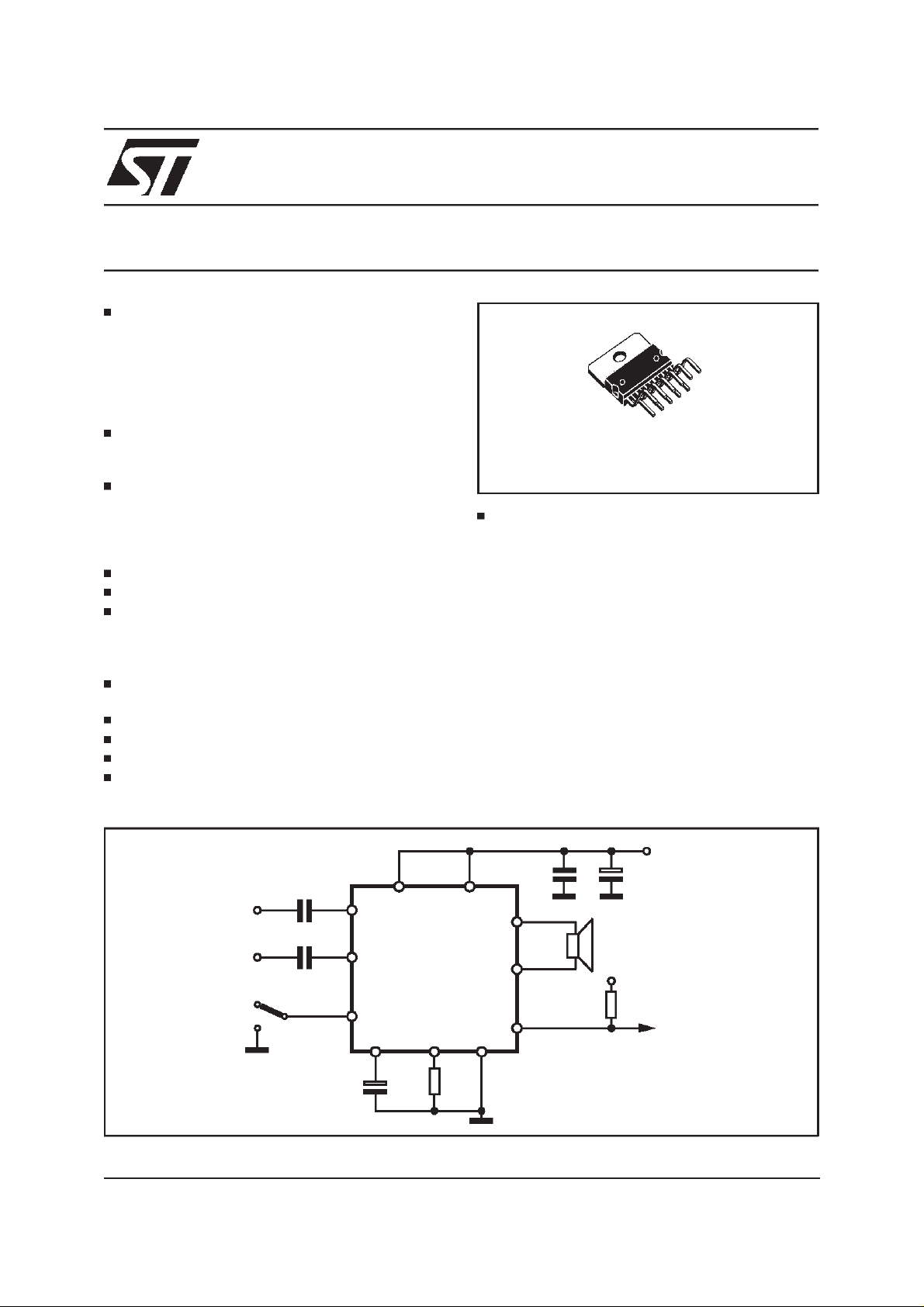
The TDA7391 is a BRIDGEclass AB audio power
amplifier specially intended for car radio High
Powerapplications.
The high power capabilitytogether withthe possibility to operate either in DIFFERENTIAL INPUT
MODE or SINGLEENDED INPUT MODE makes
it suitable for boosters and high end car radio
equipments.
The exclusive fully complementary output stage
and the internal fixed gain configuration drop the
externalcomponentcount.
The on board clipping detectorallowseasy implementationof gain compressionsystems.
Figure 1: Test AndApplication Circuit
+V
S
C4 1000µF
Vref
R1
4.7KΩ
TO µC
D94AU133
R2
56KΩ
C5 100nF
OUT+
7
OUT-
5
CD
4
GND
C2 0.22µF
39
C3
33µF
2
1
8
11
TDA7391
10 6
IN+
C1 0.22µF
IN-
V
S
SW1
October 1998
This is advanced informationon a new product now in development or undergoing evaluation. Details are subject to changewithout notice.
ST-BY
1/8
TDA7391
Figure 2: BlockDiagram
+
-
STANDBYTHRESHOLD
1
IN-
2
IN+
V
CC1VCC2
39
ICM
gm
+
COMMON
MODE
REFERENCES
-
+
V
CC/2
POWER AMP
LTS V=f (Tj)
POWER AMP
THD
DETECT
SHORT
DUMP &
PROTECTION
V
S
CIRCUIT
THERMAL
L
DISABLE
TS
5
OUT-
4
CD
7
OUT+
+
-
MUTE THRESHOLD
MUTE SYNC GND STANDBY
PIN CONNECTION(Topview)
TAB CONNECTED TO PIN 6
PROGRAMMABLE
CURRENT CIRCUIT
1011 8
6
D94AU134
11
10
9
8
7
6
5
4
3
2
1
D94AU135
MUTE
SYNC
+V
S
STAND-BY
OUT+
GND
OUTCD
+V
S
IN+
IN-
THERMAL DATA
Symbol Description Value Unit
Thermal Resistance Junction-case Max 1.8
2/8
R
th j-case
C/W
°
TDA7391
ABSOLUTE MAXIMUM RATINGS
Symbol Parameter Value Unit
V
V
V
PEAK
P
T
stg,Tj
OP
I
O
tot
DC Supply Voltage 28 V
S
Operating Supply Voltage 18 V
Peak Supply Voltage (t= 50ms) 50 V
Output Peak Current repetitive(f > 10Hz)
Output Peak Current non repetitive
Power Dissipation (T
=85°C) 43 W
CASE
4.5
6
Storage and Junction-Case Temperature -40 to 150
A
A
C
°
ELECTRICAL CHARACTERISTICS (VS= 14.4V; RL=4Ω, f = 1KHz, T
=25°C, unless otherwise
amb
specified)
Symbol Parameter Test Condition Min. Typ. Max. Unit
V
S
I
q
V
OS
I
SB
I
SBin
V
SBon
V
SBoff
ATT
ST-BY
I
Min
A
M
P
O
P
O EIAJ
P
O MAX
d Distortion
G
V
f
H
R
IN
E
IN
CMRR Input Common Mode Rejection f = 1KHz; V
SVR Supply Voltage Rejection R
CDL Clipping Detection Level 5 10 15 %
T
sd
(*) Saturated sqare wave output.
Supply Voltage Range 8 18 V
Total Quiescent Current 60 150 mA
Output Offset Voltage 120 mV
ST-BY Current V
ST-BY Input Bias Current V
= 1.5V 100
ST-BY
=5V 10
ST-BY
ST-BY On ThresholdVoltage 1.5 V
ST-BY Off thresholdVoltage 3.5 V
ST-BY Attenuation 90 dB
Mute Input BiasCurrent (V
= 5V) 10
MUTE
Mute Attenuation 90 dB
Output Power d = 10%
d=1%
d = 10%;R
= 3.2Ω
L
EIAJ Output Power (*) VS = 13.7V;RL= 3.2
MAX Output Power (*) VS= 14.4V; RL= 3.2
Ω
Ω
20 26
21
32
40 W
45 W
0.06
P
= 0.1 to 15W
O
0.03
Voltage Gain 29.5 30 30.5 dB
High Frequency rolloff PO= 1W; -3dB 75 KHz
Input Impedance Differential 36 60 KΩ
Single Ended 30 55 K
Input Noise Voltage Rg=0Ω;f= 22Hz to 22KHz 4 mV
= 1Vrms 65 dB
IN
=0Ω;Vr= 1Vrms 60 dB
g
Absolute Thermal Shutdown
160
Junction Temperature
A
µ
A
µ
A
µ
W
W
W
%
%
Ω
C
°
3/8
 Loading...