

ST TDA7389A User Manual
4 x 45W quad bridge car radio amplifier
Features
■ High output power:
– 4 x 45 W / 4 Ω max.
– 4 x 28 W / 4 Ω @ 14.4 V, 1 kHz, 10 %
■ Low distortion
■ Low output noise
■ Standby function
■ Mute function
■ Automute at min. supply voltage detection
■ Low external component count:
– Internally fixed gain (26dB)
– No external compensation
– No bootstrap capacitors
■ Clipping detector
■ Offset detector
■ Diagnostic facility for:
– Out to GND short
– Out to V
– Thermal shutdown
short
S
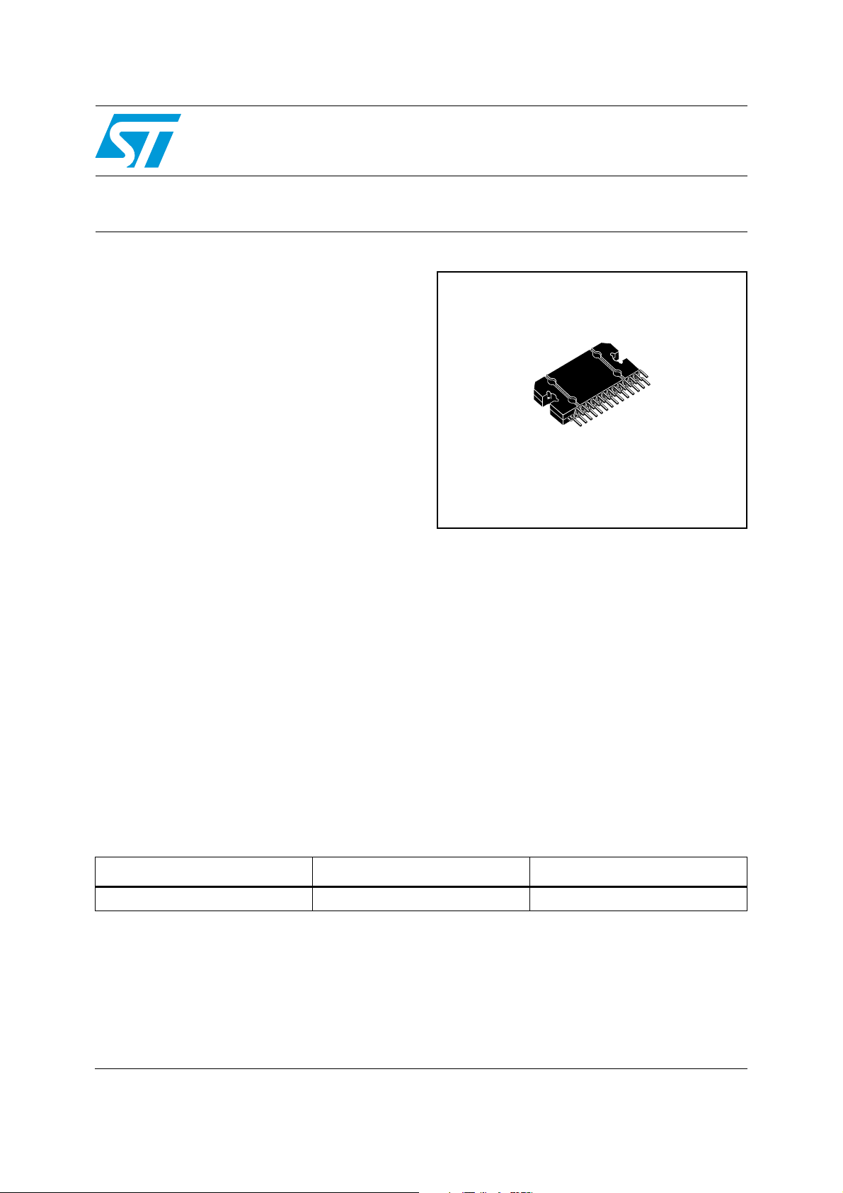
TDA7389A
Flexiwatt27
■ Load dump voltage
■ Fortuitous open GND
■ Output DC offset detector
■ Reversed battery
■ ESD
Description
Protections:
■ Output short circuit to GND, to V
load
■ Very inductive loads
■ Overrating chip temperature with soft thermal
limiter
Table 1. Device summary
Order code Package Packing
TDA7389A Flexiwatt27 Tube
October 2008 Rev 2 1/14
, across the
S
The TDA7389A is an AB class audio power
amplifier, packaged in Flexiwatt 27 designed for
high end car radio applications.
Based on the fully complementary PNP/NPN
configuration the TDA7389A allows a rail to rail
output voltage swing with no need of bootstrap
capacitors.
www.st.com
1

Contents TDA7389A
Contents
1 Pin connection and block diagrams . . . . . . . . . . . . . . . . . . . . . . . . . . . . 5
2 Electrical specifications . . . . . . . . . . . . . . . . . . . . . . . . . . . . . . . . . . . . . . 6
2.1 Absolute maximum ratings . . . . . . . . . . . . . . . . . . . . . . . . . . . . . . . . . . . . . 6
2.2 Thermal data . . . . . . . . . . . . . . . . . . . . . . . . . . . . . . . . . . . . . . . . . . . . . . . 6
2.3 Electrical characteristics . . . . . . . . . . . . . . . . . . . . . . . . . . . . . . . . . . . . . . . 6
2.4 Electrical characteristic curves . . . . . . . . . . . . . . . . . . . . . . . . . . . . . . . . . . 8
2.5 Test and application circuit . . . . . . . . . . . . . . . . . . . . . . . . . . . . . . . . . . . . 10
3 Application hints . . . . . . . . . . . . . . . . . . . . . . . . . . . . . . . . . . . . . . . . . . . 11
3.1 SVR . . . . . . . . . . . . . . . . . . . . . . . . . . . . . . . . . . . . . . . . . . . . . . . . . . . . . 11
3.2 Input stage . . . . . . . . . . . . . . . . . . . . . . . . . . . . . . . . . . . . . . . . . . . . . . . . 11
3.3 Standby and muting . . . . . . . . . . . . . . . . . . . . . . . . . . . . . . . . . . . . . . . . . 11
4 Package information . . . . . . . . . . . . . . . . . . . . . . . . . . . . . . . . . . . . . . . . 12
5 Revision history . . . . . . . . . . . . . . . . . . . . . . . . . . . . . . . . . . . . . . . . . . . 13
2/14

TDA7389A List of tables
List of tables
Table 1. Device summary . . . . . . . . . . . . . . . . . . . . . . . . . . . . . . . . . . . . . . . . . . . . . . . . . . . . . . . . . . 1
Table 2. Absolute maximum ratings . . . . . . . . . . . . . . . . . . . . . . . . . . . . . . . . . . . . . . . . . . . . . . . . . . 6
Table 3. Thermal data. . . . . . . . . . . . . . . . . . . . . . . . . . . . . . . . . . . . . . . . . . . . . . . . . . . . . . . . . . . . . 6
Table 4. Electrical characteristics . . . . . . . . . . . . . . . . . . . . . . . . . . . . . . . . . . . . . . . . . . . . . . . . . . . . 6
Table 5. Document revision history . . . . . . . . . . . . . . . . . . . . . . . . . . . . . . . . . . . . . . . . . . . . . . . . . 13
3/14

List of figures TDA7389A
List of figures
Figure 1. Block diagram . . . . . . . . . . . . . . . . . . . . . . . . . . . . . . . . . . . . . . . . . . . . . . . . . . . . . . . . . . . . 5
Figure 2. Pin connection (top view) . . . . . . . . . . . . . . . . . . . . . . . . . . . . . . . . . . . . . . . . . . . . . . . . . . . 5
Figure 3. Quiescent current vs. supply voltage . . . . . . . . . . . . . . . . . . . . . . . . . . . . . . . . . . . . . . . . . . 8
Figure 4. Quiescent output voltage vs. supply voltage . . . . . . . . . . . . . . . . . . . . . . . . . . . . . . . . . . . . 8
Figure 5. Output power vs. supply voltage . . . . . . . . . . . . . . . . . . . . . . . . . . . . . . . . . . . . . . . . . . . . . . 8
Figure 6. Maximum output power vs. supply voltage . . . . . . . . . . . . . . . . . . . . . . . . . . . . . . . . . . . . . . 8
Figure 7. Distortion vs. output power . . . . . . . . . . . . . . . . . . . . . . . . . . . . . . . . . . . . . . . . . . . . . . . . . . 8
Figure 8. Distortion vs. frequency . . . . . . . . . . . . . . . . . . . . . . . . . . . . . . . . . . . . . . . . . . . . . . . . . . . . 8
Figure 9. Supply voltage rejection vs. frequency . . . . . . . . . . . . . . . . . . . . . . . . . . . . . . . . . . . . . . . . . 9
Figure 10. Crosstalk vs. frequency . . . . . . . . . . . . . . . . . . . . . . . . . . . . . . . . . . . . . . . . . . . . . . . . . . . . 9
Figure 11. Output noise vs. source resistance. . . . . . . . . . . . . . . . . . . . . . . . . . . . . . . . . . . . . . . . . . . . 9
Figure 12. Power dissipation and efficiency vs. output power . . . . . . . . . . . . . . . . . . . . . . . . . . . . . . . . 9
Figure 13. ITU R-ARM frequency response, weighting filter for transient pop. . . . . . . . . . . . . . . . . . . . 9
Figure 14. Test and application circuit . . . . . . . . . . . . . . . . . . . . . . . . . . . . . . . . . . . . . . . . . . . . . . . . . 10
Figure 15. Flexiwatt27 mechanical data and package dimensions . . . . . . . . . . . . . . . . . . . . . . . . . . . 12
4/14
TDA7389A Pin connection and block diagrams
1 Pin connection and block diagrams
Figure 1. Block diagram
Vcc1 Vcc2
ST-BY
CD
OUT1+
OUT1-
PW-GND
OUT2+
OUT2-
PW-GND
OUT3+
OUT3-
PW-GND
OUT4+
OUT4-
PW-GND
D05AU1613
IN1
IN2
IN3
IN4
MUTE
AC-GND SVR TAB S-GND
OFFSET
DETECTOR
Figure 2. Pin connection (top view)
1
TAB
P-GND2
OFF.DET
OUT2-
ST-BY
CC
V
OUT2+
OUT1-
P-GND1
SVR
OUT1+
IN1
IN2
IN4
S-GND
IN3
OUT3+
AC-GND
OUT3-
P-GND3
CC
V
MUTE
OUT4+
FLEX27_O
OUT4-
P-GND4
CD
27
TAB
5/14
 Loading...