

ST TDA7386 User Manual
4 x 45 W quad bridge car radio amplifier
Features
■ High output power capability:
■ 4 x 45W/4Ω max.
■ 4 x 28W/4Ω @ 14.4V, 1KHz, 10%
■ 4 x 24W/4Ω @ 13.2V, 1KHz, 10%
■ Low distortion
■ Low output noise
■ Standby function
■ Mute function
■ Automute at min. supply voltage detection
■ Low external component count:
– Internally fixed gain (26dB)
– No external compensation
– No bootstrap capacitors
Protections
■ Output short circuit to GND, to V
load
■ Very inductive loads
■ Overrating chip temperature with soft thermal
limiter
Table 1. Device summary
, across the
S
TDA7386
Flexiwatt25
■ Load dump voltage
■ Fortuitous open GND
■ Reversed battery
■ ESD
Description
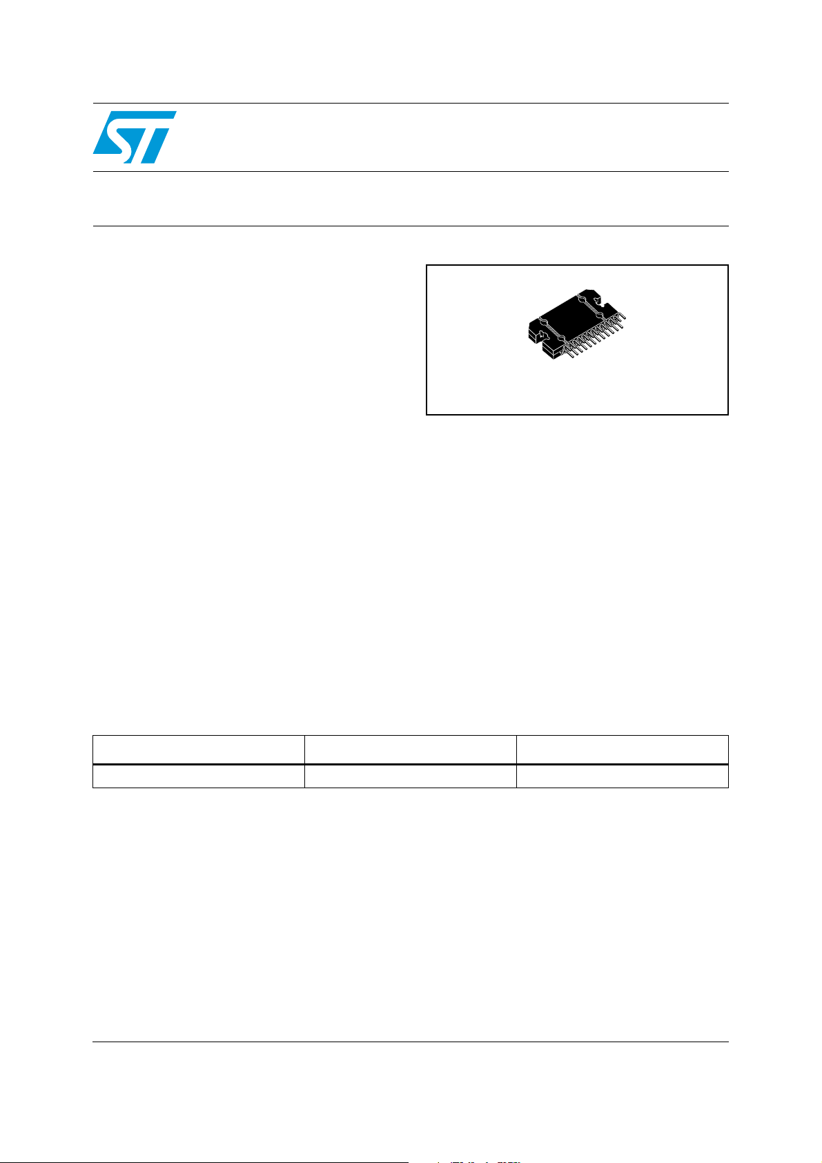
The TDA7386 is an AB class audio power
amplifier, packaged in Flexiwatt 25 and designed
for high end car radio applications.
Based on a fully complementary PNP/NPN
configuration, the TDA7386 allows a rail to rail
output voltage swing with no need of bootstrap
capacitors. The extremely reduced boundary
components count allows very compact sets.
Order code Package Packing
TDA7386 Flexiwatt25 Tube
November 2008 Rev 4 1/14
www.st.com
1

Contents TDA7386
Contents
1 Block and pin connection diagrams . . . . . . . . . . . . . . . . . . . . . . . . . . . . 5
2 Electrical specifications . . . . . . . . . . . . . . . . . . . . . . . . . . . . . . . . . . . . . . 6
2.1 Absolute maximum ratings . . . . . . . . . . . . . . . . . . . . . . . . . . . . . . . . . . . . . 6
2.2 Thermal data . . . . . . . . . . . . . . . . . . . . . . . . . . . . . . . . . . . . . . . . . . . . . . . 6
2.3 Electrical characteristics . . . . . . . . . . . . . . . . . . . . . . . . . . . . . . . . . . . . . . . 6
2.4 PCB and component layout . . . . . . . . . . . . . . . . . . . . . . . . . . . . . . . . . . . . 8
2.5 Electrical characteristics curves . . . . . . . . . . . . . . . . . . . . . . . . . . . . . . . . . 9
3 Application hints . . . . . . . . . . . . . . . . . . . . . . . . . . . . . . . . . . . . . . . . . . . 11
3.1 SVR . . . . . . . . . . . . . . . . . . . . . . . . . . . . . . . . . . . . . . . . . . . . . . . . . . . . . 11
3.2 Input stage . . . . . . . . . . . . . . . . . . . . . . . . . . . . . . . . . . . . . . . . . . . . . . . . 11
3.3 Standby and muting . . . . . . . . . . . . . . . . . . . . . . . . . . . . . . . . . . . . . . . . . 11
4 Package information . . . . . . . . . . . . . . . . . . . . . . . . . . . . . . . . . . . . . . . . 12
5 Revision history . . . . . . . . . . . . . . . . . . . . . . . . . . . . . . . . . . . . . . . . . . . 13
2/14

TDA7386 List of tables
List of tables
Table 1. Device summary . . . . . . . . . . . . . . . . . . . . . . . . . . . . . . . . . . . . . . . . . . . . . . . . . . . . . . . . . . 1
Table 2. Absolute maximum ratings . . . . . . . . . . . . . . . . . . . . . . . . . . . . . . . . . . . . . . . . . . . . . . . . . . 6
Table 3. Thermal data. . . . . . . . . . . . . . . . . . . . . . . . . . . . . . . . . . . . . . . . . . . . . . . . . . . . . . . . . . . . . 6
Table 4. Electrical characteristics . . . . . . . . . . . . . . . . . . . . . . . . . . . . . . . . . . . . . . . . . . . . . . . . . . . . 6
Table 5. Document revision history . . . . . . . . . . . . . . . . . . . . . . . . . . . . . . . . . . . . . . . . . . . . . . . . . 13
3/14

List of figures TDA7386
List of figures
Figure 1. Block diagram . . . . . . . . . . . . . . . . . . . . . . . . . . . . . . . . . . . . . . . . . . . . . . . . . . . . . . . . . . . . 5
Figure 2. Pin connection (top view) . . . . . . . . . . . . . . . . . . . . . . . . . . . . . . . . . . . . . . . . . . . . . . . . . . . 5
Figure 3. Standard test and application circuit. . . . . . . . . . . . . . . . . . . . . . . . . . . . . . . . . . . . . . . . . . . 7
Figure 4. Components and top copper layer . . . . . . . . . . . . . . . . . . . . . . . . . . . . . . . . . . . . . . . . . . . . 8
Figure 5. Bottom copper layer . . . . . . . . . . . . . . . . . . . . . . . . . . . . . . . . . . . . . . . . . . . . . . . . . . . . . . . 8
Figure 6. Quiescent current vs. supply voltage . . . . . . . . . . . . . . . . . . . . . . . . . . . . . . . . . . . . . . . . . . 9
Figure 7. Quiescent output voltage vs. supply voltage . . . . . . . . . . . . . . . . . . . . . . . . . . . . . . . . . . . . 9
Figure 8. Output power vs. supply voltage . . . . . . . . . . . . . . . . . . . . . . . . . . . . . . . . . . . . . . . . . . . . . . 9
Figure 9. Max. output power vs. supply voltage. . . . . . . . . . . . . . . . . . . . . . . . . . . . . . . . . . . . . . . . . . 9
Figure 10. Distortion vs. output power . . . . . . . . . . . . . . . . . . . . . . . . . . . . . . . . . . . . . . . . . . . . . . . . . . 9
Figure 11. Distortion vs. frequency . . . . . . . . . . . . . . . . . . . . . . . . . . . . . . . . . . . . . . . . . . . . . . . . . . . . 9
Figure 12. Supply voltage rejection vs. frequency . . . . . . . . . . . . . . . . . . . . . . . . . . . . . . . . . . . . . . . . 10
Figure 13. Crosstalk vs. frequency . . . . . . . . . . . . . . . . . . . . . . . . . . . . . . . . . . . . . . . . . . . . . . . . . . . 10
Figure 14. Output noise vs. source resistance. . . . . . . . . . . . . . . . . . . . . . . . . . . . . . . . . . . . . . . . . . . 10
Figure 15. Power dissipation and efficiency vs. output power . . . . . . . . . . . . . . . . . . . . . . . . . . . . . . . 10
Figure 16. Flexiwatt25 mechanical data and package dimensions . . . . . . . . . . . . . . . . . . . . . . . . . . . 12
4/14
TDA7386 Block and pin connection diagrams
1 Block and pin connection diagrams
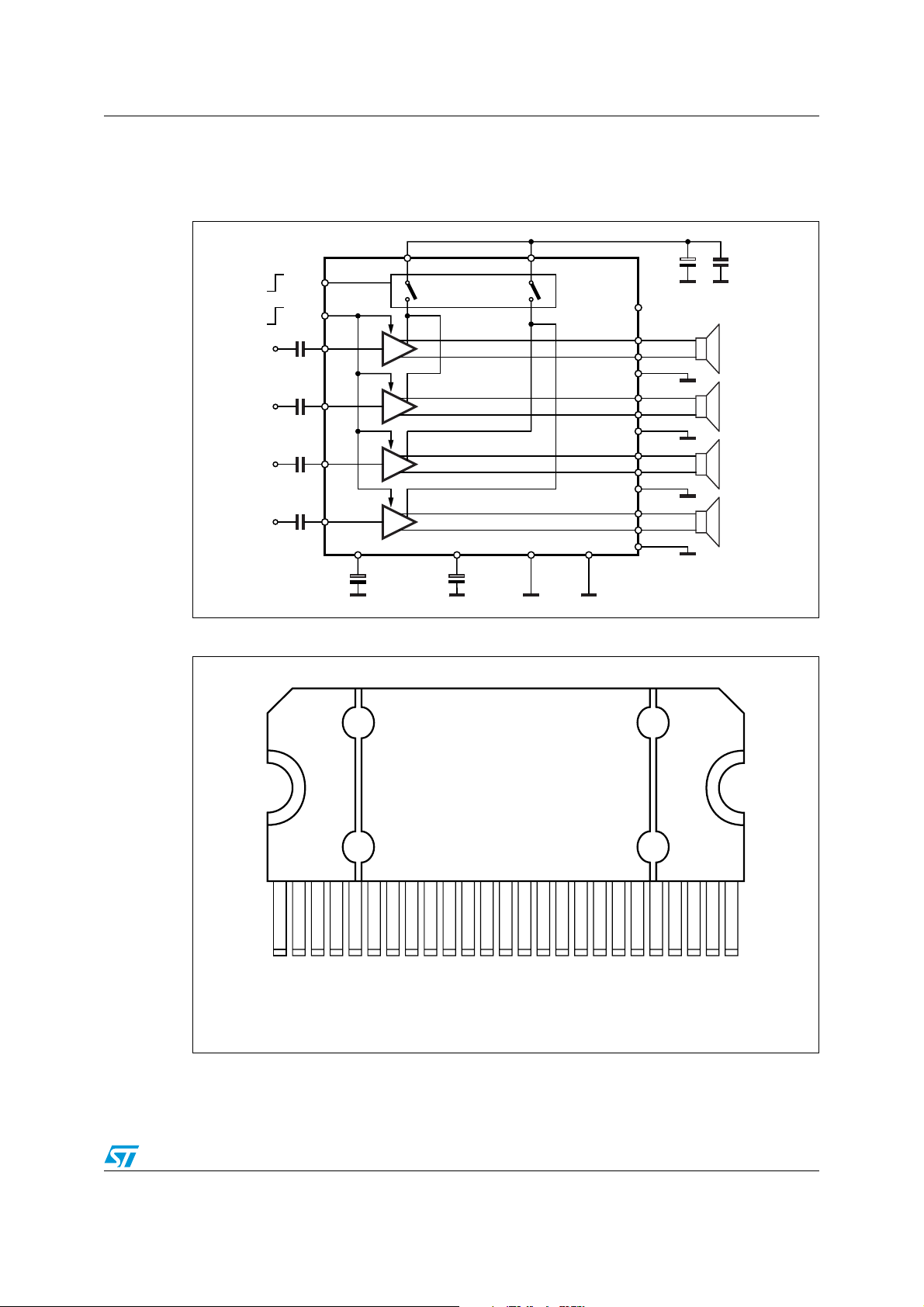
Figure 1. Block diagram
Vcc1 Vcc2
ST-BY
MUTE
IN1
0.1µF
IN2
0.1µF
IN3
0.1µF
IN4
0.1µF
AC-GND
0.47µF 47µF
SVR TAB S-GND
Figure 2. Pin connection (top view)
100nF2200µF
N.C.
OUT1+
OUT1-
PW-GND
OUT2+
OUT2-
PW-GND
OUT3+
OUT3-
PW-GND
OUT4+
OUT4-
PW-GND
D99AU1018A
1 25
TAB
OUT2-
P-GND2
ST-BY
OUT2+
V
CC
OUT1-
P-GND1
SVR
OUT1+
IN1
IN2
IN4
S-GND
IN3
OUT3+
AC-GND
OUT3-
P-GND3
CC
V
MUTE
OUT4+
D94AU159B
OUT4-
P-GND4
5/14
N.C.
 Loading...