

2 x 35 W power amplifier for car radio
Features
■ High output power capability:
– 2 x 40 W max./4 Ω
–2 x 35 W/4 Ω EIAJ
–2 x 25 W/4 Ω @14.4 V, 1 kHz, 10 %
–2 x 25 W/2 Ω @14.4 V, 1 kHz, 10 %
■ 2 Ω driving
■ Differential inputs
■ Minimum external components count
■ Internally fixed gain (26 dB)
■ Mute function (CMOS compatible)
■ Automute at minimum supply voltage detection
■ Standby function
■ No audible pop during mute and standby
operations
■ Clipping detector with programmable distortion
threshold
■ Protections:
– Short circuit (out to ground, out to supply
voltage, across the load)
– Overrating chip temperature with soft
thermal limiter
– Load dump voltage
– Fortuitous open ground
– Loudspeaker DC current
–ESD
Table 1. Device summary
TDA7376PD
PowerSO36 (Slug up)
Description
The TDA7376PD is a new technology dual bridge
audio amplifier in PowerSO36 package designed
for car radio applications.
Thanks to the fully complementary PNP/NPN
output stage configuration the TDA7376PD
delivers a rail-to-rail voltage swing with no need of
bootstrap capacitors.
Differential input pairs, that will accept either
single ended or differential input signals,
guarantee high noise immunity making the device
suitable for both car radio and car boosters
applications.
The audio mute control, that attenuates the output
signal of the audio amplifiers, suppresses pop
on - off transients and cuts any noises coming
from previous stages. The standby control, that
de-biases the amplifiers, reduces the cost of the
power switch. The on-board programmable
distortion detector allows compression facility
whenever the amplifier is overdriven, so limiting
the distortion at any levels inside the presettable
range.
Order code Package Packing
TDA7376PD PowerSO36 Tube
TDA7376PDTR PowerSO36 Tape and reel
December 2009 Doc ID 10260 Rev 3 1/14
www.st.com
1

Contents TDA7376PD
Contents
1 Block and pins connection diagrams . . . . . . . . . . . . . . . . . . . . . . . . . . . 5
2 Electrical specifications . . . . . . . . . . . . . . . . . . . . . . . . . . . . . . . . . . . . . . 6
2.1 Absolute maximum ratings . . . . . . . . . . . . . . . . . . . . . . . . . . . . . . . . . . . . . 6
2.2 Thermal data . . . . . . . . . . . . . . . . . . . . . . . . . . . . . . . . . . . . . . . . . . . . . . . 6
2.3 Electrical characteristics . . . . . . . . . . . . . . . . . . . . . . . . . . . . . . . . . . . . . . . 6
2.4 Electrical characteristics curves . . . . . . . . . . . . . . . . . . . . . . . . . . . . . . . . . 8
2.5 Test and application circuits . . . . . . . . . . . . . . . . . . . . . . . . . . . . . . . . . . . 10
3 Package information . . . . . . . . . . . . . . . . . . . . . . . . . . . . . . . . . . . . . . . . 12
4 Revision history . . . . . . . . . . . . . . . . . . . . . . . . . . . . . . . . . . . . . . . . . . . 13
2/14 Doc ID 10260 Rev 3

TDA7376PD List of tables
List of tables
Table 1. Device summary . . . . . . . . . . . . . . . . . . . . . . . . . . . . . . . . . . . . . . . . . . . . . . . . . . . . . . . . . . 1
Table 2. Absolute maximum ratings . . . . . . . . . . . . . . . . . . . . . . . . . . . . . . . . . . . . . . . . . . . . . . . . . . 6
Table 3. Thermal data. . . . . . . . . . . . . . . . . . . . . . . . . . . . . . . . . . . . . . . . . . . . . . . . . . . . . . . . . . . . . 6
Table 4. Electrical characteristics . . . . . . . . . . . . . . . . . . . . . . . . . . . . . . . . . . . . . . . . . . . . . . . . . . . . 6
Table 5. Document revision history . . . . . . . . . . . . . . . . . . . . . . . . . . . . . . . . . . . . . . . . . . . . . . . . . 13
Doc ID 10260 Rev 3 3/14

List of figures TDA7376PD
List of figures
Figure 1. Block diagram . . . . . . . . . . . . . . . . . . . . . . . . . . . . . . . . . . . . . . . . . . . . . . . . . . . . . . . . . . . . 5
Figure 2. Pins connection diagram (top view) . . . . . . . . . . . . . . . . . . . . . . . . . . . . . . . . . . . . . . . . . . . 5
Figure 3. Clip detector threshold vs. THD set. voltage . . . . . . . . . . . . . . . . . . . . . . . . . . . . . . . . . . . . 8
Figure 4. Quiescent current vs. supply voltage . . . . . . . . . . . . . . . . . . . . . . . . . . . . . . . . . . . . . . . . . . 8
Figure 5. Output power vs. supply voltage (THD = 1 %) . . . . . . . . . . . . . . . . . . . . . . . . . . . . . . . . . . . 8
Figure 6. Output power vs. supply voltage (THD = 10 %) . . . . . . . . . . . . . . . . . . . . . . . . . . . . . . . . . . 8
Figure 7. EIAJ power vs. supply voltage . . . . . . . . . . . . . . . . . . . . . . . . . . . . . . . . . . . . . . . . . . . . . . . 8
Figure 8. THD vs. frequency . . . . . . . . . . . . . . . . . . . . . . . . . . . . . . . . . . . . . . . . . . . . . . . . . . . . . . . . 8
Figure 9. THD vs. output power (RL = 4 W). . . . . . . . . . . . . . . . . . . . . . . . . . . . . . . . . . . . . . . . . . . . . 9
Figure 10. THD vs. output power (RL = 24 W). . . . . . . . . . . . . . . . . . . . . . . . . . . . . . . . . . . . . . . . . . . . 9
Figure 11. Dissipated power and efficiency vs. output power . . . . . . . . . . . . . . . . . . . . . . . . . . . . . . . . 9
Figure 12. SVR vs. frequency . . . . . . . . . . . . . . . . . . . . . . . . . . . . . . . . . . . . . . . . . . . . . . . . . . . . . . . . 9
Figure 13. CMRR vs. frequency. . . . . . . . . . . . . . . . . . . . . . . . . . . . . . . . . . . . . . . . . . . . . . . . . . . . . . . 9
Figure 14. Crosstalk vs. frequency . . . . . . . . . . . . . . . . . . . . . . . . . . . . . . . . . . . . . . . . . . . . . . . . . . . . 9
Figure 15. Differential inputs test and application circuit . . . . . . . . . . . . . . . . . . . . . . . . . . . . . . . . . . . 10
Figure 16. Single ended inputs test and application circuit . . . . . . . . . . . . . . . . . . . . . . . . . . . . . . . . . 10
Figure 17. Application board reference circuit . . . . . . . . . . . . . . . . . . . . . . . . . . . . . . . . . . . . . . . . . . . 11
Figure 18. PowerSO36 (slug up) mechanical data and package dimensions . . . . . . . . . . . . . . . . . . . 12
4/14 Doc ID 10260 Rev 3

TDA7376PD Block and pins connection diagrams
1 Block and pins connection diagrams
Figure 1. Block diagram
Figure 2. Pins connection diagram (top view)
NC
PWGND
PWGND
NC
OUT2+
OUT2+
NC
OUT2-
OUT2-
VCC
VCC
IN2+
IN2-
NC
NC
CD-OUT
THDSET
NC
36
35
34
33
32
31
30
29
28
26
25
23
22
21
20
19
D02AU1348
Doc ID 10260 Rev 3 5/14
1
2
3
4
5
6
7
8
9
1027
11
12
1324
14
15
16
17
18
TAB
TAB
PWGND
PWGND
NC
OUT1+
OUT1+
NC
OUT1-
OUT1-
VCC
VCC
IN1+
IN1-
NC
NC
MUTE
ST-BY
SGND

Electrical specifications TDA7376PD
2 Electrical specifications
2.1 Absolute maximum ratings
Table 2. Absolute maximum ratings
Symbol Parameter Value Unit
V
V
V
peak
Operating supply voltage 18 V
OP
DC supply voltage 28 V
s
Peak supply voltage (t = 50 ms) 50 V
Output peak current (not repetitive t = 100 μs) 8 A
I
O
Output peak current (repetitive f > 10 Hz) 6 A
P
T
stg
Power dissipation T
tot
, TjStorage and junction temperature -40 to 150 °C
= 85°C 36 W
case
2.2 Thermal data
Table 3. Thermal data
Symbol Parameter Value Unit
R
th j-case
Thermal resistance junction-to-case Max 2 °C/W
2.3 Electrical characteristics
Refer to the test circuits Figure 15 and 16, VS = 14.4 V; RL = 4 Ω; f = 1 kHz; T
unless otherwise specified.
Table 4. Electrical characteristics
= 25 °C,
amb
Symbol Parameter Test condition Min. Typ. Max. Unit
V
V
P
P
O max
P
O EIAJ
THD Distortion
C
Supply voltage range - 8 - 18 V
S
Total quiescent drain current RL = ∞ --200mA
I
d
Output offset voltage - - - 120 mV
OS
Output power
O
Max. output power
EIAJ output power
Cross talk
T
(1)
(1)
THD = 10 %;
THD = 10 %; R
= 2 Ω
L
23
33
-3640-W
VS = 13.7 V 32 35 - W
P
= 0.5 to 10 W
O
PO = 0.5 to 15 W
f = 1 kHz; R
f = 10 kHz; R
g
g
-
-
25
37
0.03
0.08
80
70
-W
-%
-dB
6/14 Doc ID 10260 Rev 3

TDA7376PD Electrical specifications
Table 4. Electrical characteristics (continued)
Symbol Parameter Test condition Min. Typ. Max. Unit
R
Input impedance
IN
differential input
Single Ended input
45
40
--kΩ
differential input 25 26 27 dB
G
ΔG
E
SVR Supply voltage rejection
Voltage gain
V
Channel gain balance - - - 1 dB
V
Input noise voltage
IN
Single Ended input 25 26 27 dB
R
= 600 Ω; "A" weighted
g
= 600 Ω; 22 Hz to 33 kHz
R
g
f = 100 Hz; V
f = 10 Hz; V
= 1 Vrms; Rg = 0;
r
= 1 Vrms; Rg = 0;
r
-
45
3
46
55
-dB
BW Power bandwidth (-3dB) 75 - - kHz
CMRR Common mode rejection ratio VCM = 1 Vrms input referred 60 - - dB
A
V
SB IN
V
SB OUT
I
A
V
M IN
V
M OUT
D
D
DOUT
1. Saturated square wave output
2. See Figure 3 for THD setting.
Standby attenuation VSB = 1.5V; P
SB
Standby input threshold - - - 1.5 V
Standby output threshold - 3.5 - - V
Standby current consumption VSB = 0V - - 20 μA
sb
Mute attenuation VM = 1.5 V; P
M
Mute in threshold - - - 1.5 V
Mute out threshold - 3.5 - - V
I
Mute pin current V6 = 0 to VS,; V
6
Distortion detection level
DL
Distortion detector output DC
current
(2)
-3.5--%
Output low, sinked current
(V
= 1.5 V)
pin10
Output high, leakage current
= VS, @ V
(V
pin10
= 1 W 80 90 dB
O ref
= 1 W - 85 - dB
Oref
= 18 V - - 100 μA
S max.
1--mA
Smax
= 18 V)
--10μA
μV
The TDA7376PD is equipped with a programmable clipping distortion detector circuitry that
allows to signal out the output stage saturation by providing a current sinking into an open
collector output (D
) when the total harmonic distortion of the output signal reaches the
DOUT
preset level. The desired threshold is fixed through an external divider that produces a
proper voltage level across the THD set pin. Figure 3 shows the THD detection threshold
versus the THD set voltage. Since it is essential that the THD set voltage be proportional to
the supply voltage, Figure 4 shows its value as a fraction of V
. The actual voltage can be
CC
computed by multiplying the fraction corresponding to the desired THD threshold by the
application’s supply voltage.
Doc ID 10260 Rev 3 7/14

Electrical specifications TDA7376PD
(V)
(V)
2.4 Electrical characteristics curves
VS = 14.4V
R
= 4
L
f = 1KHz
Po ( W)
f= 1 KHz
THD= 1 %
voltage
Ω
(THD = 1 %)
Vs
RL= 2
Ω
RL= 4
Figure 4. Quiescent current vs. supply volt-
age
RL = 4
Ω
Figure 6. Output power vs. supply voltage
(THD = 10 %)
Po ( W)
55
50
f= 1 KHz
45
THD= 10 %
40
35
30
25
Ω
20
15
10
5
8 9 10 11 12 13 14 15 16 17 18
RL= 2
Vs
Figure 3. Clip detector threshold vs. THD set.
Figure 5. Output power vs. supply voltage
45
40
35
30
25
20
15
10
5
8 9 10 11 12 13 14 15 16 17 18
Figure 7. EIAJ power vs. supply voltage Figure 8. THD vs. frequency
Ω
RL= 4
Ω
f = 1KHz
= 2.5Vrms
V
i
RL = 3.2
Ω
RL = 4
Ω
8/14 Doc ID 10260 Rev 3
VS = 14.4V
= 4
R
Ω
L
= 12W
P
O
f (Hz)

TDA7376PD Electrical specifications
Figure 9. THD vs. output power (RL = 4 Ω) Figure 10. THD vs. output power (RL = 24 Ω)
10
1
TH D (%)
Vs = 14.4 V
R L = 4
Ω
f= 10 KHz
10
1
THD (%)
Vs= 14.4 V
R L = 2
Ω
f = 10 KHz
0.1
f = 1 KHz
0.01
0.1 1 10
Po ( W)
Figure 11. Dissipated power and efficiency vs.
0.1
0.01
0.1 1 10
f= 1 KHz
Po ( W)
Figure 12. SVR vs. frequency
output power
VS = 14.4V
R
= 4
Ω
L
f = 1KHz
VS = 14.4V
= 4
R
Ω
L
= 1Vrms
V
r
Ri = 0
Ri = 600
f (Hz)
Ω
Ω
Figure 13. CMRR vs. frequency Figure 14. Crosstalk vs. frequency
VS = 14.4V
= 4
R
Ω
L
= 1Vrms
V
i
f (Hz)
Doc ID 10260 Rev 3 9/14
VS = 14.4V
= 4
R
Ω
L
= 1W
P
O
= 0
R
L
f (Hz)

Electrical specifications TDA7376PD
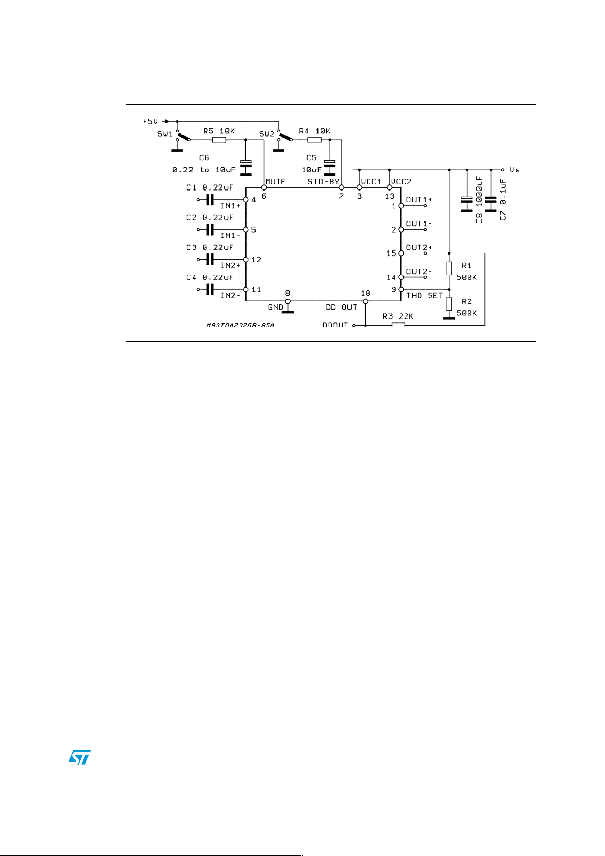
2.5 Test and application circuits
Figure 15. Differential inputs test and application circuit
Figure 16. Single ended inputs test and application circuit
10/14 Doc ID 10260 Rev 3
TDA7376PD Electrical specifications
Figure 17. Application board reference circuit
Doc ID 10260 Rev 3 11/14

Package information TDA7376PD
3 Package information
In order to meet environmental requirements, ST offers these devices in different grades of
ECOPACK
®
packages, depending on their level of environmental compliance. ECOPACK
®
specifications, grade definitions and product status are available at: www.st.com.
ECOPACK
®
is an ST trademark.
Figure 18. PowerSO36 (slug up) mechanical data and package dimensions
DIM.
A 3.270 - 3.410 0.1287 - 0.1343
A2 3.100 - 3.180 0.1220 - 0.1252
A4 0.800 - 1.000 0.0315 - 0.0394
A5 - 0.200 - - 0.0079 a1 0.030 -
b 0.220 - 0.380 0.0087 - 0.0150
c 0.230 - 0.320 0.0091 - 0.0126
D 15.800 - 16.000 0.6220 - 0.6299
D1 9.400 - 9.800 0.3701 - 0.3858
D2 - 1.000 - - 0.0394 -
E 13.900 - 14.500 0.5472 - 0.5709
E1 10.900 - 11.100 0.4291 - 0.4370
E2 - - 2.900 - - 0.1142
E3 5.800 - 6.200 0.2283 - 0.2441
E4 2.900 - 3.200 0.1142 - 0.1260
e - 0.650 - - 0.0256 e3 - 11.050 - - 0.4350 -
G 0 - 0.075 0 - 0.0031
H 15.500 - 15.900 0.6102 - 0.6260
h - - 1.100 - - 0.0433
L 0.800 - 1.100 0.0315 - 0.0433
N - - 10˚ - - 10˚
s - -8˚- -8˚
(1) “D and E1” do not include mold flash or protusions.
Mold flash or protusions shall not exceed 0.15mm (0.006”).
(2) No intrusion allowed inwards the leads.
mm inch
MIN. TYP. MAX. MIN. TYP. MAX.
-0.040
0.0012 - -0.0016
OUTLINE AND
MECHANICAL DATA
PowerSO36 (SLUG UP)
12/14 Doc ID 10260 Rev 3
7183931 G

TDA7376PD Revision history
4 Revision history
Table 5. Document revision history
Date Revision Changes
13-Dec-2003 1 Initial release.
16-Apr-2004 2 Corrected package drawing.
11-Dec-2009 3
Document reformatted.
Updated Section 3: Package information on page 12.
Doc ID 10260 Rev 3 13/14

TDA7376PD
Please Read Carefully:
Information in this document is provided solely in connection with ST products. STMicroelectronics NV and its subsidiaries (“ST”) reserve the
right to make changes, corrections, modifications or improvements, to this document, and the products and services described herein at any
time, without notice.
All ST products are sold pursuant to ST’s terms and conditions of sale.
Purchasers are solely responsible for the choice, selection and use of the ST products and services described herein, and ST assumes no
liability whatsoever relating to the choice, selection or use of the ST products and services described herein.
No license, express or implied, by estoppel or otherwise, to any intellectual property rights is granted under this document. If any part of this
document refers to any third party products or services it shall not be deemed a license grant by ST for the use of such third party products
or services, or any intellectual property contained therein or considered as a warranty covering the use in any manner whatsoever of such
third party products or services or any intellectual property contained therein.
UNLESS OTHERWISE SET FORTH IN ST’S TERMS AND CONDITIONS OF SALE ST DISCLAIMS ANY EXPRESS OR IMPLIED
WARRANTY WITH RESPECT TO THE USE AND/OR SALE OF ST PRODUCTS INCLUDING WITHOUT LIMITATION IMPLIED
WARRANTIES OF MERCHANTABILITY, FITNESS FOR A PARTICULAR PURPOSE (AND THEIR EQUIVALENTS UNDER THE LAWS
OF ANY JURISDICTION), OR INFRINGEMENT OF ANY PATENT, COPYRIGHT OR OTHER INTELLECTUAL PROPERTY RIGHT.
UNLESS EXPRESSLY APPROVED IN WRITING BY AN AUTHORIZED ST REPRESENTATIVE, ST PRODUCTS ARE NOT
RECOMMENDED, AUTHORIZED OR WARRANTED FOR USE IN MILITARY, AIR CRAFT, SPACE, LIFE SAVING, OR LIFE SUSTAINING
APPLICATIONS, NOR IN PRODUCTS OR SYSTEMS WHERE FAILURE OR MALFUNCTION MAY RESULT IN PERSONAL INJURY,
DEATH, OR SEVERE PROPERTY OR ENVIRONMENTAL DAMAGE. ST PRODUCTS WHICH ARE NOT SPECIFIED AS "AUTOMOTIVE
GRADE" MAY ONLY BE USED IN AUTOMOTIVE APPLICATIONS AT USER’S OWN RISK.
Resale of ST products with provisions different from the statements and/or technical features set forth in this document shall immediately void
any warranty granted by ST for the ST product or service described herein and shall not create or extend in any manner whatsoever, any
liability of ST.
ST and the ST logo are trademarks or registered trademarks of ST in various countries.
Information in this document supersedes and replaces all information previously supplied.
The ST logo is a registered trademark of STMicroelectronics. All other names are the property of their respective owners.
© 2009 STMicroelectronics - All rights reserved
STMicroelectronics group of companies
Australia - Belgium - Brazil - Canada - China - Czech Republic - Finland - France - Germany - Hong Kong - India - Israel - Italy - Japan -
Malaysia - Malta - Morocco - Philippines - Singapore - Spain - Sweden - Switzerland - United Kingdom - United States of America
www.st.com
14/14 Doc ID 10260 Rev 3
 Loading...