


®
4 x 6W POWER AMPLIFIER FOR CAR RADIO
HIGH POWER CAPABILITY:
4x6W min/4Ω @14.4V, 1KHz, 10%
4x10W typ/2Ω @14.4V, 1KHz, 10%
MINIMUM EXTERNAL COMPONEN T COUNT
- INTERNALLY FIXED GAIN (20dB)
- NO BOOTSTRAP CAPACITORS
- NO EXTERNAL COMPENSATION
ST-BY FUNCTION (CMOS COMPA TIBLE)
MUTE FUNCTION (CMOS COMPAT IBLE)
NO AUDIBLE POP DURING MUTE/ST-BY
OPERATIONS
LOW SUPPLY SELF MUTING
PROGRAMMABLE TURN ON DELAY
TDA7372A
MULTIWATT15
ORDERING NUMBER:
FORTUITOUS OPEN GND
REVERSED BATT ERY
ESD PROTECTION
TDA7372A
PROTECTIONS:
AC OUTPUT SHORT CIRCUIT TO GND
DC OUTPUT SHORT CIRCUIT TO GND AND
TO V
AT POWER ON
S
SOFT THERMAL LIMITER
OVERRATING CHIP TEMPERATURE
LOAD DUMP VOLTAGE
BLOCK DIAGRAM
DESCRIPTION
The TDA7372A is a new t echnolo gy c lass AB quad
channels Audio Power Amplifier in Multiwatt15
package designed for car radio applications.
Thanks to the fully complementary PNP/NPN output configuration the TDA7372A delivers a rail to
rail voltage swing with no need of boostrap capacitors.
September2003
This is advanced information on a new product now in development or undergoing evaluation. Details are subject to change without notice.
1/10
TDA7372A
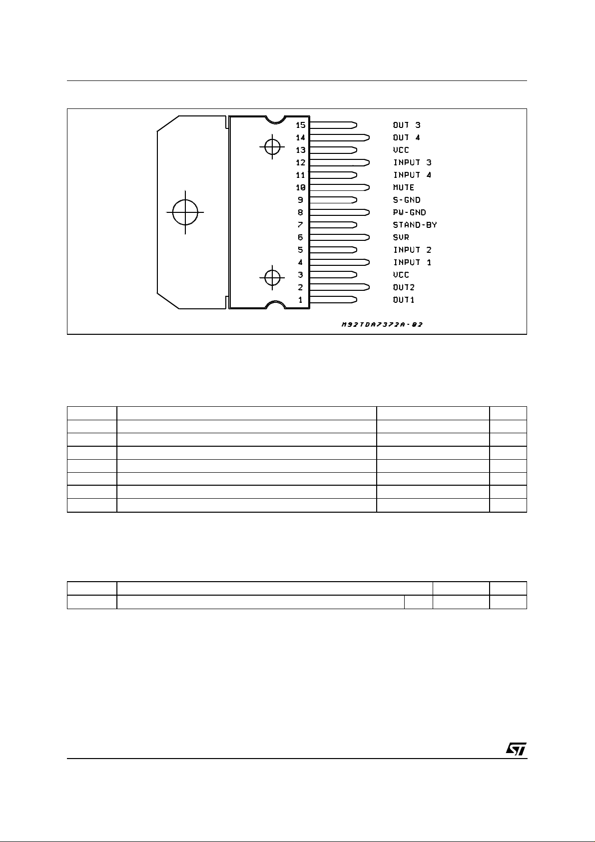
PIN CONNECTION
(Top view)
ABSOLUTE MAXIMUM RATINGS
Symbol Parameter Value Unit
DC Supply Voltage 28 V
S
Operating Supply Voltage 18 V
OP
Peak Supply Voltage (t = 50ms) 50 V
Output Peak Current (not rep. t = 100µs) 4 A
O
Output Peak Current (rep. f > 10Hz) 3 A
O
Power Dissipation (T
tot
= 85°C) 32 W
case
, TjStorage and Junction Temperature -40 to 150 °C
T
V
V
V
PEAK
I
I
P
stg
THERMAL DATA
Symbol Description Value Unit
R
th j-case
Thermal Resistance Junction-case Max 2 °C/W
2/10

TDA7372A
ELECTRICAL CHARACTERISTICS
(Refer to the test circuit; V
= 14.4V; RL = 4Ω, T
S
= 25°C,
amb
f = 1kHz, unless otherwise specified)
Symbol Parameter Test Condition Min. Typ. Max. Unit
V
S
I
d
P
O
d Distortion R
CT Cross Talk f = 1kHz; R
R
IN
G
V
G
V
BW Bandwidth @ -3dB 100 KHz
E
NO
SVR Supply Voltage Rejection R
ASB Stand-by Attenuation 80 dB
I
SB
I
PIN 7
V
SB IN
V
SB OUT
A
M
V
M IN
V
M OUT
(*) 22Hz to 22KHz
Supply Range 8 18 V
Total Quiescent Drain Current 150 mA
Output Power RL = 4Ω; THD = 10%
6 6.5 W
each channel
= 2Ω; THD = 10%
R
L
10 W
each channel
= 4Ω;
L
P
= 0.1 to 3W
O
f = 10kHz; R
g
= 0
= 0
g
54 60
0.04 0.3 %
55
Input Impedance 35 KΩ
Voltage Gain 19 20 21 dB
Voltage Gain Match. 1 dB
Output Noise Voltage (*) Rg = 0 120 µV
= 0; f = 100Hz 48 dB
g
ST-BY Current Consumption Vpin7 = 1.5V 100 µA
ST-BY Pin Current Play mode; Vpin7 = 5V 30 µA
Output Under Short (Max
5mA
driving current under fault)
ST-BY IN Threshold Voltage 1.5 V
ST-BY OUT Threshold Voltage 3.5 V
MUTE Attenuation 80 dB
MUTE IN Threshold Voltage 1.5 V
MUTE OUT Threshold Voltage 3.5 V
dB
dB
3/10

TDA7372A
TEST AND APPLICATION CIRCUIT
R2
10µF
C13
Figure 1:
P.C. Board and components layout of the Test and Application Circuit (1:1 scale)
4/10

TDA7372A
Figure 2:
Figure 4:
Quiescent Drain Current vs. Supply
Voltage
Output Power vs Supply Voltage
Figure 3:
Figure 5:
Output Power vs. Supply Voltage
Output power vs. Frequency vs.C
Value
OUT
Figure 6:
Distortion vs. Output Power
Figure 7:
Distortion vs. Output Power
5/10

TDA7372A
Figure 8:
Figure 10:
Distortion vs. Frequency
Cross-Talk vs. Frequency
Figure 9:
Figure 11:
Distortion vs. Frequency
Supply Voltage Rejection vs. Frequency
Figure 12:
P
(W)
tot
6/10
Total Power Dissipation and Efficiency
vs. Output Power
P
tot
Figure 13:
P
(W)
tot
Total Power Dissipation and Efficiency
vs. Output Power
P
tot

TDA7372A
Figure 14:
TDA7313 + 7372 Application Circuit
F
µ
10
7/10

TDA7372A
FUNCTIONAL DESCRIPTION
Function Description
The TDA7372A is a quad channel single package audio power amplifier intended to reduce the
GENERAL
OUTPUT STAGE
ST-BY
MUTE
THERMAL
PROTECTION
BUILT-IN SHORT
CIRCUIT
PROTECTION
mismatch in the electrical characteristics among the four different channels and to consistently
drop the external component count. It contains four non inverting stages capable to operate
down to 20dB gain so minimizing the output noise and optimizing SVR and distortion.
The output stage is a single ended type suitable to drive 4Ω loads. It consists of a class AB fully
complementary PNP/NPN stages short circuit protected.
A rail to rail output swing is achieved without need of boostrap capacitors. Moreover, the
external compensation is not necessary.
The device features a St-BY function which shuts down the internal bias generators when the
ST-BY input is low. In ST-BY mode the amplifier sinks a small current (in the range of few µAs).
When the St-BY pin is high the IC becomes fully operational.
A mute function is also provided. This reduces the gain of the input stage to a level effectively
eliminating any audio input influence on the output stage when the mute line is low. W hen the
mute line is high the normal input path is restored.
The device goes automatically into mute state when the supply voltage goes below the
minimum allowable value. This prevents pop noises whenever the battery voltage drops below
a fixed threshold. When the supply voltage rises to it nominal value the device recovers the play
condition with a delay fixed by the C
SVR
The Thermal protection principle involves two different steps
a) Soft thermal limitation
b) Shutdown
As long as the junction temperature remains below a preset threshold, the I.C. will deliver the
full power. Once the threshold has been reached, the device automatically goes into mute
status. The play to mute transition is internally controlled so producing a soft muting without
unpleasant effect. Supposing the junction temperature does not reduce to safe levels, a
complete shutdown will occur.
A built-in protection circuit assures reliable and safe operation in presence of:
- AC short circuit to GND
- DC short circuit to GND and to V
during power-on phase
S
The DC short protector acts in a way to avoid that the device is being turned on (by ST-BY)
when a DC short is present from OUT to GND or OUT to V
to introduce a proper delay on the st-by pin (expecially when it is driven by V
Moreover, as the involved circuitry is normally disabled when a current higher than 5mA is fed
into the st-by pin, it is important, in order not to disable it, to have the external current source
driving the pin itself limited to 5mA. (figure 1 is shows the relevant waveforms).
capacitor.
. Due to this reason it is necessary
S
.)
S
Figure 15:
8/10
Fault (DC short) waveforms

TDA7372A
DIM.
MIN. TYP. MAX. MIN. TYP. MAX.
A 5 0.197
B 2.65 0.104
C 1.6 0.063
D 1 0.039
E 0.49 0.55 0.019 0.022
F 0.66 0.75 0 .026 0 .030
G 1.02 1.27 1.52 0.040 0.050 0.060
G1 17.53 17.78 18.03 0.690 0.700 0.710
H1 19.6 0.772
H2 20.2 0.795
L 21.9 22.2 22.5 0.862 0.874 0.886
L1 21.7 22.1 2 2.5 0.854 0.870 0.886
L2 17.65 18.1 0 .695 0 .713
L3 17.25 17.5 17.75 0.679 0.689 0.699
L4 10.3 10.7 1 0.9 0.406 0.421 0.429
L7 2.65 2.9 0.104 0 .114
M 4.25 4.55 4.85 0.167 0.179 0.191
M1 4.63 5.08 5.53 0.182 0.200 0.218
S 1.9 2.6 0.075 0 .102
S1 1.9 2.6 0.075 0.102
Dia1 3.65 3.85 0 .144 0.152
mm inch
OUTLINE AND
MECHANICAL DATA
Multiwatt15 V
9/10

TDA7372A
Information furnishe d is beli eved to be accu rate and reliable. However, STMicroelec tronics assumes no res ponsibility for the consequences
of use of such i nformation nor for any i nfringement of patents or ot her rights of third par ties which may result from its use. No license i s
granted by imp lication or otherwi se under a ny patent or patent rights of STMicro electronics . Speci fications ment ioned in this publicat ion are
subject to change without notic e. This public ation supers edes and replaces all information prev iously supplied. STMic roelec tronic s products
are not authorized for use as critical components in life support devices or systems without express written approval of STMicroelectronics.
The ST logo is a registered trademark of STMicroelect roni cs.
All other names are the property of their respective owners
© 2003 STMicroelectronic s - All rights rese rved
STMicroelectronics GROUP OF COMPANIES
Australia – Belgium - Brazi l - Canada - China – Czec h Republ i c - Finland - France - Germany - Hong Kong - India - Israel - Italy - Japa n -
Malaysia - Malta - Morocco - Singapore - Spain - Sweden - Switzerland - United Kingdom - United States
www.st.com
10/10
 Loading...