

Page 1
Features
rd
■ 3
order high resolution sigma delta converter
for MPX sampling
■ Digital decimation and filtering stages
■ Demodulation of european radio data system
(RDS)
■ Demodulation of USA radio broadcast data
system (RBDS)
■ Automatic group and block synchronization
with flywheel mechanism
■ Error detection and correction
■ RAM buffer with a storage capacity of 24 RDS
blocks and related status information
■ Programmable interrupt source (RDS block A,
B, or D, TA, TA EON)
2
■ I
C/SPI bus interface
■ Input frequency range 4-21 MHz
■ Power down mode
■ 3.3 V power supply, 0.35 µm CMOS
technology
TDA7333N
RDS/RBDS processor
TSSOP16
Description
The TDA7333N circuit is a RDS/RDBS signal
processor, intended for recovering the inaudible
RDS/RBDS informations which are transmitted on
most FM radio broadcasting stations..
Table 1. Device summary
Order code Operating temp. range, °C Package Packing
TDA7333N -40 to +85 TSSOP16 Tube
TDA7333NTR -40 to +85 TSSOP16 Tape & reel
September 2009 Doc ID 12064 Rev 4 1/36
www.st.com
1
Page 2

Contents TDA7333N
Contents
1 Block diagram and pin description . . . . . . . . . . . . . . . . . . . . . . . . . . . . . 6
1.1 Block diagram . . . . . . . . . . . . . . . . . . . . . . . . . . . . . . . . . . . . . . . . . . . . . . . 6
1.2 Pin description . . . . . . . . . . . . . . . . . . . . . . . . . . . . . . . . . . . . . . . . . . . . . . 6
2 Electrical specifications . . . . . . . . . . . . . . . . . . . . . . . . . . . . . . . . . . . . . . 8
2.1 Absolute maximum ratings . . . . . . . . . . . . . . . . . . . . . . . . . . . . . . . . . . . . . 8
2.2 General interface electrical characteristics . . . . . . . . . . . . . . . . . . . . . . . . . 8
2.3 Electrical characteristics . . . . . . . . . . . . . . . . . . . . . . . . . . . . . . . . . . . . . . . 8
3 Functional description . . . . . . . . . . . . . . . . . . . . . . . . . . . . . . . . . . . . . . 11
3.1 Overview . . . . . . . . . . . . . . . . . . . . . . . . . . . . . . . . . . . . . . . . . . . . . . . . . 11
3.2 Fractional PLL . . . . . . . . . . . . . . . . . . . . . . . . . . . . . . . . . . . . . . . . . . . . . 11
3.3 Sigma delta converter . . . . . . . . . . . . . . . . . . . . . . . . . . . . . . . . . . . . . . . 12
3.4 Demodulator . . . . . . . . . . . . . . . . . . . . . . . . . . . . . . . . . . . . . . . . . . . . . . . 12
3.5 Group and block synchronization module . . . . . . . . . . . . . . . . . . . . . . . . 14
3.6 Flywheel mechanism . . . . . . . . . . . . . . . . . . . . . . . . . . . . . . . . . . . . . . . . 16
3.7 RAM Buffer . . . . . . . . . . . . . . . . . . . . . . . . . . . . . . . . . . . . . . . . . . . . . . . . 18
3.8 Programming through serial bus interface . . . . . . . . . . . . . . . . . . . . . . . . 20
3.8.1 rds_int register . . . . . . . . . . . . . . . . . . . . . . . . . . . . . . . . . . . . . . . . . . . . 21
3.8.2 rds_qu register . . . . . . . . . . . . . . . . . . . . . . . . . . . . . . . . . . . . . . . . . . . . 22
3.8.3 rds_corrp register . . . . . . . . . . . . . . . . . . . . . . . . . . . . . . . . . . . . . . . . . . 22
3.8.4 rds_bd_h register . . . . . . . . . . . . . . . . . . . . . . . . . . . . . . . . . . . . . . . . . . 23
3.8.5 rds_bd_l register . . . . . . . . . . . . . . . . . . . . . . . . . . . . . . . . . . . . . . . . . . 23
3.8.6 rds_bd_ctrl register . . . . . . . . . . . . . . . . . . . . . . . . . . . . . . . . . . . . . . . . 24
3.8.7 sinc4reg register . . . . . . . . . . . . . . . . . . . . . . . . . . . . . . . . . . . . . . . . . . 24
3.8.8 testreg register . . . . . . . . . . . . . . . . . . . . . . . . . . . . . . . . . . . . . . . . . . . . 24
3.8.9 pllreg4 register . . . . . . . . . . . . . . . . . . . . . . . . . . . . . . . . . . . . . . . . . . . . 25
3.8.10 pllreg3 register . . . . . . . . . . . . . . . . . . . . . . . . . . . . . . . . . . . . . . . . . . . . 25
3.8.11 pllreg2 register . . . . . . . . . . . . . . . . . . . . . . . . . . . . . . . . . . . . . . . . . . . . 26
3.8.12 pllreg1 register . . . . . . . . . . . . . . . . . . . . . . . . . . . . . . . . . . . . . . . . . . . . 26
3.8.13 pllreg0 register . . . . . . . . . . . . . . . . . . . . . . . . . . . . . . . . . . . . . . . . . . . . 26
3.9 I2C transfer mode . . . . . . . . . . . . . . . . . . . . . . . . . . . . . . . . . . . . . . . . . . . 27
3.9.1 Write transfer . . . . . . . . . . . . . . . . . . . . . . . . . . . . . . . . . . . . . . . . . . . . . 28
2/36 Doc ID 12064 Rev 4
Page 3

TDA7333N Contents
3.9.2 Read transfer . . . . . . . . . . . . . . . . . . . . . . . . . . . . . . . . . . . . . . . . . . . . . 28
3.10 SPI Mode . . . . . . . . . . . . . . . . . . . . . . . . . . . . . . . . . . . . . . . . . . . . . . . . . 30
4 Application notes . . . . . . . . . . . . . . . . . . . . . . . . . . . . . . . . . . . . . . . . . . 33
4.1 Typical RDS data transfer . . . . . . . . . . . . . . . . . . . . . . . . . . . . . . . . . . . . . 33
5 Package information . . . . . . . . . . . . . . . . . . . . . . . . . . . . . . . . . . . . . . . . 34
6 Revision history . . . . . . . . . . . . . . . . . . . . . . . . . . . . . . . . . . . . . . . . . . . 35
Doc ID 12064 Rev 4 3/36
Page 4

List of tables TDA7333N
List of tables
Table 1. Device summary . . . . . . . . . . . . . . . . . . . . . . . . . . . . . . . . . . . . . . . . . . . . . . . . . . . . . . . . . . 1
Table 2. Pin description . . . . . . . . . . . . . . . . . . . . . . . . . . . . . . . . . . . . . . . . . . . . . . . . . . . . . . . . . . . 7
Table 3. Absolute maximum ratings . . . . . . . . . . . . . . . . . . . . . . . . . . . . . . . . . . . . . . . . . . . . . . . . . . 8
Table 4. General interface electrical characteristics . . . . . . . . . . . . . . . . . . . . . . . . . . . . . . . . . . . . . . 8
Table 5. Electrical characteristics . . . . . . . . . . . . . . . . . . . . . . . . . . . . . . . . . . . . . . . . . . . . . . . . . . . . 8
Table 6. External pins alternate functions. . . . . . . . . . . . . . . . . . . . . . . . . . . . . . . . . . . . . . . . . . . . . 20
Table 7. Registers description . . . . . . . . . . . . . . . . . . . . . . . . . . . . . . . . . . . . . . . . . . . . . . . . . . . . . 20
Table 8. Document revision history . . . . . . . . . . . . . . . . . . . . . . . . . . . . . . . . . . . . . . . . . . . . . . . . . 35
4/36 Doc ID 12064 Rev 4
Page 5

TDA7333N List of figures
List of figures
Figure 1. Block diagram . . . . . . . . . . . . . . . . . . . . . . . . . . . . . . . . . . . . . . . . . . . . . . . . . . . . . . . . . . . . 6
Figure 2. Pin connection (top view) . . . . . . . . . . . . . . . . . . . . . . . . . . . . . . . . . . . . . . . . . . . . . . . . . . . 6
Figure 3. Fractional PLL. . . . . . . . . . . . . . . . . . . . . . . . . . . . . . . . . . . . . . . . . . . . . . . . . . . . . . . . . . . 11
Figure 4. Demodulator block diagram . . . . . . . . . . . . . . . . . . . . . . . . . . . . . . . . . . . . . . . . . . . . . . . . 13
Figure 5. Group and block synchronization diagram . . . . . . . . . . . . . . . . . . . . . . . . . . . . . . . . . . . . . 14
Figure 6. Example for flywheel mechanism . . . . . . . . . . . . . . . . . . . . . . . . . . . . . . . . . . . . . . . . . . . . 16
Figure 7. RAM buffer usage . . . . . . . . . . . . . . . . . . . . . . . . . . . . . . . . . . . . . . . . . . . . . . . . . . . . . . . . 18
Figure 8. RAM buffer update depends on “syncw” bit rds_bd_ctrl[0] . . . . . . . . . . . . . . . . . . . . . . . . . 18
Figure 9. RAM buffer states . . . . . . . . . . . . . . . . . . . . . . . . . . . . . . . . . . . . . . . . . . . . . . . . . . . . . . . . 19
Figure 10. rds_int registe . . . . . . . . . . . . . . . . . . . . . . . . . . . . . . . . . . . . . . . . . . . . . . . . . . . . . . . . . . . 21
Figure 11. rds_qu register . . . . . . . . . . . . . . . . . . . . . . . . . . . . . . . . . . . . . . . . . . . . . . . . . . . . . . . . . . 22
Figure 12. rds_corrp register . . . . . . . . . . . . . . . . . . . . . . . . . . . . . . . . . . . . . . . . . . . . . . . . . . . . . . . . 22
Figure 13. rds_bd_h registe . . . . . . . . . . . . . . . . . . . . . . . . . . . . . . . . . . . . . . . . . . . . . . . . . . . . . . . . . 23
Figure 14. rds_bd_l register . . . . . . . . . . . . . . . . . . . . . . . . . . . . . . . . . . . . . . . . . . . . . . . . . . . . . . . . . 23
Figure 15. rds_bd_ctrl register . . . . . . . . . . . . . . . . . . . . . . . . . . . . . . . . . . . . . . . . . . . . . . . . . . . . . . . 24
Figure 16. sinc4reg register . . . . . . . . . . . . . . . . . . . . . . . . . . . . . . . . . . . . . . . . . . . . . . . . . . . . . . . . . 24
Figure 17. testreg register . . . . . . . . . . . . . . . . . . . . . . . . . . . . . . . . . . . . . . . . . . . . . . . . . . . . . . . . . . 24
Figure 18. pllreg4 register . . . . . . . . . . . . . . . . . . . . . . . . . . . . . . . . . . . . . . . . . . . . . . . . . . . . . . . . . . 25
Figure 19. pllreg3 register . . . . . . . . . . . . . . . . . . . . . . . . . . . . . . . . . . . . . . . . . . . . . . . . . . . . . . . . . . 25
Figure 20. pllreg2 register . . . . . . . . . . . . . . . . . . . . . . . . . . . . . . . . . . . . . . . . . . . . . . . . . . . . . . . . . . 26
Figure 21. pllreg1 register . . . . . . . . . . . . . . . . . . . . . . . . . . . . . . . . . . . . . . . . . . . . . . . . . . . . . . . . . . 26
Figure 22. pllreg0 register . . . . . . . . . . . . . . . . . . . . . . . . . . . . . . . . . . . . . . . . . . . . . . . . . . . . . . . . . . 26
Figure 23. I
Figure 24. I
Figure 25. I
Figure 26. I
Figure 27. I
Figure 28. I
Figure 29. SPI data transfer . . . . . . . . . . . . . . . . . . . . . . . . . . . . . . . . . . . . . . . . . . . . . . . . . . . . . . . . . 30
Figure 30.
Figure 31. Read out RDS data and related flags, no update of rds_int and rds_bd_ctrl registers. . . . 31
Figure 32. Write rds_int registers in SPI mode, reading 1 register . . . . . . . . . . . . . . . . . . . . . . . . . . . 32
Figure 33. TSSOP16 mechanical data and package dimensions . . . . . . . . . . . . . . . . . . . . . . . . . . . . 34
2
C data transfer . . . . . . . . . . . . . . . . . . . . . . . . . . . . . . . . . . . . . . . . . . . . . . . . . . . . . . . . . 27
2
C write transfer . . . . . . . . . . . . . . . . . . . . . . . . . . . . . . . . . . . . . . . . . . . . . . . . . . . . . . . . . 28
2
C write operation example: write of rds_int and rds_bd_ctrl registers . . . . . . . . . . . . . . . 28
2
C read transfer . . . . . . . . . . . . . . . . . . . . . . . . . . . . . . . . . . . . . . . . . . . . . . . . . . . . . . . . . 28
2
C read access example 1: read of 5 bytes . . . . . . . . . . . . . . . . . . . . . . . . . . . . . . . . . . . . 29
2
C read access example 2: read of 1 byte. . . . . . . . . . . . . . . . . . . . . . . . . . . . . . . . . . . . . 30
Write rds_int, rds_bd_ctrl and pll_reg4 registers in SPI mode, reading RDS data and related flags
. 31
Doc ID 12064 Rev 4 5/36
Page 6
Block diagram and pin description TDA7333N
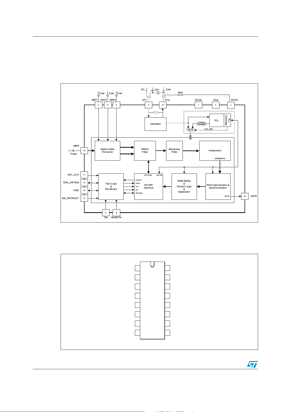
1 Block diagram and pin description
1.1 Block diagram
Figure 1. Block diagram
1.2 Pin description
Figure 2. Pin connection (top view)
VDDA
1
REF3
2
REF2
3
REF1
4
VSS
TM
RESETN
6/36 Doc ID 12064 Rev 4
TDA7333N
5
6
7
8
MPX
16
INTN
15
CSN
14
SA_DATAOUT
13
SDA_DATAIN
12
SCL_CLK
11
XTOVDDD
10
XTI
9
Page 7

TDA7333N Block diagram and pin description
Table 2. Pin description
Pin # Pin name Function
1 VDDA Analog supply voltage
2 REF3 Reference voltage 3 of A/D converter (2.65 V)
3 REF2 Reference voltage 2 of A/D converter (1.65 V)
4 REF1 Reference voltage 1 of A/D converter (0.65 V)
5 VSS Common ground
6TM
7 VDDD Digital supply voltage
8 RESETN External reset input (active low)
9 XTI Oscillator input
10 XTO Oscillator output
11 SCL_CLK Clock signal for I
12 SDA_DATAIN Data line in I
13 SA_DATAOUT Slave address in I
14 CSN Chip select (1 = I
15 INTN
Testmode selection (scan test).
Normal mode must be connected to gnd.
2
C and SPI modes
2
C mode, data input in SPI mode
2
C mode, data output in SPI mode
2
C mode, 0=SPI mode)
Interrupt output (active low), prog. at buff.not empty,buff. full, block A,B,D
,TA, TA EON
16 MPX Multiplex input signal
Doc ID 12064 Rev 4 7/36
Page 8

Electrical specifications TDA7333N
2 Electrical specifications
2.1 Absolute maximum ratings
Table 3. Absolute maximum ratings
Symbol Parameter Test conditions Min. Typ. Max. Unit
V
V
V
T
3.3 V power supply voltages - -0.5 - 4 V
DD
Input voltage 5 V tolerant inputs -0.5 - 5.5 V
in
Output voltage 5 V tolerant output buffers in tri-state -0.5 - 5.5 V
out
Storage temperature - -55 - 150 °C
stg
Human body model ≥ ±2000 V
V
ESD withstand voltage
ESD
Machine model ≥ ±200 V
Charged device model, corner pins ≥ ±1000 V
2.2 General interface electrical characteristics
Table 4. General interface electrical characteristics
Symbol Parameter Test conditions Min. Typ. Max. Unit
I
il
I
ih
I
ozFT
Low level input current Vi = 0 V - - 1 µA
High level input current Vi = V
Five volt tolerant tri-state
Vo = 0 V or V
DD
DD
--1µA
--1µA
output leakage without pull
= 5.5 V - 1 3 µA
V
up/down device
o
2.3 Electrical characteristics
T
= -40 to +85 °C, V
amb
V
and V
DDD
Table 5. Electrical characteristics
must not differ more than 0.15 V
DDA
DDA/VDDD
Symbol Parameter Test conditions Min. Typ. Max. Unit
Supply (pin 1,5,7)
V
V
I
I
DDD
DDA
DDD
DDA
Digital supply voltage - 3.0 3.3 3.6 V
Analog supply voltage - 3.0 3.3 3.6 V
Digital supply current
Analog supply current
8/36 Doc ID 12064 Rev 4
= 3.0 to 3.6 V, f
= 8.55 MHz, unless otherwise specified
osc
Normal mode - 14 - mA
Power down mode - < 1 - µA
Normal mode - 11.7 - mA
Power down mode - < 1 - mA
Page 9

TDA7333N Electrical specifications
Table 5. Electrical characteristics (continued)
Symbol Parameter Test conditions Min. Typ. Max. Unit
Digital inputs( pin 6,8,11,12,13,14)
Low level input voltage - - - 0.8 V
il
High level input voltage - 2.0 - - V
ih
Low level threshold input
falling
High level threshold input
rising
Schmitt trigger hysteresis - 0.4 - 0.7 V
hst
-1.0-1.15V
- 1.5 - 1.7 V
V
V
V
V
ilhyst
ihhyst
V
Digital outputs (pin 12,13,15) are open drains
V
V
High level output Voltage
oh
Low level output Voltage
ol
Open drain, depends on external
circuitry
I
=4 mA, takes into account
ol
200 mV drop in the supply voltage
-n/a-V
--0.4V
Analog inputs (pin 16)
V
MPX
Input Range of MPX Signal - - - 0.75 Vrms
- Input Impedance of MPX pin - - 55k - Ohm
C
Blocking Capac. of REF Pins
ref
Electrolyte capacitor parallel to
ceramic capacitor
-2.2-μF
-100-nF
Crystal/oscillator parameters
f
osc
f
oto
t
g
C
xti,Cxto
Quartz frequency - 4 10.25 21 MHz
Total quartz frequency
tolerance
Start up time - - - 10 ms
su
Oscillator transconductance - 0.0006 - - A/V
m
Load capacitance With crystal between XTI and XTO - 16 - pF
External XTI input frequency mode (pin 9)
f
exti
V
C
R
Externaly applied XTI
frequency
XTI input voltage
xti
Coupling capacitor for external
in
clock frequency
XTO pull up to VDDD - - 3.3 - kΩ
xto
T
= -40 to 85 °C - - 100 ppm
amb
- 4 10.25 21 MHz
With R
and f
= 3.3 kOhm,
xto
= 10.25 MHz
exti
220 - - mVpp
- - 100 - pF
Doc ID 12064 Rev 4 9/36
Page 10

Electrical specifications TDA7333N
Table 5. Electrical characteristics (continued)
Symbol Parameter Test conditions Min. Typ. Max. Unit
PLL parameters
f
t
O
vco
f
lock
I
M
VCO range - 150 - 250 MHz
VCO input range - 4 - 21 MHz
vin
PLL lock time - - - 500 µs
Input divide factor - 1 - 32 -
DF
Output divide factor - 2 - 32 -
DF
Integer multiplication factor - 10 - 128 -
F
FRA Fractional multiplication factor FRA/2
Bandpass filter
f
Pass-band frequencies - 55.6 - 58.4 kHz
p
R
f
stop
R
2
I
C (@ fsys = 8.55/8.664 MHz)
f
I2C
ts
Pass-band ripple - -0.5 - +0.5 dB
p
Stop-band corner frequencies - 53 - 61 kHz
Stop-band attenuation - - -43 - dB
s
Clock frequency in I2C mode - - - 400 kHz
Data setup time - 250 - - ns
udat
SPI (@ fsys = 8.55/8.664 MHz)
f
t
t
t
SPI
t
t
csu
csh
odv
t
t
Clock frequency in SPI mode - - - 1 MHz
Clock high time - 450 - - ns
ch
Clock low time - 450 - - ns
cl
Chip select setup time - 500 - - ns
Chip select hold - 500 - - ns
Output data valid - - - 250 ns
Output hold - 0 - - ns
oh
Deselect time - 1000 - - ns
t
d
Data setup time - 200 - - ns
su
Data hold time - 200 - - ns
t
h
14
0-214-
10/36 Doc ID 12064 Rev 4
Page 11
TDA7333N Functional description
3 Functional description
3.1 Overview
The new RDS/RBDS processor contains all RDS/RBDS relevant functions on a single chip.
It recovers the inaudible RDS/RBDS information which are transmitted on most FM radio
broadcasting stations.
The oscillator frequency can be derived from the tuner with typical value of 10.25 MHz . The
device can operate with frequencies in the range of 4-21 MHz. Therefor the fractional PLL
must be initialized through I
reference clock with a freq. tolerance of ±0.7 kHz.
Due to an integrated 3
further processing is done in the digital. After filtering the highly over sampled output of the
A/D converter, the RDS/RBDS demodulator extracts the RDS data clock, RDS data signal
and the quality information. A next RDS/RBDS decoder will synchronize the bit wise RDS
stream to a group and block wise information. This processing includes an error detection
and error correction algorithm. In addition, an automatic flywheel control avoids overheads
in the data exchange between the RDS/RBDS processor and the host.
The device operates in accordance with the CENELEC Radio Data System (RDS)
specification EN50067.
2
C/SPI interface to generate the internal 8.55 MHz or 8.664 MHz
rd
order sigma delta converter, which samples the MPX signal, all
3.2 Fractional PLL
Figure 3. Fractional PLL
XTI)
f(
) = 8.55/
PLL
8.664 MHz
f(
Input
Divider
IDF
Phase
Comperator
& VCO
Fractional
Divider
14
FRAEN
MF + FRA/2
PLL ControllerMux
DITEN
f(vco)
LOCK
Output
Divider
ODF
fsys
pllreg4
pllreg3
pllreg2
pllreg1
pllreg0
Doc ID 12064 Rev 4 11/36
Page 12

Functional description TDA7333N
The fractional PLL (Figure 3) is used to generate from the XTI input clock one of the two
possible system clocks (fsys) 8.55 MHz or 8.664 MHz. For this a setting for the input diver
factor (IDF), output divider factor (ODF), multiplication factor (MF) and fractional factor
(FRA) must be found (max. fsys tolerance ±0.7 kHz). For fractional mode an additional
dither can be enabled (DITEN) to eliminate tones in the PLL output clock. The fractional
mode can be disabled (FRAEN) if not needed.
The system clock (fsys) is equal to the XTI input clock after reset. After the PLL is locked,
the system clock will switch automatically to the PLL output clock. Then the SPI/I
used at the maximum speed of 400 kbits/s.
The initialization of the PLL must be done only once after hardware reset. After PLL locking
the RDS functionality can be used regardless of the PLL.
All clocks can be disabled in power down mode, which can be exited only by a hardware
reset (pin RESETN).
3.3 Sigma delta converter
The sigma delta modulator is a 3rd order (second order-first order cascade) structure.
Therefore a multi bit output (2 bit streams) represents the analog input signal. A next digital
noise canceller will take the 2 bit streams and calculates a combined stream which is then
fed to the decimation filter. The modulator works at a sampling frequency of fsys/2. The over
sampling factor in relation to the band of interest (57 kHz ± 2.4 kHz) is 38.
3.4 Demodulator
The demodulator includes:
– RDS quality indicator with selectable sensitivity
– Selectable time constant of 57 kHz PLL
– Selectable time constant of bit PLL
– Time constant selection done automatically or by software
2
C can be
The demodulator is fed by the 57 kHz bandpass filter and interpolated multiplex signal. The
input signal passes a digital filter extracting the sinus and cosinus components, to be used
for further processing.
The sign of both channels are used as input for the ARI indicator and for the 57 kHz PLL.
A fast ARI indicator determines the presence of an ARI carrier. If an ARI carrier is present,
the 57 kHz PLL is operating as a normal PLL, else it is operating as a Costas loop.
One part of the PLL is compensating the integral offset (frequency deviation between
oscillator and input signal).
One channel of the filter is fed into the half wave integrator. Two half waves are created, with
a phase deviation of 90 degrees. One wave represents the RDS component, whereas the
other wave represents the ARI component.
The sign of both waves are used as reference for the bit PLL (1187.5 Hz).
The RDS wave is then fed into the half wave extractor. This leads into an RDS signal, which
after integration and differential decoding represents the RDS data.
In a similar way a quality bit can be calculated. This is useful to optimize error correction.
12/36 Doc ID 12064 Rev 4
Page 13

TDA7333N Functional description
Figure 4. Demodulator block diagram
MPX
Input-stage
(digital Filter )
Sine comp.
Cosine comp.
ARI indicator
57 kHz PLL
frequency
offset comp.
mclk
Clock Generator
mclk
(8,550 or 8,664 MHz)
to RDS group and block synchronisation
module:
1187.5Hz
PLL
RDS Data
Extractor
RDSCLK
RDSDAT
RDSQAL
from RDS group and block synchronisation
module:
Half Wave
Integrator
Half Wave
Extractor
RDS Quality
Extractor
AR_RES
The module needs a fixed clock of 8.55 MHz. Optionally an 8.664 MHz clock may be used
by setting the corresponding bit in rds_bd_ctrl register (refer to Section 3.8.6).
In order to optimize the error correction in the group and block synchronization module, the
sensitivity level of the quality bit can be adjusted in four steps with “qsens” bits
rds_bd_ctrl[5:4]. Only bits marked as bad by the quality bit are allowed to be corrected in the
group and block synchronization module. If an error correction is done on a good marked
RDS bit, the “data_ok” bit rds_corrp[1] will not be set (refer to Section 3.8.3).
The RDS bit demodulator can be controlled by the bits 1-6 of rds_bd_ctrl register for
example to select 57 kHz PLL and 1187.5 Hz PLL time constant. This is useful in order to
achieve a fast synchronization after a program resp. frequency change (fast time constant)
and to get a maximum of noise immunity after synchronization (slow time constant).
The user may choose between 2 possibilities via bit rds_bd_ctrl[1]:
a) Hardware selected time constant - In this case both pll time constants are reset to
the fastest one, with a reset from the group and block synchronization module, or if
the software decides to resynchronize by setting “ar_res” rds_int[5] (refer to page
18). Then both PLLs increase automatically to the slowest time constant. This is
done in four steps within a total time of 215.6 ms (256 RDS clocks).
b) Software selected time constant - In this case the time constant of both PLL can
be selected individually by software (rds_bd_ctrl[4:2]). Four time constants (5 ms,
15 ms, 35 ms, 76 ms) can be set independently for 1187.5 Hz PLL and two time
constants (2 ms, 10 ms) for the 57 kHz PLL.
The sensitivity of the quality bit can be adjusted to four levels with the “qsens1” and “qsens0”
rds_bd_ctrl[6:5] bits. “qsens1 = 0” and “qsens0 = 0” means minimum sensitivity, “qsens1 =
1” and “qsens0 = 1” maximum sensitivity.
Doc ID 12064 Rev 4 13/36
Page 14

Functional description TDA7333N
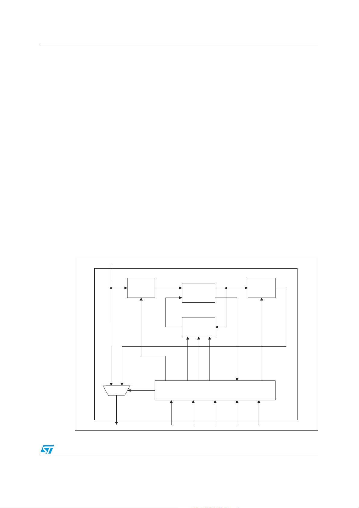
3.5 Group and block synchronization module
The group and block synchronization module has the following features:
– Hardware group and block synchronization
– Hardware error detection
– Hardware error correction, using quality bit information to indicate bad corrections
– Hardware synchronization flywheel
– TA, TAEON information extraction
– Reset by software “ar_res”, which resets also RAM buffer addresses and RDS
demodulator
Figure 5. Group and block synchronization diagram
RDSCLK
RDSDAT
RDSQAL
from RDS
Demodulator
BLOCK A
BLOCK B
BLOCK D
AR_RES
TAEON
TA
Group & Block Synchronization Control Block
rds_bd_h,rds_bd_l
read only read only read only
RDSDAT(15:0)
Syndrome register
S(9:0)
Correction
logic
Quality bit counter
RDS block counter
S(4:0)
Correct. pat.
rds_corrp rds_qu
CP(9:5)
Corrected
Data_OK
Syndrom zero
ABH
DBH
BLOCK E detected
Block
missed
Q(3:0)
QU(0:3)
new
next
Block
RDS
bit
available
rds_int
res
BLOCK A
BLOCK B
synch.
AR_RES
set set
read/write
BLOCK D
intbit_int
TAEON
TA
This module is used to acquire group and block synchronization of the received RDS data
stream, which is provided in a modified shortened cyclic code. For theory and
implementation of modified shortened cyclic code and error correction, please refer to
CENELEC Radio Data System (RDS) specification EN50067.
Group and block synchronization module can detect and correct five bit error burst in the
data stream. If an error correction is done on a good quality marked RDS bit, the “data_ok”
bit rds_corrp[1] won’t be set (refer to page 22). Before error correction, the five MSBs of the
syndrome register are stored in the “cp” bits rds_corrp[7:3].
If the five LSBs of the syndrome register are zero, the “cp” pattern is used for error
correction. After that operation the syndrome must become zero for valid RDS data. The
14/36 Doc ID 12064 Rev 4
Page 15

TDA7333N Functional description
type of error can be measured with the five “cp” bits in order to classify the reliability of the
correction. Each bit set within “cp” means that one bit was corrected.
The two RDS data bytes rds_bd_h[7:0] and rds_bd_l[7:0] are available at the I
2
C/SPI
interface together with status bits rds_corrp[7:0] and rds_qu[7:0] giving reliability information
of the data (refer to Figure 5). rds_int[7:0] bits are used for interrupt and group and block
synchronization control. A software reset “ar_res” rds_int[5] can be used to force
resynchronization.
An endless 2 bit block counter (A, B, C or C’, D, A, B...) increments one step if a new RDS
block was received. During synchronization the block counter is set to the first identified
valid RDS block. Then every next RDS block must be of that type which is indicated by the
block counter “blk” rds_qu[3:2]. If this is not true, then the syndrome becomes not zero
(indicated by “synz” bit rds_qu[0]) and the “data_ok” bit rds_corrp[1] is not set. In case of
USA BRDS, four consecutive E blocks can be received which are indicated by the “e” bit
rds_qu[1].
The quality bit counter rds_qu[7:4] counts the bad quality marked RDS bits within a RDS
block.
The group and block synchronization module extracts also TA, TAEON information and
detects blocks types A, B, D (refer to page 21) which can be used as interrupt sources.
The TA interrupt is performed in two cases: If within block B the group 0A or 0B is indicated
and the TA bit is set or if within block B group 15B is indicated and the TA bit is set. The
TAEON interrupt is performed, if within block B group 14B is indicated and the TA bit is set.
The interrupts can be recognized on the interrupt flag “int” rds_int[0] (refer to Section 3.8.1).
The external open drain pin INTN (15) is the inverted version of the “int” flag.
Doc ID 12064 Rev 4 15/36
Page 16

Functional description TDA7333N
3.6 Flywheel mechanism
Figure 6. Example for flywheel mechanism
100
Signal
quality [%]
1.) 2.) 3.)
63(max)
Flywheel
counter
synch
data_ok
bne
interrupt
0
0
1
0
1
0
time
time
time
time
time
Within group and block synchronization control block a 6 bit (64 states) flywheel counter is
implemented to control RDS synchronization. After reset or a forced resynchronization by
setting “ar_res” bit rds_int[5], this counter increments from zero to one, if a valid RDS block
was detected. Valid means the syndrome has to be zero (“synz” = 1 rds_qu[0]) without any
error corrections done on good quality marked RDS bits. Then the RDS module is
synchronized. This is indicated by “synch” bit rds_int[4] which is set if the flywheel counter is
greater than zero. Every valid consecutive RDS block (A, B, C or C’, D, A, B...) increments
the flywheel counter by two.
If the next consecutive RDS block has its syndrome not zero, or corrections are done on
good quality marked RDS bits, then the flywheel counter decrements by one. If the flywheel
counter becomes zero, then a new RDS block synchronization will be performed. If blocks of
type E are detected (indicated by “e” bit rds_qu[1]), then the flywheel counter will be not
modified, because in case of European RDS, block E is an error but not in case of USA
BRDS. This means E blocks are treated as neutral in this RDS/BRDS implementation.
The “data_ok” bit rds_corrp[1] is set only, if the flywheel counter is greater than two, the
syndrome of the detected RDS block is zero and if no error corrections are done on good
quality marked RDS bits.
Figure 6 shows an example for the flywheel mechanism.
The first diagram shows the relative signal quality of 26 received RDS bits. 100 % means
that the last received 26 RDS bits are all marked as good by the demodulator and 0% that
all are marked as bad.
16/36 Doc ID 12064 Rev 4
Page 17

TDA7333N Functional description
The second diagram gives information about the flywheel counter status. The counter value
could be between 0 and 63.
The next two charts showing the bits “synch” rds_int[4] and “data_ok” rds_corrp[1] (refer to
Section 3.8.1 and Section 3.8.3).
The last graph indicates every generated buffer not empty (bne) interrupt. After each
interrupt the RDS data will be read out from the RAM buffer (within 22 ms), before next RDS
block is written into. This is done to reset the interrupt flag “int” rds_int[0] each time. Further
the “syncw” bit rds_bd_ctrl[0] is set to one, to store only synchronized RDS blocks (refer to
Section 3.8.6).
The following case is considered now: First the receiving condition is good (section 1), then
it is going to be worse (section 2) because of entering a tunnel, after leaving it is going to be
better again (section 3).
Section 1: After power up or resynchronization (“ar_res”, rds_int[5]), the first recognized
RDS block is stored in the RAM buffer and generates an “bne” interrupt. At the same time
“synch” bit rds_int[4] is set to one. With the next stored RDS block the “data_ok” bit
rds_corrp[1] is set, because the flywheel counter becomes greater than two. With every next
RDS block the flywheel counter increments by two, until the upper margin of 63 is reached.
Section 2: Because of entering a tunnel, the demodulator increases bad marked RDS bits
until all are marked as bad. The flywheel counter decrements by one after each new RDS
block because of error corrections done on good marked RDS bits or because the
syndrome of the expected block was not zero after error correction. The “data_ok” bit
rds_corrp[1] is set to zero whenever the flywheel counter decrements. Note that the
synchronization flag “synch” rds_int[4] is set and the interrupt is performed after every
expected RDS block, until the flywheel counter is zero. Then the RDS is desynchronized.
Now spurious interrupts could occur because of random RDS blocks detected during
resynchronization process. If the time of receiving bad signal is shorter than the decreasing
time of the flywheel counter, then the RDS will keep its synchronization and stores RDS
data every 22 ms.
Section 3: After leaving the tunnel, the signal is getting better and the RDS will be
synchronized again as described in section 1.
Doc ID 12064 Rev 4 17/36
Page 18

Functional description TDA7333N
3.7 RAM Buffer
The RAM buffer can store up to 24 RDS blocks (rds_bd_h[7:0] and rds_bd_l[7:0]) with their
related information (rds_qu[7:0] and rds_corrp[7:0]) (Figure 7):
Figure 7. RAM buffer usage
INTERNAL REGISTERS
read access
(internal)
SA_DATAOUT
(spi mode)
SDA_DATAIN
(i2c mode)
rds_qu[7..0] rds_corrp[7..0] rds_bd_h[7..0] rds_bd_l[7..0] rds_bd_ctrl[7..0] sinc4reg[7..0] testreg[7..0]rds_int[7..0]
write access
(external)
RAM BUFFER
(24 blocks)
pllreg4[7..0]
pllreg0[7..0]
I2C/SPI SHIFT REGISTER
rds_int[7..0]
rds_qu[7..0] rds_corrp[7..0] rds_bd_h[7..0] rds_bd_l[7..0] rds_bd_ctrl[7..0]
sinc4reg[7..0] testreg[7..0]
pllreg4[7..0]
pllreg0[7..0]
After power up, or after resynchronization by setting “ar_res” rds_int[5] to one, incoming
RDS blocks are stored in the RAM buffer when synchronization has been established
(Figure 8). But if the bit “syncw” rds_bd_ctrl[0] (refer to Section 3.8.6) is cleared, every
received RDS block is stored, also without synchronization. This means if the RDS is not
synchronized, every received consecutive 26 RDS data bits are treated as a RDS block.
Figure 8. RAM buffer update depends on “syncw” bit rds_bd_ctrl[0]
Synchro-
"synch"
Buffer if
Buffer if
RDS data
bits
1
0
Block A Block B Block C
nization flag
Write to RAM
"syncw" = 1
Write to RAM
"syncw" = 0
18/36 Doc ID 12064 Rev 4
time
time
time
time
Page 19

TDA7333N Functional description
The RAM buffer is used as a circular FIFO (Figure 9). If more than 24 blocks are written, the
oldest data will be overwritten. One level of the buffer consists of 4 bytes (2 information
bytes, 2 RDS data bytes). If less than 4 bytes of the RAM buffer are read out from the
master via the SPI or I
2
C interface, the buffer address will not be incremented.
Figure 9. RAM buffer states
Rp
22
bne = 1
bfull = 0
bovf = 0
Wp
0
23
1
2
Wp
3
read
21
22
bne = 1
bfull = 0
bovf = 0
Rp
0
23
1
2
0
Rp
3
Wp
Rp Wp
13 4
0
21
22
bne = 0
bfull = 0
bovf = 0
23
write
1
2
2
21
22
bne = 0
bfull = 0
bovf = 0
Rp Wp
23
0
write
1
2
1
21
read
0
01
1
write next three data into
Rp
2
3
21
the read pointer doesn't go
reset status
write
5
21
the write pointer reaches position
before the read pointer
(24 data written before any read)
Note : The read pointer Rp is driven externally through micro read access,
and the write pointer Wp is driven internally on every incoming block.
Rp
Wp
0
23
1
1
6
Rp Wp
22
21
the read pointer reaches but
doesn't go ahead the write pointer
read
22
bne = 1
bfull = 0
bovf = 0
2
3
23
bne = 1
bfull = 0
bovf = 0
write the first data
into buffer (internally)
Wp
write
0
1
2
3
0
Wp
23
22
21
bne = 1
bfull = 1
bovf =
the Wp reaches Rp
overflow flag is set
and the first data is
overwritten
Rp
buffer (internally)
22
21
write
Wp and Rp are
moving together
overwriting next data
Rp Wp
0
23
22
bne = 0
bfull = 0
bovf = 0
ahead the write pointer
1
Wp
23
bne = 1
bfull = 1
bovf =
2
3
read three data from buffer
Rp
0
1
2
3
1
(externally)
Wp
Rp
The different states of the buffer are indicated with the help of following flags:
– “bne”, buffer not empty. It is set as soon as one RDS block is written in the buffer,
and reset when reading rds_int register. This flag is a bit of rds_int register, it is
also an interrupt source (refer to Section 3.8.1).
– “bfull”, buffer full. It is set when 24 RDS blocks have been written, that is to say that
there is about 20 ms to read out the buffer content before an overflow occurs. This
flag is an interrupt source.
– “bovf”, buffer overflow. It is set if more than 24 RDS blocks are written. This flag is
a bit of register rds_corrp (refer to Section 3.8.3) and is cleared only by reading
the whole buffer (24 blocks).
An address reset of the RAM buffer can be performed by writing a 1 to “ar_res” bit in rds_int
register, it also forces a resynchronization.
Doc ID 12064 Rev 4 19/36
Page 20

Functional description TDA7333N
Figure 9 describes the different states of the buffer with corresponding flags values:
1. This is the reset state, read (Rp) and write pointer (Wp) pointing at the same location 0.
The buffer is empty.
2. After the first buffer write operation, Wp points to the last written data (0, it is not
incremented) and the flag “bne” (buffer not empty) is set.
3. After next buffer write operation, Wp points to the last written data (3, incremented
address).
4. After buffer read operation, Rp points to incremented address (data to be read on the
next read cycle), following the Wp. As soon as Rp reaches the Wp (of value 3), it is not
incremented to 4 and flag “bne” is reset. Rp never goes ahead the Wp.
5. If the buffer is full (i.e. 24 blocks have been written before any read), flag “bfull” is set. If
no read operation is performed, on next write operation “bovf” (buffer overflow) is set,
and each subsequent write operation will overwrite the oldest data of the RAM buffer.
Rp is moved in front of the Wp.
6. If the whole content of the buffer has already been read, subsequent read operation will
always read the last written location - Rp never goes ahead the Wp.
3.8 Programming through serial bus interface
The serial bus interface is used to access the different registers of the chip. It is able to
handle both I
2
C and
SPI transfer protocols, the selection between the two modes is done thanks to the pin CSN:
– if the pin CSN is high, the interface operates as an I
2
C bus.
– if the pin CSN is asserted low, the interface operates as a SPI bus.
In both modes, the device is a slave, i.e the clock pin SCL_CLK is only an input for the chip.
Depending on the transfer mode, external pins have alternate functions as following:
Table 6. External pins alternate functions
Pin Function in SPI mode (CSN=0) Function in I2C mode (CSN=1)
SCL_CLK CLK (serial clock) SCL (serial clock)
SDA_DATAIN DATAIN (data input) SDA (data line)
SA_DATAOUT DATAOUT (data output) SA (slave address)
13 registers are available with read or read/write access:
Table 7. Registers description
Register
rds_int[7:0] (see 3.8.1) read/write interrupt source setting, synch., bne information
rds_qu[7:0] (see 3.8.2) read quality counter, actual block name
Access
rights
Function
rds_corrp[7:0] (see 3.8.3) read error correction status, buffer ovf information
rds_bd_h[7:0] (see 3.8.4) read high byte of current RDS block
rds_bd_l[7:0] (see 3.8.5) read low byte of current RDS block
20/36 Doc ID 12064 Rev 4
Page 21

TDA7333N Functional description
Table 7. Registers description (continued)
Register
rds_bd_ctrl[7:0] (see 3.8.6) read/write frequency, quality sensitivity, demodulator pll settings
sinc4reg[7:0] (see 3.8.7) read/write sinc4 filter settings (for internal use only)
testreg[7:0] (see 3.8.8) read/write test modes (for internal use only)
pllreg4[7:0] (see 3.8.9) read/write PLL control register 4
pllreg3[7:0] (see 3.8.10) read/write PLL control register 3
pllreg2[7:0] (see 3.8.11) read/write PLL control register 2
pllreg1[7:0] (see 3.8.12) read/write PLL control register 1
pllreg0[7:0] (see 3.8.13) read/write PLL control register 0
The meaning of each bit is described below:
3.8.1 rds_int register
Figure 10. rds_int registe
rds_int
reset value
bit name
access
(1)
bit 7 bit 0bit 1bit 2bit 3bit 4bit 5bit 6
interrupt source
no interrupt
buffer not empty
buffer full
block A
block B
block D
TA
TA EON
00
itsrc2
r/w r/w
itsrc200itsrc1
001
100
101
010
011
110
111
Access
rights
itsrc0 intar_resbne itsrc1synchwrite
itsrc0
0
r/w
Function
00000
0
Interrupt bit. It is set to one on every programmed interrupt. It is
reset by reading rds_int register. The inverted version is also
externally available on RDSINT pin.
rr/w r r/w r
itsrc[2:0] selects interrupt source (1).
Block A, B, D and TA, TA EON interrupts only if "synch" =1.
Synchronization information (refer to pages 13-15).
1: The module is already synchronized.
0: The module is synchronizing.
It is used to force a resynchronization. If it is set to one, the RDS
modules are forced to resynchronization state and the RAM buffer
address is reset.
This bit is reset automatically. It is read always as zero.
Buffer not empty.
1: At least one block is present in the RAM buffer.
0: The RAM buffer is empty.
rds_int, rds_bd_ctrl and pllreg4-0 write order.
This bit is only used in SPI mode and is read always as zero.
1: Update of rds_int, rds_bd_ctrl and pllreg4-0 with data shifted in.
0: No update of rds_int, rds_bd_ctrl and pllreg4-0.
(1) If the interrupt source is changed form block A, B,
D, TA, TA EON to another one "no interrupt" must be
set before to clear the previous interrupt acknowledge.
Doc ID 12064 Rev 4 21/36
Page 22

Functional description TDA7333N
3.8.2 rds_qu register
Figure 11. rds_qu register
rds_qu
reset value
bit 7 bit 0bit 1bit 2bit 3bit 4bit 5bit 6
0
00
bit name
r
access
(2)
rr
block name
block A
block B
block D
3.8.3 rds_corrp register
000
rrr
blk1
blk0
00
10
1block C,C' 0
11
0
0
synzequ0qu3 qu1qu2 blk1 blk0
r
r
It indicates if error correction was successful.
1: The syndrome was zero after error correction.
0: The syndrome did not become zero and therefore the error
correction was not successful.
1: Block E is detected. This indicates a paging block which is
deÞned in the RBDS speciÞcation used in the United States of
America.
0: An ordinary RDS block A, B, C, C« or D is detected, or no valid
syndrome was found.
Bit 0 of block counter (2).
bit 1 of block counter (2).
bit 0 of quality counter
bit 1 of quality counter
bit 2 of quality counter (3).
bit 3 of quality counter (3).
(3).
(3).
(2) If "syncw" =1 of rds_bd_ctrl register, the block counter indicates the expected RDS block.
(3) qu[3...0] counts the number of bits (max.16) which are
marked as bad by the demodulator within each RDS block.
It could be used as a quality information, indicating the maximum number of bits which are allowed to be corrected.
Figure 12. rds_corrp register
rds_corrp
reset value
bit name
access
bit 7 bit 0bit 1bit 2bit 3bit 4bit 5bit 6
0
00
r
rr
000
rrr
0
0
Buffer overflow
bovfdat_okcp6cp9 cp7cp8 cp5 correct
1: More than 24 blocks have been written into the buffer.
r
r
0: No buffer data has been overwritten.
Information if the current RDS data could be used.
1: A correct syndrome was detected and no error correction was
done on a good quality marked RDS bit and the flywheel counter is
greater than 2 (RDS data is OK).
0: The syndrome was wrong, or an error correction was done on a
good quality marked RDS bit, or the flywheel counter is lower than 3
(RDS data is not OK).
It is an information about error correction.
1: An error correction was done.
0: The actual RDS block is detected as error free.
bit 5 of the syndrome register(4).
bit 6 of the syndrome register(4).
bit 7 of the syndrome register(4).
bit 8 of the syndrome register(4).
bit 9 of the syndrome register(4).
(4) (Refer to CENELEC Radio Data System speciÞcation
EN50067, ANNEX B). When bits 0...4 of the syndrome register are zero, a possible error burst is detected. With help
of the correction pattern (bits 5...9 of the syndrome register),
the type of error can be measured, in order to classify the
reliability of the correction.
22/36 Doc ID 12064 Rev 4
Page 23

TDA7333N Functional description
3.8.4 rds_bd_h register
Figure 13. rds_bd_h registe
rds_bd_h
reset value
bit 7 bit 0bit 1bit 2bit 3bit 4bit 5bit 6
0
00
bit name
r
access
rr
3.8.5 rds_bd_l register
Figure 14. rds_bd_l register
rds_bd_l
reset value
bit name
access
bit 7 bit 0bit 1bit 2bit 3bit 4bit 5bit 6
0
00
r
rr
000
rrr
000
rrr
0
r
0
r
0
m8m9m12m15 m13m14 m11 m10
r
bit 15 of the actual RDS 16 bits information.
bit 14 of the actual RDS 16 bits information.
bit 13 of the actual RDS 16 bits information.
bit 12 of the actual RDS 16 bits information.
bit 11 of the actual RDS 16 bits information.
bit 10 of the actual RDS 16 bits information.
bit 9 of the actual RDS 16 bits information.
bit 8 of the actual RDS 16 bits information.
0
m0m1m4m7 m5m6 m3 m2
r
bit 7 of the actual RDS 16 bits information.
bit 6 of the actual RDS 16 bits information.
bit 5 of the actual RDS 16 bits information.
bit 4 of the actual RDS 16 bits information.
bit 3 of the actual RDS 16 bits information.
bit 2 of the actual RDS 16 bits information.
bit 1 of the actual RDS 16 bits information.
bit 0 of the actual RDS 16 bits information.
Doc ID 12064 Rev 4 23/36
Page 24

Functional description TDA7333N
3.8.6 rds_bd_ctrl register
Figure 15. rds_bd_ctrl register
rds_bd_ctrl
reset value
bit name
access
(5)
pllf
0
1
(6)
pllb1
10
bit 7 bit 0bit 1bit 2bit 3bit 4bit 5bit 6
0
00
r/w
r/w r/w
lock time needed for 90 deg deviation
pllb0
00
10
11
000
r/w r/w r/w
2 ms
10 ms
lock time needed for 90 deg deviation
5 ms (reset status)
15 ms
35 ms
76 ms
1
0
shw syncwpllb1freq qsens0qsens1 pllb0 pllf
r/w
Write into buffer if synchronized (refer to page 10-12) (8)
r/w
1: Write into buffer only if synchronized (reset value).
0: Write into buffer any incoming RDS block.
Select PLL time constants by software or hardware (8)
1: Software. Time constants are selected by pllb[1:0] respectively
pllf.
0: Hardware (reset value). Time constants automatically increase
after reset or resynchronization.
Set the 57 kHz pll time constant (5) (8).
Bit 0 of 1187.5 Hz pll time constant (6) (8).
Bit 1 of 1187.5 Hz pll time constant (6) (8).
Bit 0 of quality sensitivity (7) (8).
Bit 1 of quality sensitivity (7) (8).
Select internal master clock frequency (fsys):
1: 8.664 MHz.
0: 8.55 MHz (reset value).
(7) Select sensitivity of quality bit.
00: minimum (reset value)
11: maximum
(8) Bit 5 "ar_res" of rds_int register will clear the bits 06 of the rds_bd_ctrl register.
3.8.7 sinc4reg register
Figure 16. sinc4reg register
sinc4reg
reset value
bit name
access
bit 7 bit 0bit 1bit 2bit 3bit 4bit 5bit 6
0
r/w
r/w r/w
00
3.8.8 testreg register
Figure 17. testreg register
testreg
reset value
bit name
access
bit 7 bit 0bit 1bit 2bit 3bit 4bit 5bit 6
0
00
r/w
r/w r/w
000
r/w r/w r/w
000
r/w r/w r/w
0
0
r/w
0
r/w
sinc4reg register is for internal use only. For application this register
--------
must be always Þlled with zeros.
r/w
0
testreg register is for internal use only. For application this register
--------
must be always Þlled with zeros.
r/w
24/36 Doc ID 12064 Rev 4
Page 25

TDA7333N Functional description
3.8.9 pllreg4 register
Figure 18. pllreg4 register
pllreg4
reset value
bit 7 bit 0bit 1bit 2bit 3bit 4bit 5bit 6
0
00
bit name
access
r
3.8.10 pllreg3 register
Figure 19. pllreg3 register
011
PWDN TEST1 TEST0
r r/w
r/w r/w r/w
0
0
FRAENLOCK PLLENLLOCK DITEN
r/w
r/w
This bit is for internal test only.
This bit is for internal test only.
PLL factional mode enable (10).
1: Fractional mode enabled.
0: Fractional mode disabled.
PLL fractional dither enable (10).
1: Fractional dither enabled.
0: Fractional dither disabled.
Power down mode.
0: Normal mode
1: Power down mode. All clocks are stopped. This mode can only
be exit by hardware reset.
PLL enable. If this bit is set the PLL will be initialized with the values
of the pllreg4-0 registers. After PLL locking, the system clock (fsys)
is switched to the PLL output clock which must be 8.55 or 8.664
MHz. Clearing this bit will switch fsys back to the XTI clock.
PLL lost lock.
This bit is set if the PLL is used and loses lock. It will be cleared if
the PLL is disabled and enabled again.
PLL lock.
1: PLL is currently locked.
0: PLL is currently out of lock.
pllreg3
reset value
bit name
access
bit 7 bit 0bit 1bit 2bit 3bit 4bit 5bit 6
0
IDF4
r
00
IDF3
r/w r/w
001
IDF2-
IDF1 IDF0
r/w r/w r/w
0
1
ODF3ODF4
r/w
r/w
bit 3 of PLL output divide factor (9) (10) (12).
bit 4 of PLL output divide factor (9) (10) (12).
bit 0 of PLL input divide factor (10) (12).
bit 1 of PLL input divide factor (10) (12).
bit 2 of PLL input divide factor (10) (12).
bit 3 of PLL input divide factor (10) (12).
bit 4 of PLL input divide factor (10) (12).
Not used.
Doc ID 12064 Rev 4 25/36
Page 26

Functional description TDA7333N
3.8.11 pllreg2 register
Figure 20. pllreg2 register
pllreg2
reset value
bit name
access
bit 7 bit 0bit 1bit 2bit 3bit 4bit 5bit 6
1
ODF1
r/w
11
r/w r/w
3.8.12 pllreg1 register
Figure 21. pllreg1 register
pllreg1
reset value
bit name
access
bit 7 bit 0bit 1bit 2bit 3bit 4bit 5bit 6
1
r/w
10
r/w r/w
010
MF6ODF3
ODF0
r/w r/w r/w
000
FRA12MF1 FRA13MF0
r/w r/w r/w
MF5 MF4
FRA11 FRA10
1
0
r/w
(9) ODF value equal to zero is ignored, one is then used.
MF2MF3
r/w
bit 2 of PLL multiplication factor (10) (11) (12).
bit 3 of PLL multiplication factor (10) (11) (12).
bit 4 of PLL multiplication factor (10) (11) (12).
bit 5 of PLL multiplication factor (10) (11) (12).
bit 6 of PLL multiplication factor (10) (11) (12).
bit 0 of PLL output divide factor (9) (10) (12).
bit 1 of PLL output divide factor (9) (10) (12).
bit 2 of PLL output divide factor (9) (10) (12).
(10) Reset values are designed for 10.25 MHz XTI input frequency.
0
1
FRA8FRA9
r/w
r/w
bit 8 of fractional factor (10) (12).
bit 9 of fractional factor (10) (12).
bit 10 of fractional factor (10) (12).
bit 11 of fractional factor (10) (12).
bit 12 of fractional factor (10) (12).
bit 13 of fractional factor (10) (12).
bit 0 of PLL multiplication factor (10) (11) (12).
bit 1 of PLL multiplication factor (10) (11) (12).
(11) MF values smaller than 9 are ignored, 9 is then
used internally.
3.8.13 pllreg0 register
Figure 22. pllreg0 register
pllreg0
reset value
bit name
access
26/36 Doc ID 12064 Rev 4
bit 7 bit 0bit 1bit 2bit 3bit 4bit 5bit 6
1
r/w
00
r/w r/w
000
FRA4FRA7 FRA5FRA6
FRA3 FRA2
r/w r/w r/w
0
0
FRA0FRA1
r/w
r/w
bit 0 of fractional factor (10).
bit 1 of fractional factor (10).
bit 2 of fractional factor (10)
bit 3 of fractional factor (10).
bit 4 of fractional factor (10).
bit 5 of fractional factor (10).
bit 6 of fractional factor (10).
bit 7 of fractional factor (10).
(12) The registers pllreg3, pllreg2 and pllreg1 must be
written at once to be updated, i.e. if the I2C/SPI stops
after pllreg2, then these registers are not updated.
Page 27

TDA7333N Functional description
Note: sinc4reg and testreg registers are dedicated for testing and are not described in this
specification.
Reset values of rds_qu, rds_corrp, rds_bd_h and rds_bd_l registers are not visible for the
programmer, because he can see only the copy of this registers in the RAM buffer after a
new RDS block was received.
The pllreg4-0 registers must be initialized first, before the RDS functionality can be used. If
the “PLLEN” bit of pllreg4 is set from zero to one, then the PLL will be initialized after
2
I
C/SPI transfer with the actual values of pllreg4-0. After the lock time the PLL switches
automatically over to the PLL output clock. The next I
2
C/SPI transfer is only allowed after the
lock time (500 µs) and additional 25 XTI input clock cycles. If the “PLLEN” bit is set from one
to zero, the PLL will be stopped and the system clock is switched back to the XTI input clock
(after the I
clock cycles. This is to avoid any I
2
C/SPI transfer). The next I2C/SPI transfer is then only allowed after 25 XTI input
2
C/SPI communication during clock switching.
The registers pllreg3-1 can be only changed at once. If there are less then all three pllreg3-1
registers written during a I
If the XTI input frequency is 10.25 MHz, then only register pllreg4 must be programmed,
because the pllreg3-0 register reset values can be used without any modification.
3.9 I2C transfer mode
This interface consists of three lines: a serial data line (SDA), a bit clock (SCL), and a slave
address select (SA).
The interface is capable of operating up to 400 kbits/s. If during the setup the system clock
fsys is smaller then 8.55 MHz, then the max. I
MHz then the maximum I
Data transfers follow the format shown in Figure 23. After the START condition (S), a slave
address is sent. The address is 7 bits long followed by an eighth bit which is a data direction
bit (R/_W).
A zero indicates a transmission (WRITE), a one indicates a request for data (READ).
The slave address of the chip is set to 001000S, where S is the least significant bit of the
slave address set externally via the pin SA_DATAOUT. This allows to choose between two
addresses in case of conflict with another device of the radio set.
Each byte has to be followed by an acknowledge bit (SDA low).
2
C/SPI transfer, then they will be not updated.
2
2
C speed is 200 kbits/s for setup).
C speed decreases linear (e.i. if fsys = 4.275
Data is transferred with the most significant (MSB) bit first.
A data transfer is always terminated by a stop condition (P) generated by the master.
Figure 23. I
2
C data transfer
SDA
SCL
S P
START
CONDITION
1-7 8
ADDRESS R/W ACK DATA ACK DATA
9 1-7 8
Doc ID 12064 Rev 4 27/36
9
1-7 8
9
ACK/ACK
CONDITION
STOP
Page 28

Functional description TDA7333N
3.9.1 Write transfer
Figure 24. I2C write transfer
S Slave address rds_int AA A sinc4reg A PW testreg
rds_bd_ctrl
A
S = start condition
W = write mode
from master to slave
from slave to master
Slave address = 001000S ( where S is the level of the pin
SA_DATAOUT)
A = acknowledge bit
P = stop condition
9 registers are available with write access (please refer to Section 3.8 for the meaning of
each bit).
To write registers, the external master must initiate the write transfer as described above,
then send the data to be written, and terminate the transfer by generating a stop condition.
The transfer can be terminated after having written one, two, three, four (Figure 24), or five
bytes.
The registers are written in the following order:
rds_int[7:0], rds_bd_ctrl[7:0], sinc4reg[7:0], testreg[7:0], pllreg4[7:0], pllreg3[7:0],
pllreg2[7:0], pllreg1[7:0], pllreg0[7:0].
sinc4reg[7:0] and testreg[7:0] are dedicated for test and have to keep zero filled for
application.
Figure 25. I
2
C write operation example: write of rds_int and rds_bd_ctrl registers
SA
0
1
CSN
SDA
SCL
S
START
CONDITION
SLAVE ADDRESS
3.9.2 Read transfer
Figure 26. I2C read transfer
from master to slave
from slave to master
rds_bd_ctrl[7:0]
W ACK
rds_int[7:0]
ACK ACK
RS Slave address rds_int A rds_quA A testreg A P
S = start condition
R = read mode
Slave address = 001000S ( where S is the level of the pin
SA_DATAOUT)
A = acknowledge bit
P = stop condition
P
STOP
CONDITION
28/36 Doc ID 12064 Rev 4
Page 29

TDA7333N Functional description
13 bytes can be read at a time (please refer to Section 3.8 for the meaning of each bit).
The master has the possibility to read less than 13 registers by not sending the
acknowledge bit and then generating a stop condition after having read the needed amount
of registers.
There are two typical read access:
– read only the first register rds_int to check the interrupt bit.
– read the first five registers rds_int, rds_qu, rds_corrp, rds_bd_h and rds_bd_l to
get the RDS data.
The registers are read in the following order:
rds_int[7:0], rds_qu[7:0], rds_corrp[7:0], rds_bd_h[7:0], rds_bd_l[7:0], rds_bd_ctrl[7:0],
sinc4reg[7:0], testreg[7:0], pllreg4[7:0], pllreg3[7:0], pllreg2[7:0], pllreg1[7:0],
pllreg0[7:0].
Only the “bne” flag can be used for polling mode. There are two different ways to use this
mode, while the first one causes less bus traffic than the second:
1. Read only the first register rds_int to check the “bne” bit.
If “bne” bit is not set, the stop condition can be set, as shown in (Figure 28).
If “bne” bit is set, the transfer must be continued by the i2c master, until at least the four
register rds_qu, rds_corrp, rds_bd_h and rds_bd_l are read out, then the i2c master is
allowed to set the stop condition (Figure 27). Then the whole Buffer must be read out,
by reading each time at least the five registers rds_int, rds_qu, rds_corrp, rds_bd_h
and rds_bd_l without interruption. This must be done until the “bne” bit is set to zero
(last RDS block).
2. If the I
2
C master is not able to handle the above protocol, it must read always at least
the first five registers rds_int, rds_qu, rds_corrp, rds_bd_h, rds_bd_l out independent if
“bne” is set or not (Figure 27). If the “bne” flag is set the whole RAM buffer must be
read out, by reading each time at least the five registers rds_int, rds_qu, rds_corrp,
rds_bd_h and rds_bd_l without interruption. This must be done until the “bne” bit is set
to zero (last RDS block).
Note: In polling mode the interrupt flag “int” is just a indication that the wanted information is stored
within the RAM Buffer.
In polling mode it is possible that the last RDS data (rds_qu, rds_corrp, rds_bd_h and
rds_bd_l), which was read out as the “bne” flag was set to zero, is identical to the RDS data
before. This must be checked by the external micro controller by comparing the last received
2 RDS blocks. If they are identical, one of them can be skipped. (This is the case if just one
RDS block is stored in the RAM buffer).
Figure 27. I
SA
0
1
CSN
SDA
SCL
S
START
CONDITION
2
C read access example 1: read of 5 bytes
rds_qu[7:0]
ACK ACK
SLAVE ADDRESS
rds_int[7:0]
R ACK
Doc ID 12064 Rev 4 29/36
rds_corrp[7:0]
rds_bd_h[7:0]
ACK ACK ACK
rds_bd_l[7:0]
P
STOP
CONDITION
Page 30

Functional description TDA7333N
S
N
Figure 28. I2C read access example 2: read of 1 byte
SA
0
1
SN
DA
SCL
START
CONDITION
S
SLAVE ADDRESS
R ACK
rds_int[7:0]
P
ACK
STOP
CONDITIO
3.10 SPI Mode
Figure 29. SPI data transfer
CSN
CLK
DATAIN
DATAOUT
t
csutsu
update of
shiftregister with
registers content
t
h
t
odvtoh
2
rds_int[7] testreg[0]rds_int[6] rds_int[0]rds_int[1]rds_int[2]rds_int[3]rds_int[4]rds_int[5] testreg[1]
shift of DATAIN
in shiftregister
tclt
ch
64638765431
rds_int[0]rds_int[1]
t
d
t
csh
update of registers
with shiftregister
content if requested
This interface consists of four lines (Figure 29). A serial data input (DATAIN), a serial data
output (DATAOUT), a chip select input (CSN) and a bit clock input (CLK).
The interface is capable of operating up to 1 MHz. If during the setup the system clock fsys
is smaller then 8.55 MHz, then the max. SPI speed decreases linear (e.i. if fsys = 4.275 MHz
then the maximum SPI speed is 500 kHz for setup).
CSN starts and stops the data transfer. After starting data transfer, one bit is shifted out
(DATAOUT) with the active bit clock edge (CLK) and at the same time one bit in (DATAIN).
When CSN stops the data transfer, the pllreg0[7:0], pllreg1[7:0] pllreg2[7:0], pllreg3[7:0],
pllreg4[7:0], rdstest[7:0], sinc4reg[7:0], rds_bd_ctrl[7:0], rds_int[7:0] registers can be
updated with the last bytes which have been shifted in.
The last byte shifted in on DATAIN must be always rds_int[7:0] and the last but one is
rds_bd_ctrl[7:0], and so on, as listed above. In other words, the master has take into
account the number of bytes to transfer before starting, to be sure that the last byte shifted in
at DATAIN is rds_int[7:0].
If the pllreg0[7:0], pllreg1[7:0] pllreg2[7:0], pllreg3[7:0], pllreg4[7:0], rdstest[7:0],
sinc4reg[7:0], rds_bd_ctrl[7:0], rds_int[7:0] registers will be updated depends on the MSB of
rds_int. If rds_int[7] = 1 all registers listed above are updated (refer to page 18). The
registers pllreg3-1 are only updated if they are shifted completely into the SPI.
sinc4reg[7:0] and testreg[7:0] are dedicated for test and have to be kept zero filled in the
application, independent if rds_int[7] bit is set or not.
30/36 Doc ID 12064 Rev 4
Page 31

TDA7333N Functional description
Only the “bne” flag can be used for polling mode. There are two different ways to use
polling mode, while the first one causes less bus traffic than the second:
1. Read only the first register rds_int to check the “bne” bit.
If “bne” bit is not set, the CSN can be set, as shown in (Figure 32).
If “bne” bit is set, the transfer must be continued by the SPI master, until at least the
four register rds_qu, rds_corrp, rds_bd_h and rds_bd_l are read out, then the SPI
master is allowed to stop the transfer by pulling CSN up. Then the whole Buffer must be
read out, by reading each time at least the five registers rds_int, rds_qu, rds_corrp,
rds_bd_h and rds_bd_l without interruption. This must be done until the “bne” bit is set
to zero (last RDS block).
2. If the SPI master is not able to handle the above protocol, it must read always at least
the first five registers rds_int, rds_qu, rds_corrp, rds_bd_h, rds_bd_l out independent if
“bne” is set or not. If the “bne” flag is set the whole RAM Buffer must be read out, by
reading each time at least the five registers rds_int, rds_qu, rds_corrp, rds_bd_h and
rds_bd_l without interruption. This must be done until the “bne” bit is set to zero (last
RDS block).
Note: In polling mode the interrupt flag “int” is just a indication that the wanted information is stored
within the RAM buffer.
In polling mode it is possible that the last RDS data (rds_qu, rds_corrp, rds_bd_h and
rds_bd_l), which was read out as the “bne” flag was set to zero, is identical to the RDS data
before. This must be checked by the external micro controller by comparing the last received
2 RDS blocks. If they are identical, one of them can be skipped (This is the case if just one
RDS block is stored within the RAM buffer).
Hereafter you can find typical read/write access in SPI mode:
Figure 30. Write rds_int, rds_bd_ctrl and pll_reg4 registers in SPI mode, reading
RDS data and related flags
CSN
CLK
DATAIN
DATAOUT
pll_reg4l[7:0]
rds_int[7:0] rds_qu[7:0] rds_corrp[7:0] rds_bd_h[7:0] rds_bd_l[7:0]
testreg[7:0]
sinc4reg[7:0]
{1,rds_int[6:0]}rds_bd_ctrl[7:0]
Figure 31. Read out RDS data and related flags, no update of rds_int and
rds_bd_ctrl registers
CSN
CLK
DATAIN
DATAOUT
{x,x,x,x,x,x,x,x}
rds_int[7:0] rds_qu[7:0] rds_corrp[7:0] rds_bd_h[7:0] rds_bd_l[7:0]
testreg[7:0]
sinc4reg[7:0]
{x,x,x,x,x,x,x,x}
{0,x,x,x,x,x,x,x}
Doc ID 12064 Rev 4 31/36
Page 32

Functional description TDA7333N
Note: sinc4reg and testreg must be zero filled for application.
Figure 32. Write rds_int registers in SPI mode, reading 1 register
CSN
CLK
DATAIN
DATAOUT
{1,rds_int[6:0]}
rds_int[7:0]
The content of the RDS registers is clocked out on DATAOUT pin in the following order:
rds_int[7:0], rds_qu[7:0], rds_corrp[7:0], rds_bd_l[7:0], rds_bd_h[7:0], rds_ctrl[7:0],
sinc4reg[7:0], testreg[7:0], pllreg4[7:0], pllreg3[7:0], pllreg2[7:0], pllreg1[7:0],
pllreg0[7:0].
For the meaning of each bit please refer to Section 3.8.
Note: 1 After 40 bit clocks the whole RDS data and flags are clocked out.
2 In SPI mode with applications having 2 or more SPI peripherals, it is necessary to inhibit the
clock line going to the TDA7333N when the CE line is kept high (not active).
32/36 Doc ID 12064 Rev 4
Page 33

TDA7333N Application notes
4 Application notes
4.1 Typical RDS data transfer
1. After power up the device, the PLL must be initialized and enabled to generate the
8.55 MHz or 8.664 MHz system clock (fsys). If the XTI frequency is already 8.55 MHz
or 8.664 MHz, this point can be skipped. If not, the pllreg4-0 register must be
programmed via I2C/SPI. If the XTI frequency is smaller then 8.55 MHz, the reduced
maximum I2C/SPI speed must be considered. After the pllreg4-0 register has been
programmed, 500 us and additional 25 XTI input clock cycles must be waited until the
PLL is locked and the system clock fsys is switched over to the PLL output clock. Then
the next I
8.55/8.664 MHz system clock (fsys).
2. In the next I2C/SPI transfer the interrupt source will be set to “buffer not empty”
(itsrc[2:0] = 001) and a resynchronization should be forced (rds_int[5] = 1), to be sure
that the buffer is empty and not filled with spurious RDS data. To do this only an write
access to the first register rds_int is needed.
3. Now the pin INTN must be continuously checked for an interrupt (active low). If there is
an interrupt the five registers rds_int, rds_qu, rds_corrp, rds_bd_h and rds_bd_l must
be read out to get the RDS data. The next interrupt can not be expected before 22 ms.
4. If it is not possible to service the interrupt in time, then the RDS buffer can store up to
24 RDS bocks. If the buffer is full and the data could not be read before the next RDS
block, the “buffer overflow” flag (rds_corrp[0] = 1) will be set. In this case at least one
RDS block is missed. The “buffer overflow” flag is only cleared, if the whole RDS buffer
is read out.
2
C/SPI transfer is allowed with its maximum speed specified for the
If there is no pin available for checking the INTN pin, then it is possible to read out the RDS
data by I
rds_int[6] bit is set, the 2C/SPI transfer must be continued, until at least the four register
rds_qu, rds_corrp, rds_bd_h and rds_bd_l are read out.
This must be done until rds_int[6] bit is set to zero (last RDS block). It is possible that the last
RDS block is the same as the last but one RDS block. This is the case if just one RDS block
was stored in the RAM buffer. If they are identical, one of them can be skipped.
If another interrupt source is used instead of “buffer not empty” for the INTN pin, also the
polling mode must be used for reading out the whole RDS buffer, as described above.
2
C/SPI polling. Only the “buffer not empty” flag (rds_int[6]) can be used for that. If
Doc ID 12064 Rev 4 33/36
Page 34

Package information TDA7333N
5 Package information
In order to meet environmental requirements, ST offers these devices in different grades of
ECOPACK
®
packages, depending on their level of environmental compliance. ECOPACK
®
specifications, grade definitions and product status are available at: www.st.com.
ECOPACK
®
is an ST trademark.
Figure 33. TSSOP16 mechanical data and package dimensions
DIM.
A 1.200 0.047
A1 0.050 0.150 0.002 0.006
A2 0.800 1.000 1.050 0.031 0.039 0.041
b 0.190 0.300 0.007 0.012
c 0.090 0.200 0.005 0.009
D (1) 4.900 5.000 5.100 0.114 0 .118 0.122
E 6.200 6.400 6.600 0.244 0.252 0.260
E1 (1) 4.300 4.400 4.500 0.170 0.173 0.177
e 0.650 0.026
L 0.450 0.600 0.750 0.018 0.024 0.030
L1 1.000 0.039
k 0˚ (min.) 8˚ (max.)
aaa 0.100 0.004
Note: 1. D and E1 does not include mold flash or protrusions.
mm inch
MIN. TYP. MAX. MIN. TYP. MAX.
Mold flash or potrusions shall not exceed 0.15mm
(.006inch) p er side.
OUTLINE AND
MECHANICAL DATA
TSSOP16
(Body 4.4mm)
34/36 Doc ID 12064 Rev 4
0080338 (Jedec MO-153-AB)
Page 35

TDA7333N Revision history
6 Revision history
Table 8. Document revision history
Date Revision Changes
06-Feb-2006 1 Initial release.
24-Jul-2006 2
09-Jun-2008 3 Added Note 2 on page 32.
23-Sep-2009 4
Document reformatted.
Modified function of the pin 6 on Ta bl e 2 .
Updated Figure 1: Block diagram and Figure 2: Pin connection (top
view).
Section 3.8: Programming through serial bus interface reformatted,
no content change.
Doc ID 12064 Rev 4 35/36
Page 36

TDA7333N
Please Read Carefully:
Information in this document is provided solely in connection with ST products. STMicroelectronics NV and its subsidiaries (“ST”) reserve the
right to make changes, corrections, modifications or improvements, to this document, and the products and services described herein at any
time, without notice.
All ST products are sold pursuant to ST’s terms and conditions of sale.
Purchasers are solely responsible for the choice, selection and use of the ST products and services described herein, and ST assumes no
liability whatsoever relating to the choice, selection or use of the ST products and services described herein.
No license, express or implied, by estoppel or otherwise, to any intellectual property rights is granted under this document. If any part of this
document refers to any third party products or services it shall not be deemed a license grant by ST for the use of such third party products
or services, or any intellectual property contained therein or considered as a warranty covering the use in any manner whatsoever of such
third party products or services or any intellectual property contained therein.
UNLESS OTHERWISE SET FORTH IN ST’S TERMS AND CONDITIONS OF SALE ST DISCLAIMS ANY EXPRESS OR IMPLIED
WARRANTY WITH RESPECT TO THE USE AND/OR SALE OF ST PRODUCTS INCLUDING WITHOUT LIMITATION IMPLIED
WARRANTIES OF MERCHANTABILITY, FITNESS FOR A PARTICULAR PURPOSE (AND THEIR EQUIVALENTS UNDER THE LAWS
OF ANY JURISDICTION), OR INFRINGEMENT OF ANY PATENT, COPYRIGHT OR OTHER INTELLECTUAL PROPERTY RIGHT.
UNLESS EXPRESSLY APPROVED IN WRITING BY AN AUTHORIZED ST REPRESENTATIVE, ST PRODUCTS ARE NOT
RECOMMENDED, AUTHORIZED OR WARRANTED FOR USE IN MILITARY, AIR CRAFT, SPACE, LIFE SAVING, OR LIFE SUSTAINING
APPLICATIONS, NOR IN PRODUCTS OR SYSTEMS WHERE FAILURE OR MALFUNCTION MAY RESULT IN PERSONAL INJURY,
DEATH, OR SEVERE PROPERTY OR ENVIRONMENTAL DAMAGE. ST PRODUCTS WHICH ARE NOT SPECIFIED AS "AUTOMOTIVE
GRADE" MAY ONLY BE USED IN AUTOMOTIVE APPLICATIONS AT USER’S OWN RISK.
Resale of ST products with provisions different from the statements and/or technical features set forth in this document shall immediately void
any warranty granted by ST for the ST product or service described herein and shall not create or extend in any manner whatsoever, any
liability of ST.
ST and the ST logo are trademarks or registered trademarks of ST in various countries.
Information in this document supersedes and replaces all information previously supplied.
The ST logo is a registered trademark of STMicroelectronics. All other names are the property of their respective owners.
© 2009 STMicroelectronics - All rights reserved
STMicroelectronics group of companies
Australia - Belgium - Brazil - Canada - China - Czech Republic - Finland - France - Germany - Hong Kong - India - Israel - Italy - Japan -
Malaysia - Malta - Morocco - Philippines - Singapore - Spain - Sweden - Switzerland - United Kingdom - United States of America
www.st.com
36/36 Doc ID 12064 Rev 4
 Loading...