

TDA7309
Fi
DIGITAL CONTROLLED STEREO AUDIO PROCESSOR
WITH LOUDNESS
1FEATURES
■ INPUT MULTIPLEXER:
3 STEREO INPUTS
■ RECORD OUTPUT FUNCTION
■ LOUDNESS FUNCTION
■ VOLUME CONTROL IN 1dB STEPS
■ INDEPENDENT LEFT AND RIGHT VOLUME
CONTROL
■ SOFT MUTE FUNCTION
■ ALL FUNCTIONS PROGRAMMABLE VIA
SERIAL I
2
C BUS
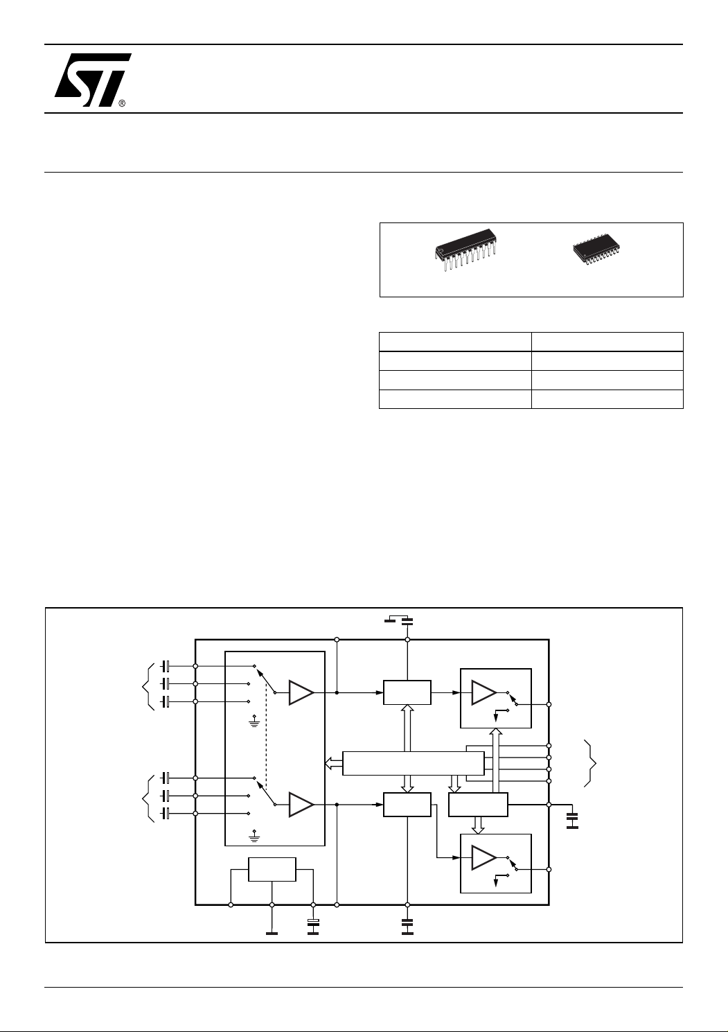
2 DESCRIPTION
The TDA7309 is a control processor with independent left and right volume control for quality audio
applications. Selectable external loudness and
soft mute functions are provided.
Control is accomplished by serial I
processor interface.
Figure 2. Block Diagram
2
C bus micro-
gure 1. Packages
DIP20
SO20
Table 1. Order Codes
Part Number Package
TDA7309 DIP20
TDA7309D SO20
TDA7309D013TR Tape & Reel
The AC signal setting is obtained by resistor networks and switches combined with operational
amplifiers.
Thanks to the used BIPOLAR/CMOS Technology,
Low Distortion, Low Noise and Low DC stepping
are obtained.
March 2006
LEFT
INPUTS
RIGHT
INPUTS
3 x
2.2µF
3 x
2.2µF
17
18
20
14
13
11
SELECTOR
SUPPLY
16 7 15
AGNDV
S
INPUT
CREF
Recout(L)
1
TDA7309
10
Recout(R)
22µF
LOUD(L)
LOUDNESS
LOUDNESS
LOUD(R)
19
VOLUME +
VOLUME +
12
100nF
100nF
SOFT
MUTE
MUTE
MUTE
2
6
4
5
8
3 CSM
9
D93AU045A
OUT
LEFT
DIGGND
SDA
SCL
ADDR
OUT
RIGHT
BUSSERIAL BUS DECODER + LATCHES
Rev. 6
1/14
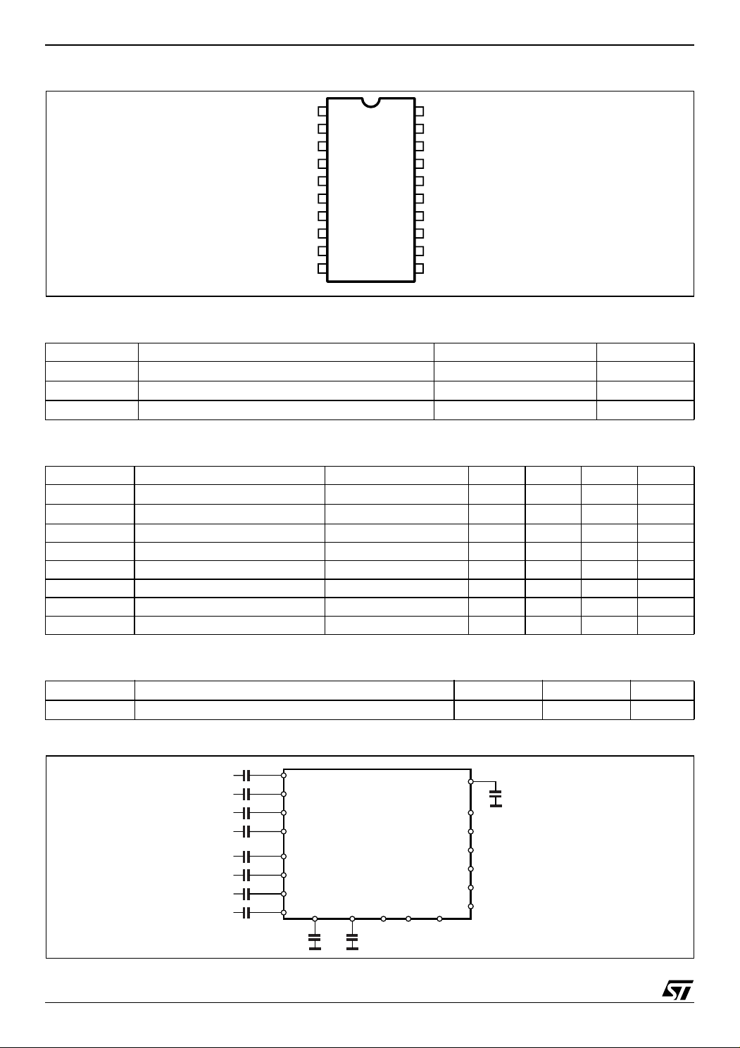
TDA7309
Figure 3. Pin Description
RecoutL
OUTL
CSM
SDA
SCL
DGND
GND
ADD
OUTR
1
2
3
4
5
6
7
8
9 LOUDR
IN3L20
LOUDL
19
IN2L
18
IN1L
17
V
16
15
14
13
S
CREF
IN1R
IN2R
12
RecoutR 10 IN3R11
D94AU058A
Table 2. Absolute Maximum Ratings
Symbol Parameter Value Unit
V
S
T
amb
T
stg
Operating Supply Voltage 10.5 V
Operating Ambient Temperature –40 to 85 °C
Storage Temperature Range –55 to +150 °C
Table 3. QUICK REFERENCE DATA
Symbol Parameter Test Condition Min. Typ. Max. Unit
V
S
V
CL
THD Total Harmonic Distortion V = 1Vrms, f = 1KHz 0.01 0.1 %
S/N Signal to Noise Ratio 106 dB
Sc Channel Separation f = 1KHz 100 dB
Operating Supply Voltage 6 10 V
Max. Input Signal Handling 2 Vrms
Volume Control 1.0dB step –95 0 dB
Soft Mute Attenuation 60 dB
Direct Mute Attenuation 100 dB
Table 4. Thermal Data
Symbol Parameter SO20 DIP20 Unit
R
th j-pins
Thermal resistance Junction to Pins 150 100 °C/W
Figure 4. Test Circuit
IN1L
2/14
IN2L
IN3L
RecoutL
IN1R
IN2R
IN3R
RecoutR
17
18
20
1
TDA7309
14
13
11
19 12 5 4 6
10
LL LR
SCL SDA DIGGND
3
2
16
15 CREF
8
D94AU057A
CSM
OUTL
AGND7
OUTR9
V
ADD
S
TDA7309
Table 5. Electrical Characteristcs (Refer to the test circuit, T
= 25°C, VS = 9V, RL = 10KΩ, RG = 50Ω,
amb
all controls flat (G = 0), f = 1KHz unless otherwise specified.)
Symbol Parameter Test Condition Min. Typ. Max. Unit
SUPPLY
V
I
S
SVR Ripple Rejection 60 85 dB
INPUT SELECTORS
R
S
VOLUME CONTROL
C
RANGE
A
VMAX
A
STEP
E
E
V
DC
A
mute
SOFT MUTE
T
AUDIO OUTPUTS
V
CLIP
R
R
out
V
DC
GENERAL
e
NO
E t To t a l Tra c k i ng E r r o r A
S/N Signal to Noise Ratio all gains = 0dB; V
d Distortion 0.01 0.1 %
S
BUS INPUTS
V
IL
V
I
IN
V
(*) Hedevice work until 5V but no guarantee about SVR
Supply Voltage 5 (*) 9 10 V
S
Supply Current 7 10 mA
Input Resistance 35 50 65 KΩ
I
Input Separation 80 90 dB
in
Control Range 92 dB
Max. Attenuation 87 92 95 dB
Step resolution 0.5 1 1.5 dB
Attenuation Set Error AV = 0 to -24dB -1.2 1.2 dB
A
= -24 to -56dB -3 2 dB
A
V
Tracking Error 2dB
T
DC Steps adjacent attenuation steps 0 3 mV
from 0dB to A
V max
0.5 5 mV
Output Mute Attenuation 80 100 dB
Delay Time C
d
= 22nF; 0 to –20dB
smute
Fast Mode 1 ms
Slow Mode 20 ms
Clipping Level d = 0.3% 2 2.6 Vrms
Output Load Resistance 2 KΩ
L
Output Impedance 100 200 300 Ω
DC Voltage Level 3.8 V
Output Noise BW = 20-20KHz, flat; output
2.5 µV
muted
all gains = 0dB 5 15 µV
A curve all gains = 0dB 3 µV
= 0 to –24dB
V
= -24 to –56dB
A
V
= 1Vrms 95 106 dB
O
Channel Separation 80 100 dB
C
0
0
1
2
Input Low Voltage 1V
Input High Voltage 3 V
IH
Input Current Vin = 0.4V -5 +5 µA
Output Voltage SDA Acknowledge IO = 1.6mA 0.4 0.8 V
O
dB
dB
3/14
TDA7309
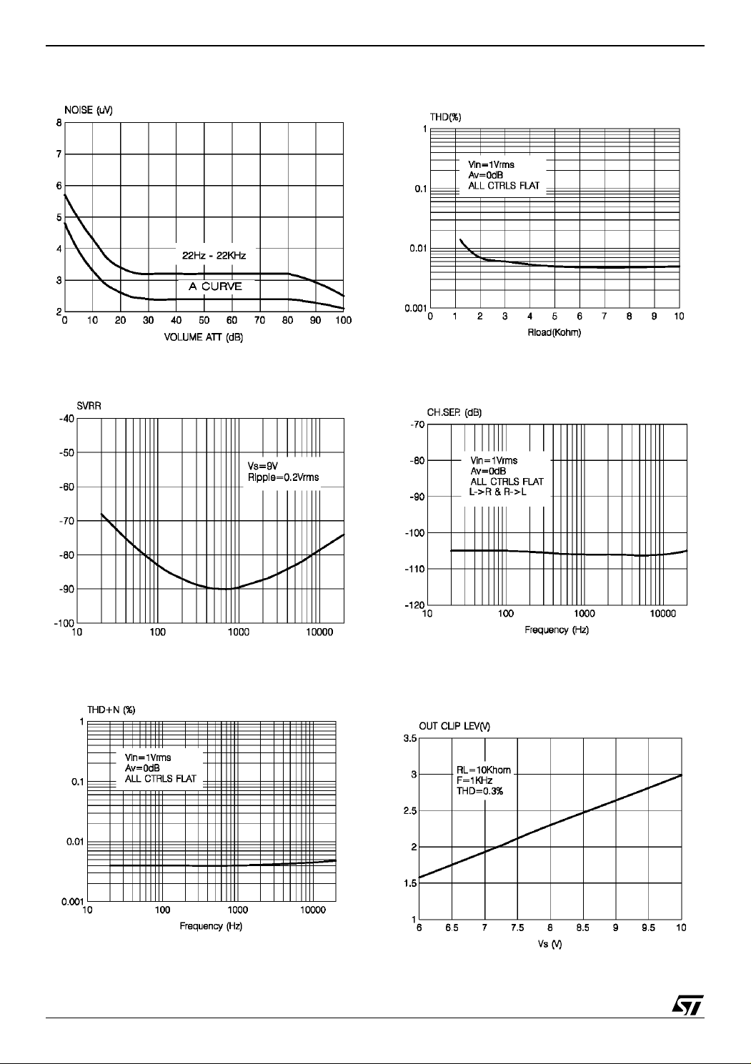
Figure 5. Noise vs. Volume Setting.
Figure 6. SVRR vs. Frequency.
Figure 8. THD vs. R
LOAD
.
Figure 9. Channel Separation vs. Frequency.
Figure 7. THD vs. frequency
4/14
Figure 10. Output Clip Level vs. Supply
Voltage.
TDA7309
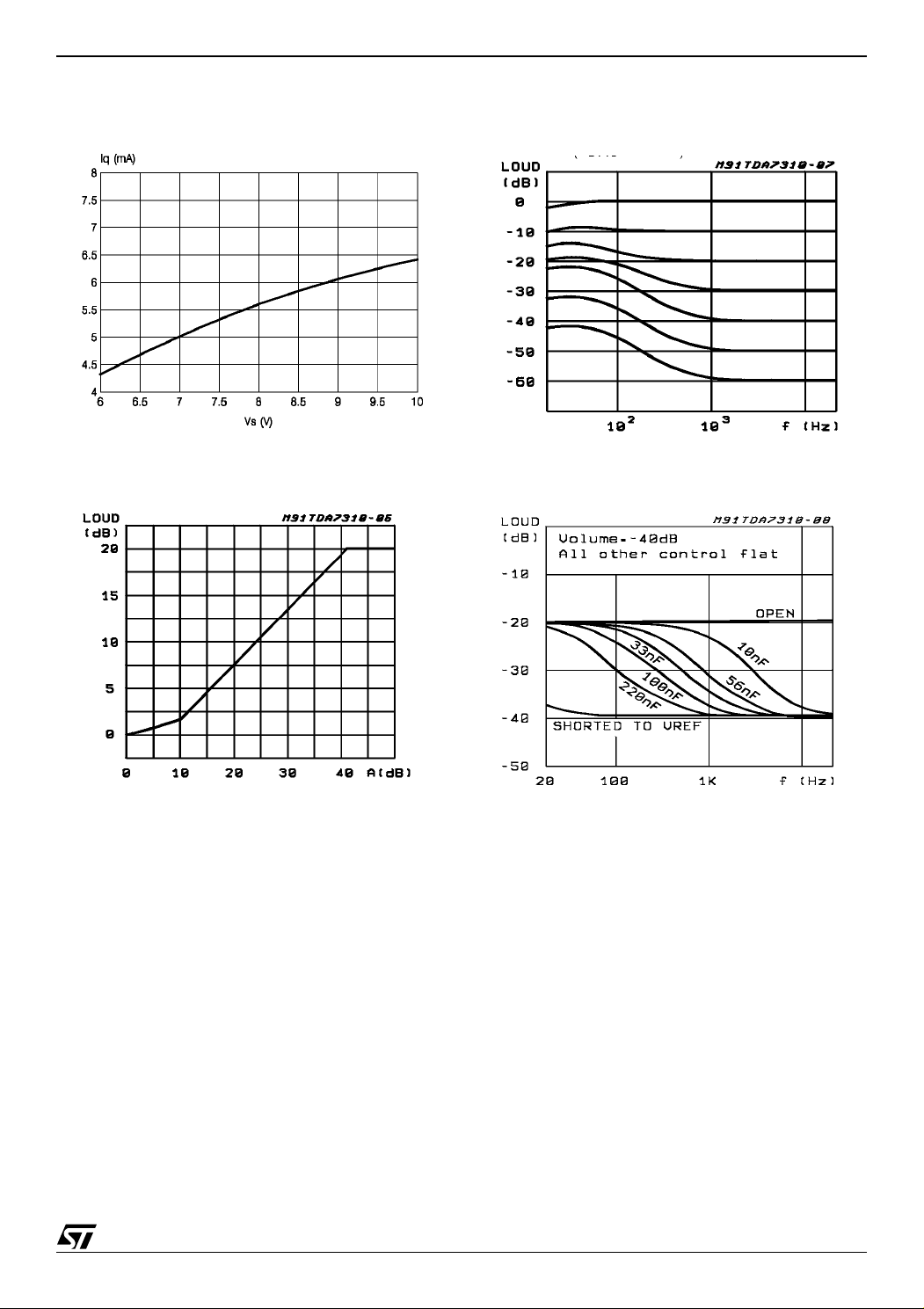
Figure 11. Quiescen Current vs. Supply
Voltage
Figure 12. Loudness vs. Volume Attenuation
Figure 13. Loudness vs. Frequency
(C
= 100nF) vs. Volume
LOAD
Figure 14. Loudness vs. External Capacitors
5/14

TDA7309
3I2C BUS INTERFACE
Data transmission from microprocessor to the TDA7313 and viceversa takes place thru the 2 wires I2C
BUS interface, consisting of the two lines SDA and SCL (pull-up resistors to positive supply voltage must
be connected).
3.1 Data Validity
As shown in fig. 11, the data on the SDA line must be stable during the high period of the clock. The HIGH
and LOW state of the data line can only change when the clock signal on the SCL line is LOW.
3.2 Start and Stop Conditions
As shown in fig. 16 a start condition is a HIGH to LOW transition of the SDA line while SCL is HIGH. The
stop condition is a LOW to HIGH transition of the SDA line while SCL is HIGH.
3.3 Byte Format
Every byte transferred on the SDA line must contain 8 bits. Each byte must be followed by an acknowledge
bit. The MSB is transferred first.
3.4 Acknowledge
The master (µP) puts a resistive HIGH level on the SDA line during the acknowledge clock pulse (see fig.
17). The peripheral (audioprocessor) that acknowledges has to pull-down (LOW) the SDA line during the
acknowledge clock pulse, so that the SDA line is stable LOW during this clock pulse.
The audioprocessor which has been addressed has to generate an acknowledge after the reception of
each byte, otherwise the SDA line remains at the HIGH level during the ninth clock pulse time. In this case
the master transmitter can generate the STOP information in order to abort the transfer.
3.5 Transmission without Acknowledge
Avoiding to detect the acknowledge of the audioprocessor, the µP can use a simplier transmission: simply
it waits one clock without checking the slave acknowledging, and sends the new data. This approach of
course is less protected from misworking and decreases the noise immunity.
2
Figure 15. Data Validity on the I
SDA
SCL
Figure 16. Timing Diagram of I
SCL
SDA
START
CBUS
DATA LINE
STABLE, DATA
VALID
2
CBUS
CHANGE
DATA
ALLOWED
D99AU1032
D99AU1031
STOP
2
CBUS
I
6/14

Figure 17. Acknowledge on the I2CBUS
TDA7309
SCL
SDA
Table 6. SDA, SCL I
START
2
CBUS Timing
1
MSB
23789
D99AU1033
ACKNOWLEDGMENT
FROM RECEIVER
Symbol Parameter Min. Typ. Max. Unit
f
SCL
t
BUF
t
HD:STA
SCL clock frequency 0 400 kHz
Bus free time between a STOP and START condition 1.3 µs
Hold time (repeated) START condition. After this period, the first
0.6 µs
clock pulse is generated
t
LOW
t
HIGH
t
SU:STA
t
HD:DA
t
SU:DAT
LOW period of the SCL clock 1.3 µs
HIGH period of the SCL clock 0.6 µs
Set-up time for a repeated START condition 0.6 µs
Data hold time 0.300 µs
Data set-up time 100 ns
t
R
t
F
t
SU:STO
All values referred to VIH min. and VIL max. levels
(*) Must be guaranteed by the I
Rise time of both SDA and SCL signals 20 300 ns (*)
Fall time of both SDA and SCL signals 20 300 ns (*)
Set-up time for STOP condition 0.6 µs
2
C BUS master.
Figure 18. Definition of Timing on the I2C-bus
SDA
t
SCL
BUF
P S
P = STOP
S = START
t
HD;STA
t
LOW
t
RtF
t
HD;DAT
t
HIGH
t
t
t
HD;STA
t
t
SU;DAT
SU;STA
Sr P
D95AU314
F
SU;STO
t
SP
7/14

TDA7309
4 SOFTWARE SPECIFICATION
4.1 Interface Protocol
The interface protocol comprises:
■ A start condition (s)
■ A chip address byte, containing the TDA7309 address (the 8th bit of the byte must be 0).
The TDA7309 must always acknowledge at the end of each transmitted byte.
■ A sequence of data (N-bytes + acknowledge)
■ A stop condition (P)
Figure 19.
ACK = Acknowledge
S = Start
P = Stop
MAX CLOCK SPEED 400kbits/s
Table 7. Chip address
MSB LSB
00110010pin address open
00110000pin address close to ground
Table 8. Function Codes
MSBF6F5F4F3F2F1LSB
VOLUME 0XXXXXXX
MUTE/LOUD 1 0 0 X X X X X
INPUTS 1 0 1 X X X X X
CHANNEL 1 1 0 X X X X X
Table 9. Channel Abilitation Codec
MSB F6 F5 F4 F3 F2 F1 LSB FUNCTION
1 1 0 channel
XXX0 0RIGHT
XXX0 1LEFT
XXX1 0BOTH
XXX1 1BOTH
8/14

4.2 Power on reset condition
1 1 1 1 1 1 1 0
Table 10. Volume Codes
MSB F6 F5 F4 F3 F2 F1 LSB FUNCTION
0 step 1dB
000 0dB
001 -1dB
010 -2dB
011 -3dB
100 -4dB
101 -5dB
110 -6dB
111 -7dB
0 step 8dB
0000 0dB
0001 -8dB
0010 -16dB
0011 -24dB
0100 -32dB
0101 -40dB
0110 -48dB
0111 -56dB
1000 -64dB
1001 -72dB
1010 -80dB
1011 -88dB
11XX MUTE
TDA7309
Table 11. Mute Loudness Codes
MSB F6 F5 F4 F3 F2 F1 LSB FUNCTION
1 0 0 mute/loud
X 0 0 slow soft mute on
X 0 1 fast soft mute on
1 soft mute off
1 LOUD OFF
X 0 0 loud on (10dB)
X 1 0 loud on (20dB)
9/14

TDA7309
Table 12. Input Multiplexer Codes
MSBF6F5F4F3F2F1LSB FUNCTION
101 inputs
XXX0 0 MUTE
XXX0 1 IN2
XXX1 0 IN3
XXX1 1 IN1
Purchase of I2C Components of STMicrolectronics, conveys a license under the Philips I2C Patent
Rights to use these components in an I
2
C system, provided that the system conforms to the I2C Stan-
dard Specifications as defined by Philips.
10/14

Figure 20. DIP20 Mechanical Data & Package Dimensions
TDA7309
DIM.
a1 0.254 0.010
B 1.39 1.65 0.055 0.065
b 0.45 0.018
b1 0.25 0.010
D 25.4 1.000
E 8.5 0.335
e 2.54 0.100
e3 22.86 0.900
F 7.1 0.280
I 3.93 0.155
L 3.3 0.130
Z 1.34 0.053
mm inch
MIN. TYP. MAX. MIN. TYP. MAX.
OUTLINE AND
MECHANICAL DATA
DIP20
11/14

TDA7309
Figure 21. SO20 Mechanical Data & Package Dimensions
DIM.
A 2.35 2.65 0.093 0.104
A1 0.10 0.30 0.004 0.012
B 0.33 0.51 0.013 0.200
C 0.23 0.32 0.009 0.013
(1)
12.60 13.00 0.496 0.512
D
E 7.40 7.60 0.291 0.299
e 1.27 0.050
H 10.0 10.65 0.394 0.419
h 0.25 0.75 0.010 0.030
L 0.40 1.27 0.016 0.050
k 0˚ (min.), 8˚ (max.)
ddd 0.10 0.004
(1) “D” dimension does not include mold flash, protusions or gate
burrs. Mold flash, protusions or gate burrs shall not exceed
0.15mm per side.
mm inch
MIN. TYP. MAX. MIN. TYP. MAX.
OUTLINE AND
MECHANICAL DATA
SO20
12/14
0016022 D

Table 13. Revision History
Date Revision Description of Changes
January 2004 5 First Issue in EDOCS DMS
March 2006 6 Modified on the page 8/14 the “MAX CLOCK SPEED” to 400kbits/s.
TDA7309
13/14

TDA7309
Please Read Carefully:
Information in this document is provided solely in connection with ST products. STMicroelectronics NV and its subsidiaries (“ST”) reserve the
right to make changes, corrections, modifications or improvements, to this document, and the products and services described herein at any
time, without notice.
All ST products are sold pursuant to ST’s terms and conditions of sale.
Purchasers are solely responsible for the choice, selection and use of the ST products and services described herein, and ST assumes no
liability whatsoever relating to the choice, selection or use of the ST products and services described herein.
No license, express or implied, by estoppel or otherwise, to any intellectual property rights is granted under this document. If any part of this
document refers to any third party products or services it shall not be deemed a license grant by ST for the use of such third party products
or services, or any intellectual property contained therein or considered as a warranty covering the use in any manner whatsoever of such
third party products or services or any intellectual property contained therein.
UNLESS OTHERWISE SET FORTH IN ST’S TERMS AND CONDITIONS OF SALE ST DISCLAIMS ANY EXPRESS OR IMPLIED WARRANTY WITH RESPECT TO THE USE AND/OR SALE OF ST PRODUCTS INCLUDING WITHOUT LIMITATION IMPLIED WARRANTIES
OF MERCHANTABILITY, FITNESS FOR A PARTICULAR PURPOSE (AND THEIR EQUIVALENTS UNDER THE LAWS OF ANY JURISDICTION), OR INFRINGEMENT OF ANY PATENT, COPYRIGHT OR OTHER INTELLECTUAL PROPERTY RIGHT.
UNLESS EXPRESSLY APPROVED IN WRITING BY AN AUTHORIZE REPRESENTATIVE OF ST, ST PRODUCTS ARE NOT DESIGNED,
AUTHORIZED OR WARRANTED FOR USE IN MILITARY, AIR CRAFT, SPACE, LIFE SAVING, OR LIFE SUSTAINING APPLICATIONS,
NOR IN PRODUCTS OR SYSTEMS, WHERE FAILURE OR MALFUNCTION MAY RESULT IN PERSONAL INJURY, DEATH, OR SEVERE PROPERTY OR ENVIRONMENTAL DAMAGE.
Resale of ST products with provisions different from the statements and/or technical features set forth in this document shall immediately void
any warranty granted by ST for the ST product or service described herein and shall not create or extend in any manner whatsoever, any
liability of ST.
ST and the ST logo are trademarks or registered trademarks of ST in various countries.
Information in this document supersedes and replaces all information previously supplied.
The ST logo is a registered trademark of STMicroelectronics. All other names are the property of their respective owners.
© 2006 STMicroelectronics - All rights reserved
Australia - Belgium - Brazil - Canada - China - Czech Republic - Finland - France - Germany - Hong Kong - India - Israel - Italy - Japan -
Malaysia - Malta - Morocco - Singapore - Spain - Sweden - Switzerland - United Kingdom - United States of America
STMicroelectronics group of companies
www.st.com
14/14
 Loading...