

Page 1

Digital controlled stereo audio processor with loudness
Features
■ Input multiplexer:
– 3 stereo inputs
– Selectable input gain for optimal adaptation
to different sources
■ Volume control in 1.25 dB steps
■ Loudness function
■ Treble and bass controL
■ Four speaker attenuators:
– 4 independent speakers control in 1.25d B
steps for balance and fader facilities
– Independent mute function
■ All functions programmable via serial I
2
C bus
TDA7303
SO-28
Selectable input gain and external loudness
function are provided. Control is accomplished by
2
serial I
C bus microprocessor interface.
Description
The TDA7303 is a volume, tone (bass and treble)
balance (left/right) and fader (front/rear)
processor for quality audio applications in car
radio, Hi-Fi and portable systems.
Table 1. Device summary
Order code Package Packing
TDA7303 SO-28 Tray
TDA7303TR SO-28 Tape and reel
The AC signal setting is obtained by resistor
networks and switches combined with operational
amplifiers.
Thanks to the used bipolar/CMOS technology, low
distortion, low noise and low DC stepping are
obtained.
March 2009 Rev 3 1/20
1
Page 2

Contents TDA7303
Contents
1 Block, test and pin diagrams . . . . . . . . . . . . . . . . . . . . . . . . . . . . . . . . . . 5
1.1 Block diagram . . . . . . . . . . . . . . . . . . . . . . . . . . . . . . . . . . . . . . . . . . . . . . . 5
1.2 Test circuit . . . . . . . . . . . . . . . . . . . . . . . . . . . . . . . . . . . . . . . . . . . . . . . . . 6
1.3 Pin connection . . . . . . . . . . . . . . . . . . . . . . . . . . . . . . . . . . . . . . . . . . . . . . 6
2 Electrical specifications . . . . . . . . . . . . . . . . . . . . . . . . . . . . . . . . . . . . . . 7
2.1 Absolute maximum ratings . . . . . . . . . . . . . . . . . . . . . . . . . . . . . . . . . . . . . 7
2.2 Quick reference data . . . . . . . . . . . . . . . . . . . . . . . . . . . . . . . . . . . . . . . . . 7
2.3 Thermal data . . . . . . . . . . . . . . . . . . . . . . . . . . . . . . . . . . . . . . . . . . . . . . . 7
2.4 Electrical characteristics . . . . . . . . . . . . . . . . . . . . . . . . . . . . . . . . . . . . . . . 8
2.5 Electrical characteristics curves . . . . . . . . . . . . . . . . . . . . . . . . . . . . . . . . 10
3I
2
C bus interface . . . . . . . . . . . . . . . . . . . . . . . . . . . . . . . . . . . . . . . . . . . 13
3.1 Data validity . . . . . . . . . . . . . . . . . . . . . . . . . . . . . . . . . . . . . . . . . . . . . . . 13
3.2 Start and stop conditions . . . . . . . . . . . . . . . . . . . . . . . . . . . . . . . . . . . . . 13
3.3 Byte format . . . . . . . . . . . . . . . . . . . . . . . . . . . . . . . . . . . . . . . . . . . . . . . . 13
3.4 Acknowledge . . . . . . . . . . . . . . . . . . . . . . . . . . . . . . . . . . . . . . . . . . . . . . 13
3.5 Transmission without acknowledge . . . . . . . . . . . . . . . . . . . . . . . . . . . . . 13
4 Software specification . . . . . . . . . . . . . . . . . . . . . . . . . . . . . . . . . . . . . . 15
4.1 Interface protocol . . . . . . . . . . . . . . . . . . . . . . . . . . . . . . . . . . . . . . . . . . . 15
4.2 Subaddress (receive mode) . . . . . . . . . . . . . . . . . . . . . . . . . . . . . . . . . . . 15
4.3 Data bytes (detailed description) . . . . . . . . . . . . . . . . . . . . . . . . . . . . . . . 16
5 Package information . . . . . . . . . . . . . . . . . . . . . . . . . . . . . . . . . . . . . . . . 18
6 Revision history . . . . . . . . . . . . . . . . . . . . . . . . . . . . . . . . . . . . . . . . . . . 19
2/20
Page 3

TDA7303 List of tables
List of tables
Table 1. Device summary . . . . . . . . . . . . . . . . . . . . . . . . . . . . . . . . . . . . . . . . . . . . . . . . . . . . . . . . . . 1
Table 2. Absolute maximum ratings . . . . . . . . . . . . . . . . . . . . . . . . . . . . . . . . . . . . . . . . . . . . . . . . . . 7
Table 3. Quick reference data . . . . . . . . . . . . . . . . . . . . . . . . . . . . . . . . . . . . . . . . . . . . . . . . . . . . . . 7
Table 4. Thermal data. . . . . . . . . . . . . . . . . . . . . . . . . . . . . . . . . . . . . . . . . . . . . . . . . . . . . . . . . . . . . 7
Table 5. Electrical characteristics . . . . . . . . . . . . . . . . . . . . . . . . . . . . . . . . . . . . . . . . . . . . . . . . . . . . 8
Table 6. Chip address. . . . . . . . . . . . . . . . . . . . . . . . . . . . . . . . . . . . . . . . . . . . . . . . . . . . . . . . . . . . 15
Table 7. Data bytes. . . . . . . . . . . . . . . . . . . . . . . . . . . . . . . . . . . . . . . . . . . . . . . . . . . . . . . . . . . . . . 15
Table 8. Volume . . . . . . . . . . . . . . . . . . . . . . . . . . . . . . . . . . . . . . . . . . . . . . . . . . . . . . . . . . . . . . . . 16
Table 9. Speaker attenuators . . . . . . . . . . . . . . . . . . . . . . . . . . . . . . . . . . . . . . . . . . . . . . . . . . . . . . 16
Table 10. Audio switch . . . . . . . . . . . . . . . . . . . . . . . . . . . . . . . . . . . . . . . . . . . . . . . . . . . . . . . . . . . . 17
Table 11. Bass and treble . . . . . . . . . . . . . . . . . . . . . . . . . . . . . . . . . . . . . . . . . . . . . . . . . . . . . . . . . . 17
Table 12. Document revision history . . . . . . . . . . . . . . . . . . . . . . . . . . . . . . . . . . . . . . . . . . . . . . . . . 19
3/20
Page 4

List of figures TDA7303
List of figures
Figure 1. Block diagram . . . . . . . . . . . . . . . . . . . . . . . . . . . . . . . . . . . . . . . . . . . . . . . . . . . . . . . . . . . . 5
Figure 2. Test circuit . . . . . . . . . . . . . . . . . . . . . . . . . . . . . . . . . . . . . . . . . . . . . . . . . . . . . . . . . . . . . . 6
Figure 3. Pin connection (top view) . . . . . . . . . . . . . . . . . . . . . . . . . . . . . . . . . . . . . . . . . . . . . . . . . . . 6
Figure 4. Loudness vs. volume attenuation . . . . . . . . . . . . . . . . . . . . . . . . . . . . . . . . . . . . . . . . . . . . 10
Figure 5. Loudness vs. frequency (CLOUD = 100 nF) vs. volume attenuation . . . . . . . . . . . . . . . . . 10
Figure 6. Loudness vs. external capacitors . . . . . . . . . . . . . . . . . . . . . . . . . . . . . . . . . . . . . . . . . . . . 10
Figure 7. Noise vs. volume/gain setting . . . . . . . . . . . . . . . . . . . . . . . . . . . . . . . . . . . . . . . . . . . . . . . 10
Figure 8. Signal to noise ratio vs. volume setting . . . . . . . . . . . . . . . . . . . . . . . . . . . . . . . . . . . . . . . 10
Figure 9. Distortion and noise vs. frequency (V
Figure 10. Distortion and noise vs. frequency (V
Figure 11. Distortion vs. load resistance . . . . . . . . . . . . . . . . . . . . . . . . . . . . . . . . . . . . . . . . . . . . . . . 11
Figure 12. Channel separation (L Æ R) vs. frequency. . . . . . . . . . . . . . . . . . . . . . . . . . . . . . . . . . . . . 11
Figure 13. Input separation (L1 Æ L2, L3) vs. frequency. . . . . . . . . . . . . . . . . . . . . . . . . . . . . . . . . . . 11
Figure 14. Supply voltage rejection vs. frequency . . . . . . . . . . . . . . . . . . . . . . . . . . . . . . . . . . . . . . . . 11
Figure 15. Output clipping level vs. supply voltage . . . . . . . . . . . . . . . . . . . . . . . . . . . . . . . . . . . . . . . 11
Figure 16. Quiescent current vs. supply voltage . . . . . . . . . . . . . . . . . . . . . . . . . . . . . . . . . . . . . . . . . 12
Figure 17. Supply current vs. temperature. . . . . . . . . . . . . . . . . . . . . . . . . . . . . . . . . . . . . . . . . . . . . . 12
Figure 18. Bass resistance vs. temperature . . . . . . . . . . . . . . . . . . . . . . . . . . . . . . . . . . . . . . . . . . . . 12
Figure 19. Typical tone response (with the external components indicated in the test circuit) . . . . . . 12
Figure 20. Data validity on the I
Figure 21. Timing diagram of S-bus and I
Figure 22. Acknowledge on the I
2
C bus . . . . . . . . . . . . . . . . . . . . . . . . . . . . . . . . . . . . . . . . . . . . . . . . 14
2
C bus . . . . . . . . . . . . . . . . . . . . . . . . . . . . . . . . . . . . . . . . . . . . . . . 14
2
C bus. . . . . . . . . . . . . . . . . . . . . . . . . . . . . . . . . . . . . . . . . 14
Figure 23. Interface protocol . . . . . . . . . . . . . . . . . . . . . . . . . . . . . . . . . . . . . . . . . . . . . . . . . . . . . . . . 15
Figure 24. SO-28 mechanical data and package dimensions . . . . . . . . . . . . . . . . . . . . . . . . . . . . . . . 18
= 1 V) . . . . . . . . . . . . . . . . . . . . . . . . . . . . . . . . . . 10
IN
= 250 mV). . . . . . . . . . . . . . . . . . . . . . . . . . . . . . . 11
IN
4/20
Page 5
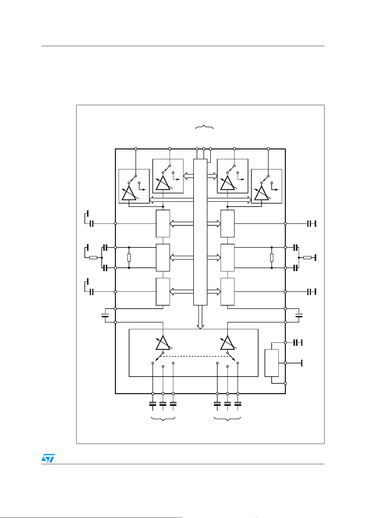
TDA7303 Block, test and pin diagrams
1 Block, test and pin diagrams
1.1 Block diagram
Figure 1. Block diagram
BUS
C17
5.6K R2
C11
2.7nF
100nF
100nF
100nF
TREBLE(L)
C15
BIN(L)
BOUT(L)
C14
LOUD(L)
4
18
19
12
ATT
SPKR
FRONT
OUT LEFT
25
MUTE
RB
ATT
SPKR
VOL
REAR
OUT LEFT
23
TREBLE
BASS
+ LOUD
MUTE
ATT
SPKR
VOL
FRONT
OUT RIGHT
24
BASS TREBLE
+ LOUD
MUTE
SCL
SDA
DIGGND
282726
SERIAL BUS DECODER + LATCHES
ATT
SPKR
REAR
OUT RIGHT
22
MUTE
RB
D98AU888
TREBLE(R)
5
BOUT(R) BIN(R)
21 20
LOUD(R)
8
C13
100nF
C12
100nF
C16
2.7nF
5.6K R1
C10
100nF
OUT(R) IN(R)
CREF
AGND
S
V
C8 2.2μF
22μFC7
C9 2.2μF
17 16
OUT(L) IN(L)
INPUT
+ GAIN
SELECTOR
3x
2.2μF
L1 15L1L2 14L2L3 13
C1
C2
LEFT
INPUTS
L3
R3 9R3R2 10R2R1 11
C3
C4
C5
RIGHT
R1
C6
INPUTS
3x
2.2μF
76
SUPPLY
231
5/20
Page 6
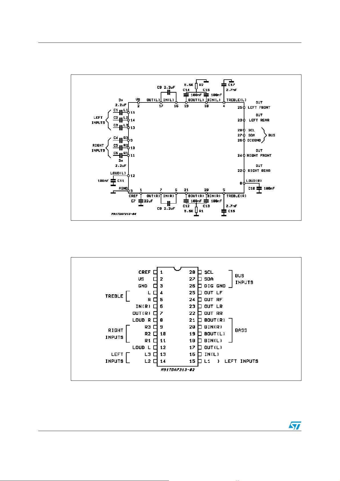
Block, test and pin diagrams TDA7303
1.2 Test circuit
Figure 2. Test circuit
1.3 Pin connection
Figure 3. Pin connection (top view)
6/20
Page 7

TDA7303 Electrical specifications
2 Electrical specifications
2.1 Absolute maximum ratings
Table 2. Absolute maximum ratings
Symbol Parameter Value Unit
T
V
amb
T
Operating supply voltage 10.0 V
S
Ambient temperature -40 to 85 °C
Storage temperature range -55 to +150 °C
stg
2.2 Quick reference data
Table 3. Quick reference data
Symbol Parameter Min. Typ. Max. Unit
V
V
CL
THD Total harmonic distortion V = 1 Vrms; f = 1 kHz 0.01 %
S/N Signal to noise ratio 106 dB
S
Supply voltage 6 9 10 V
S
Max. input signal handling 2 Vrms
Channel separation f = 1 kHz 103 dB
C
Volume control 1.25d B step -78.75 0 dB
Bass and treble control 2 dB step -14 +14 dB
Fader and balance control 1.25 dB step -38.75 0 dB
Input gain 3.75 dB step1.25 dB step 0 11.25 dB
Mute attenuation 100 dB
2.3 Thermal data
Table 4. Thermal data
Symbol Parameter Value Unit
R
th j-pins
Thermal resistance junction to pins Max. 85 °C/W
7/20
Page 8
Electrical specifications TDA7303
2.4 Electrical characteristics
Table 5. Electrical characteristics
(T
= 25 °C, VS = 9 V, RL = 10 kΩ, RG = 600 Ω, all control flat (G = 0), f = 1 kHz unless
amb
otherwise specified)
Symbol Parameter Test condition Min. Typ. Max. Unit
Supply
V
Supply voltage 6 9 10 V
S
Supply current 8 11 mA
I
S
SVR Ripple rejection 60 80 dB
Input selectors
R
Input resistance Input 1, 2, 3, 4 50 kΩ
II
V
S
G
G
INmax
G
Volu m e co n t rol
Clipping level 2 2.5 Vrms
CL
Input separation
IN
Output load resistance pin 7, 17 2 kΩ
R
L
Min. input gain -1 0 1 dB
INmin
(2)
80 100 dB
Max. input gain 11.25 dB
Step resolution 3.75 dB
STEP
e
Input noise G = 11.25 dB 2 µV
IN
R
C
RANGE
A
A
VMAX
A
Input resistance 33 kΩ
IN
Control range 70 75 80 dB
Min. attenuation -1 0 1 dB
VMIN
Max. attenuation 70 75 80 dB
Step resolution 0.5 1.25 1.75 dB
STEP
AV = 0 to -20 dB -1.25 0 1.25 dB
E
Attenuation set error
A
Tracking error 2dB
E
T
= -20 to -60 dB -3 2 dB
A
V
Speaker attenuators
C
S
A
MUTE
Bass control
Control range 35 37.5 40 dB
range
Step resolution 0.5 1.25 1.75 dB
STEP
Attenuation set error 1.5 dB
E
A
Output mute attenuation 80 100 dB
(1)
Gb Control range Max. Boost/cut ±12 ±14 ±16 dB
B
STEP
Step resolution 1 2 3 dB
8/20
Page 9

TDA7303 Electrical specifications
Table 5. Electrical characteristics (continued)
(T
= 25 °C, VS = 9 V, RL = 10 kΩ, RG = 600 Ω, all control flat (G = 0), f = 1 kHz unless
amb
otherwise specified)
Symbol Parameter Test condition Min. Typ. Max. Unit
R
Treble control
Internal feedback resistance 44 kΩ
B
(1)
Gt Control range Max. Boost/cut ±13 ±14 ±15 dB
T
STEP
Step Resolution 1 2 3 dB
Audio outputs
V
R
V
Clipping level d = 0.3 % 2 2.5 Vrms
OCL
R
Output load resistance 2 kΩ
L
Output load capacitance 10 nF
C
L
Output resistance 75 Ω
OUT
DC voltage level 4.2 4.5 4.8 V
OUT
General
BW = 20-20 kHz, flat
e
NO
Output noise
(2)
output muted
all gains = 0 dB
2.5
5
A curve all gains = 0 dB 3 µV
S/N Signal to noise ratio all gains = 0 dB; V
A
= 0; VIN = 1 Vrms 0.01 %
V
d Distortion
= -20 dB, VIN = 1 Vrms 0.09 0.3 %
A
V
= -20 dB, VIN = 0.3 Vrms 0.04 %
A
V
= 1 Vrms 106 dB
O
Sc Channel separation left/right 80 103 dB
A
= 0 to -20 dB 0 1 dB
Total tracking error
V
-20 to -60 dB 0 2 dB
µV
µV
Bus inputs
V
V
V
1. Bass and treble response see attached diagram (Figure 19). The center frequency and quality of the resonance behavior
can be chosen by the external circuitry. A standard first order bass response can be realized by a standard feedback
network
2. The selected input is grounded through the 2.2 µF capacitor.
Input low voltage 1V
IL
Input high voltage 3 V
IH
Input current -5 +5 µA
I
IN
Output voltage SDA acknowledge IO = 1.6 mA 0.4 V
O
9/20
Page 10

Electrical specifications TDA7303
2.5 Electrical characteristics curves
Figure 4. Loudness vs. volume attenuation Figure 5. Loudness vs. frequency (C
LOUD
100 nF) vs. volume attenuation
Figure 6. Loudness vs. external capacitors Figure 7. Noise vs. volume/gain setting
=
Figure 8. Signal to noise ratio vs. volume
setting
10/20
Figure 9. Distortion and noise vs. frequency
(V
= 1 V)
IN
Page 11

TDA7303 Electrical specifications
Figure 10. Distortion and noise vs. frequency
(V
= 250 mV)
IN
Figure 12. Channel separation (L → R) vs.
frequency
Figure 11. Distortion vs. load resistance
Figure 13. Input separation (L1 → L2, L3) vs.
frequency
Figure 14. Supply voltage rejection vs.
frequency
Figure 15. Output clipping level vs. supply
voltage
11/20
Page 12

Electrical specifications TDA7303
Figure 16. Quiescent current vs. supply
Figure 17. Supply current vs. temperature
voltage
Figure 18. Bass resistance vs. temperature Figure 19. Typical tone response (with the
external components indicated in
the test circuit)
12/20
Page 13

TDA7303 I2C bus interface
3 I2C bus interface
Data transmission from microprocessor to the TDA7303 and viceversa takes place through
the 2 wires I
positive supply voltage must be connected).
2
C bus interface, consisting of the two lines SDA and SCL (pull-up resistors to
3.1 Data validity
As shown in Figure 20, the data on the SDA line must be stable during the high period of the
clock. The high and low state of the data line can only change when the clock signal on the
SCL line is lOW.
3.2 Start and stop conditions
As shown in Figure 21 a start condition is a high to low transition of the SDA line while SCL
is high. The stop condition is a low to high transition of the SDA line while SCL is high.
3.3 Byte format
Every byte transferred on the SDA line must contain 8 bits. Each byte must be followed by
an acknowledge bit. The MSB is transferred first.
3.4 Acknowledge
The master (μP) puts a resistive HIGH level on the SDA line during the acknowledge clock
pulse (see Figure 22). The peripheral (audioprocessor) that acknowledges has to pull-down
(low) the SDA line during the acknowledge clock pulse, so that the SDA line is stable low
during this clock pulse.
The audioprocessor which has been addressed has to generate an acknowledge after the
reception of each byte, otherwise the SDA line remains at the high level during the ninth
clock pulse time. In this case the master transmitter can generate the stop information in
order to abort the transfer.
3.5 Transmission without acknowledge
Avoiding to detect the acknowledge of the audioprocessor, the μP can use a simpler
transmission: simply it waits one clock without checking the slave acknowledging, and sends
the new data.
This approach of course is less protected from misreading and decreases the noise
immunity.
13/20
Page 14

I2C bus interface TDA7303
Figure 20. Data validity on the I2C bus
SDA
SCL
DATA LINE
STABLE, DATA
VALID
Figure 21. Timing diagram of S-bus and I
SCL
SDA
CHANGE
DATA
ALLOWED
2
C bus
D99AU1031
2
I
CBUS
START
Figure 22. Acknowledge on the I
SCL
SDA
START
1
MSB
D99AU1032
2
C bus
23789
D99AU1033
STOP
ACKNOWLEDGMENT
FROM RECEIVER
Patent note: Purchase of I2C Components of STMicrolectronics,
conveys a license under the Philips I
use these components in an I
system conforms to the I
defined by Philips.
14/20
2
2
C system, provided that the
2
C Standard Specifications as
C Patent Rights to
Page 15

TDA7303 Software specification
4 Software specification
4.1 Interface protocol
The interface protocol comprises:
● A start condition (s)
● A chip address byte, containing the TDA7303 address (the 8th bit of the byte must be
0).
The TDA7303 must always acknowledge at the end of each transmitted byte.
● A sequence of data (N-bytes + acknowledge)
● A stop condition (P)
Figure 23. Interface protocol
ACK = Acknowledge
S = Start
P = Stop
Max. clock speed 400 kbits/s
4.2 Subaddress (receive mode)
Table 6. Chip address
MSB LSB
10 001000
Table 7. Data bytes
MSB LSB Function
0 0 B2 B1 B0 A2 A1 A0 Volume control
1 1 0 B1 B0 A2 A1 A0 Speaker ATT LR
1 1 1 B1 B0 A2 A1 A0 Speaker ATT RR
1 0 0 B1 B0 A2 A1 A0 Speaker ATT LF
1 0 1 B1 B0 A2 A1 A0 Speaker ATT RF
0 1 0 G1 G0 S2 S1 S0 Audio switch
0 1 1 0 C3 C2 C1 C0 Bass control
0 1 1 1 C3 C2 C1 C0 Treble control
Ax = 1.25dB steps; Bx = 10dB steps; Cx = 2dB steps; Gx = 3.75dB steps
15/20
Page 16

Software specification TDA7303
4.3 Data bytes (detailed description)
Table 8. Volume
MSB LSB Function
0 0 B2 B1 B0 A2 A1 A0 Volume 1.25 dB steps
000 0
001 -1.25
010 -2.5
011 -3.75
100 -5
101 -6.25
110 -7.5
111 -8.75
Volume 10 dB steps
000 0
001 -10
010 -20
011 -30
100 -40
101 -50
110 -60
111 -70
For example a volume of -45 dB is given by: 0 0 1 0 0 1 0 0
Table 9. Speaker attenuators
MSB LSB Function
1 0 0 B1 B0 A2 A1 A0 Speaker LF
1 0 1 B1 B0 A2 A1 A0 Speaker RF
1 1 0 B1 B0 A2 A1 A0 Speaker LR
1 1 1 B1 B0 A2 A1 A0 Speaker RR
000 0
0 0 1 -1.25
010 -2.5
0 1 1 -3.75
100 -5
1 0 1 -6.25
110 -7.5
1 1 1 -8.75
00 0
01 -10
10 -20
11 -30
11111 Mute
For example attenuation of 25 dB on speaker RF is given by: 1 0 1 1 0 1 0 0
16/20
Page 17

TDA7303 Software specification
Table 10. Audio switch
MSB LSB Function
0 1 0 G1G0S2S1S0 Audio Switch
0 0 Stereo 1
0 1 Stereo 2
1 0 Stereo 3
11 Not allowed
0 Loudness ON
1 Loudness OFF
0 0 +11.25 dB
0 1 +7.5 dB
1 0 +3.75d B
1 1 0 dB
For example to select the stereo 2 input with a gain of +7.5dB LOUDNESS ON the 8bit
string is: 0 1 0 0 1 0 0 1
Table 11. Bass and treble
MSB LSB Function
0 1 1 0 C3 C2 C1 C0 Bass
0 1 1 1 C3 C2 C1 C0 Treble
0000 -14
0001 -12
0010 -10
0011 -8
0100 -6
0101 -4
0110 -2
0111 0
1111 0
1110 2
1101 4
1100 6
1011 8
1010 10
1001 12
1000 14
C3 = Sign
For example Bass at -10dB is obtained by the following 8 bit string: 0 1 1 0 0 0 1 0
17/20
Page 18

Package information TDA7303
5 Package information
In order to meet environmental requirements, ST offers these devices in different grades of
ECOPACK
®
packages, depending on their level of environmental compliance. ECOPACK
®
specifications, grade definitions and product status are available at: www.st.com.
ECOPACK
®
is an ST trademark.
Figure 24. SO-28 mechanical data and package dimensions
DIM.
A 2.65 0.104
a1 0.1 0.3 0.004 0.012
b 0.35 0.49 0.014 0.019
b1 0.23 0.32 0.009 0.013
C 0.5 0.020
c1 45° (typ.)
D 17.7 18.1 0.697 0.713
E 10 10.65 0.394 0.419
e 1.27 0.050
e3 16.51 0.65
F 7.4 7.6 0.291 0.299
L 0.4 1.27 0.016 0.050
S8
mm inch
MIN. TYP. MAX. MIN. TYP. MAX.
(max.)
°
OUTLINE AND
MECHANICAL DATA
SO-28
18/20
Page 19
TDA7303 Revision history
6 Revision history
Table 12. Document revision history
Date Revision Changes
04-Aug-2006 1 Initial release.
Updated “distortion” parameter in the Table 5: Electrical
characteristics on the page 9.
13-Mar-2009 2
18-Mar-2009 3
Modified the max. clock speed value in Section 4.1: Interface
protocol on page 15.
Updated Section 5: Package information on page 18.
Modified the test condition of the parameter “distortion” in the
Table 5: Electrical characteristics on the page 9.
19/20
Page 20

TDA7303
Please Read Carefully:
Information in this document is provided solely in connection with ST products. STMicroelectronics NV and its subsidiaries (“ST”) reserve the
right to make changes, corrections, modifications or improvements, to this document, and the products and services described herein at any
time, without notice.
All ST products are sold pursuant to ST’s terms and conditions of sale.
Purchasers are solely responsible for the choice, selection and use of the ST products and services described herein, and ST assumes no
liability whatsoever relating to the choice, selection or use of the ST products and services described herein.
No license, express or implied, by estoppel or otherwise, to any intellectual property rights is granted under this document. If any part of this
document refers to any third party products or services it shall not be deemed a license grant by ST for the use of such third party products
or services, or any intellectual property contained therein or considered as a warranty covering the use in any manner whatsoever of such
third party products or services or any intellectual property contained therein.
UNLESS OTHERWISE SET FORTH IN ST’S TERMS AND CONDITIONS OF SALE ST DISCLAIMS ANY EXPRESS OR IMPLIED
WARRANTY WITH RESPECT TO THE USE AND/OR SALE OF ST PRODUCTS INCLUDING WITHOUT LIMITATION IMPLIED
WARRANTIES OF MERCHANTABILITY, FITNESS FOR A PARTICULAR PURPOSE (AND THEIR EQUIVALENTS UNDER THE LAWS
OF ANY JURISDICTION), OR INFRINGEMENT OF ANY PATENT, COPYRIGHT OR OTHER INTELLECTUAL PROPERTY RIGHT.
UNLESS EXPRESSLY APPROVED IN WRITING BY AN AUTHORIZED ST REPRESENTATIVE, ST PRODUCTS ARE NOT
RECOMMENDED, AUTHORIZED OR WARRANTED FOR USE IN MILITARY, AIR CRAFT, SPACE, LIFE SAVING, OR LIFE SUSTAINING
APPLICATIONS, NOR IN PRODUCTS OR SYSTEMS WHERE FAILURE OR MALFUNCTION MAY RESULT IN PERSONAL INJURY,
DEATH, OR SEVERE PROPERTY OR ENVIRONMENTAL DAMAGE. ST PRODUCTS WHICH ARE NOT SPECIFIED AS "AUTOMOTIVE
GRADE" MAY ONLY BE USED IN AUTOMOTIVE APPLICATIONS AT USER’S OWN RISK.
Resale of ST products with provisions different from the statements and/or technical features set forth in this document shall immediately void
any warranty granted by ST for the ST product or service described herein and shall not create or extend in any manner whatsoever, any
liability of ST.
ST and the ST logo are trademarks or registered trademarks of ST in various countries.
Information in this document supersedes and replaces all information previously supplied.
The ST logo is a registered trademark of STMicroelectronics. All other names are the property of their respective owners.
© 2009 STMicroelectronics - All rights reserved
STMicroelectronics group of companies
Australia - Belgium - Brazil - Canada - China - Czech Republic - Finland - France - Germany - Hong Kong - India - Israel - Italy - Japan -
Malaysia - Malta - Morocco - Singapore - Spain - Sweden - Switzerland - United Kingdom - United States of America
www.st.com
20/20
 Loading...