

Page 1

18-bit enhanced port expander with keypad controller
Features
■ 18 GPIOs configurable as GPI, GPO, keypad
matrix, special key or dedicated key function
■ Operating voltage: 1.65 - 3.6 V
■ Hardware keypad controller (KPC)
(10 x 8 matrix with 4 optional dedicated keys
maximum)
■ Keypad controller capable of detecting
keypress in hibernation mode
■ Interrupt output (open drain) pin
■ Advanced power management system
■ Ultra-low standby mode current
■ Programmable pull-up resistors for all GPIO
pins
■ ESD performance on GPIO pins:
– ± 8 kV human body model
(JESD22 A114-C)
■ ESD performance on V
SCL, SDA pins:
– ± 3 kV human body model
(JESD22 A114-C)
, GND, INTB, R
CC
STB
STMPE1801
Xpander Logic™
Flip-chip CSP 25
(2.03 x 2.03 mm)
Description
The STMPE1801 is a GPIO (general purpose
input/output) port expander capable of interfacing
a main digital ASIC via the two-line bidirectional
2
bus (I
,
C). A separate GPIO expander IC is often
used in mobile multimedia platforms to resolve
the problem of the limited number of GPIOs
typically available on digital engines.
The STMPE1801 offers high flexibility, as each
I/O can be configured as input, output, special
key, keypad matrix or dedicated key function. This
device is designed to include very low quiescent
current, and a wakeup feature for each I/O, to
optimize the power consumption of the device.
Potential applications for the STMPE1801 include
portable media players, game consoles, mobile
and smart phones.
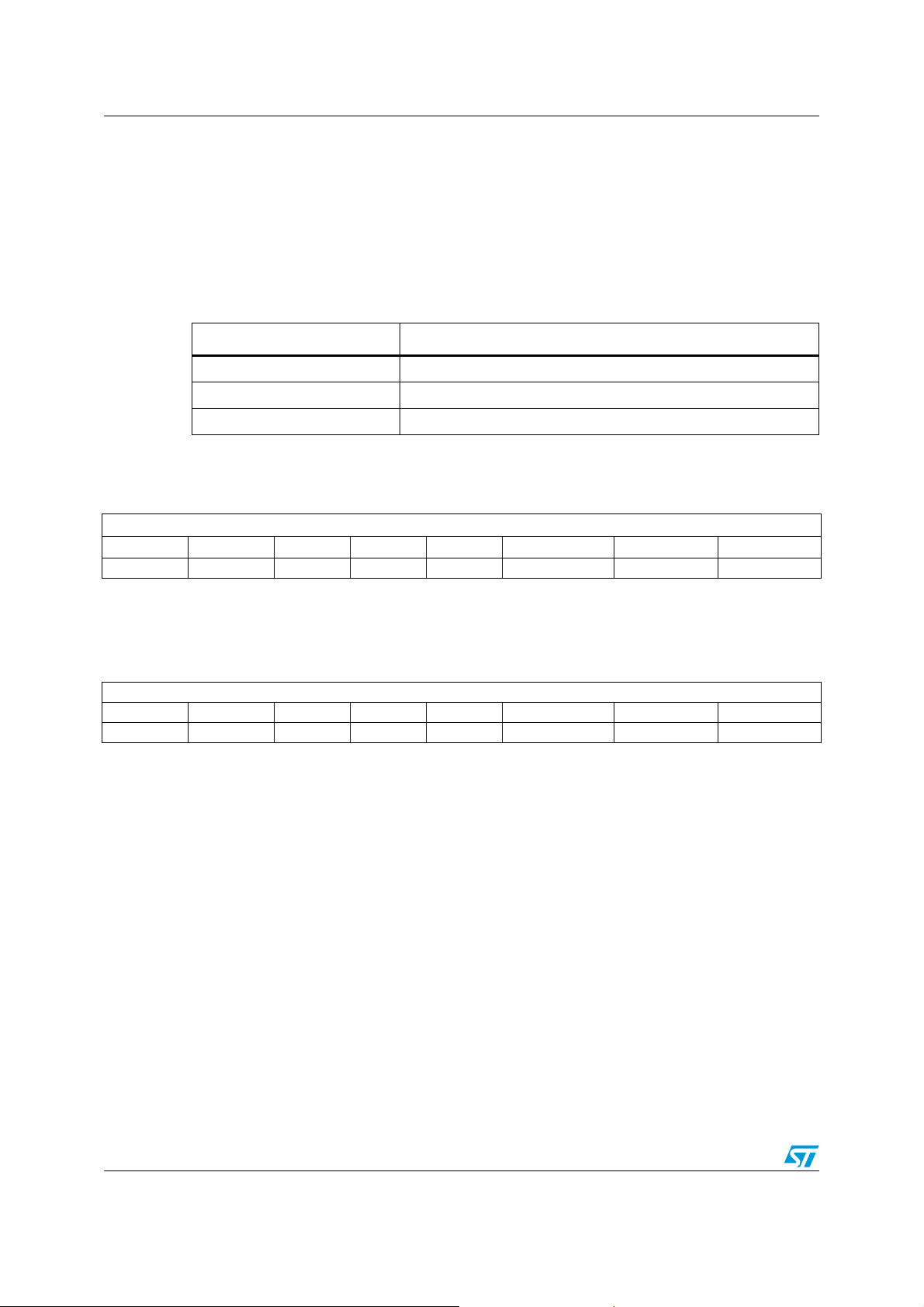
Table 1. Device summary
Order code Package Packaging
STMPE1801BJR
March 2011 Doc ID 17884 Rev 3 1/60
Flip-chip CSP 25 (2.03 x 2.03 mm)
0.4 mm pitch
Tape and reel
www.st.com
60
Page 2

Contents STMPE1801
Contents
1 Block diagram . . . . . . . . . . . . . . . . . . . . . . . . . . . . . . . . . . . . . . . . . . . . . . 4
2 Pin settings . . . . . . . . . . . . . . . . . . . . . . . . . . . . . . . . . . . . . . . . . . . . . . . . 5
2.1 Pin connection . . . . . . . . . . . . . . . . . . . . . . . . . . . . . . . . . . . . . . . . . . . . . . 5
2.2 Pin description . . . . . . . . . . . . . . . . . . . . . . . . . . . . . . . . . . . . . . . . . . . . . . 5
2.3 GPIO pin functions . . . . . . . . . . . . . . . . . . . . . . . . . . . . . . . . . . . . . . . . . . . 6
3 Maximum ratings . . . . . . . . . . . . . . . . . . . . . . . . . . . . . . . . . . . . . . . . . . . . 8
3.1 Absolute maximum ratings . . . . . . . . . . . . . . . . . . . . . . . . . . . . . . . . . . . . . 8
3.2 Thermal data . . . . . . . . . . . . . . . . . . . . . . . . . . . . . . . . . . . . . . . . . . . . . . . 8
4 Electrical specification . . . . . . . . . . . . . . . . . . . . . . . . . . . . . . . . . . . . . . . 9
4.1 DC electrical characteristics . . . . . . . . . . . . . . . . . . . . . . . . . . . . . . . . . . . . 9
4.2 Input/Output DC electrical characteristics . . . . . . . . . . . . . . . . . . . . . . . . 10
5 Register address . . . . . . . . . . . . . . . . . . . . . . . . . . . . . . . . . . . . . . . . . . . 11
6 I2C specification . . . . . . . . . . . . . . . . . . . . . . . . . . . . . . . . . . . . . . . . . . . 14
6.1 I2C related pins . . . . . . . . . . . . . . . . . . . . . . . . . . . . . . . . . . . . . . . . . . . . 14
6.2 I2C addressing . . . . . . . . . . . . . . . . . . . . . . . . . . . . . . . . . . . . . . . . . . . . . 14
6.3 Start condition . . . . . . . . . . . . . . . . . . . . . . . . . . . . . . . . . . . . . . . . . . . . . 14
6.4 Stop condition . . . . . . . . . . . . . . . . . . . . . . . . . . . . . . . . . . . . . . . . . . . . . 14
6.5 Acknowledge bit (ACK) . . . . . . . . . . . . . . . . . . . . . . . . . . . . . . . . . . . . . . . 15
6.6 Data input . . . . . . . . . . . . . . . . . . . . . . . . . . . . . . . . . . . . . . . . . . . . . . . . . 15
6.7 Memory addressing . . . . . . . . . . . . . . . . . . . . . . . . . . . . . . . . . . . . . . . . . 15
6.8 Operation modes . . . . . . . . . . . . . . . . . . . . . . . . . . . . . . . . . . . . . . . . . . . 15
6.9 General call address . . . . . . . . . . . . . . . . . . . . . . . . . . . . . . . . . . . . . . . . 17
7 System controller . . . . . . . . . . . . . . . . . . . . . . . . . . . . . . . . . . . . . . . . . . 18
7.1 System level registers . . . . . . . . . . . . . . . . . . . . . . . . . . . . . . . . . . . . . . . 18
7.2 States of operation . . . . . . . . . . . . . . . . . . . . . . . . . . . . . . . . . . . . . . . . . . 20
7.2.1 . . . . . . . . . . . . . . . . . . . . . . . . . . . . . . . . . . . . . . . . . . . . Auto-hibernate 20
7.2.2 . . . . . . . . . . . . . . . . . . . . . . . . Keypress detect in the Hibernate mode 21
2/60 Doc ID 17884 Rev 3
Page 3

STMPE1801 Contents
8 . . . . . . . . . . . . . . . . . . . . . . . . . . . . . . . . . . . . . . . . . . . Clocking system 22
8.0.1 Clock source . . . . . . . . . . . . . . . . . . . . . . . . . . . . . . . . . . . . . . . . . . . . . 22
8.0.2 Power mode programming sequence . . . . . . . . . . . . . . . . . . . . . . . . . . 23
9 Interrupt system . . . . . . . . . . . . . . . . . . . . . . . . . . . . . . . . . . . . . . . . . . . 24
9.1 Interrupt system register map . . . . . . . . . . . . . . . . . . . . . . . . . . . . . . . . . 25
9.2 Interrupt latency for the GPIO hot keys . . . . . . . . . . . . . . . . . . . . . . . . . . 25
9.3 Programming sequence . . . . . . . . . . . . . . . . . . . . . . . . . . . . . . . . . . . . . . 31
10 GPIO controller . . . . . . . . . . . . . . . . . . . . . . . . . . . . . . . . . . . . . . . . . . . . 32
10.1 GPIO control registers . . . . . . . . . . . . . . . . . . . . . . . . . . . . . . . . . . . . . . . 33
10.1.1 Bit description . . . . . . . . . . . . . . . . . . . . . . . . . . . . . . . . . . . . . . . . . . . . 33
10.2 Hotkey feature . . . . . . . . . . . . . . . . . . . . . . . . . . . . . . . . . . . . . . . . . . . . . 34
10.2.1 Programming sequence for Hotkey . . . . . . . . . . . . . . . . . . . . . . . . . . . . 34
10.2.2 Minimum pulse width . . . . . . . . . . . . . . . . . . . . . . . . . . . . . . . . . . . . . . . 34
11 Keypad controller . . . . . . . . . . . . . . . . . . . . . . . . . . . . . . . . . . . . . . . . . . 35
11.1 Keypad configurations . . . . . . . . . . . . . . . . . . . . . . . . . . . . . . . . . . . . . . . 38
11.2 Keypad controller registers . . . . . . . . . . . . . . . . . . . . . . . . . . . . . . . . . . . . 40
11.3 Data registers . . . . . . . . . . . . . . . . . . . . . . . . . . . . . . . . . . . . . . . . . . . . . . 46
11.4 Keypad combination key registers . . . . . . . . . . . . . . . . . . . . . . . . . . . . . . 50
11.5 Using the keypad controller . . . . . . . . . . . . . . . . . . . . . . . . . . . . . . . . . . . 51
11.5.1 Ghost key handling . . . . . . . . . . . . . . . . . . . . . . . . . . . . . . . . . . . . . . . . 51
11.5.2 Key detection priority . . . . . . . . . . . . . . . . . . . . . . . . . . . . . . . . . . . . . . . 51
11.5.3 Keypad wakeup from Hibernate mode . . . . . . . . . . . . . . . . . . . . . . . . . . 52
11.5.4 Keypad controller combination key interrupt . . . . . . . . . . . . . . . . . . . . . 52
12 Miscellaneous features . . . . . . . . . . . . . . . . . . . . . . . . . . . . . . . . . . . . . . 53
12.1 Reset . . . . . . . . . . . . . . . . . . . . . . . . . . . . . . . . . . . . . . . . . . . . . . . . . . . . 53
13 Package mechanical data . . . . . . . . . . . . . . . . . . . . . . . . . . . . . . . . . . . . 54
14 Revision history . . . . . . . . . . . . . . . . . . . . . . . . . . . . . . . . . . . . . . . . . . . 59
Doc ID 17884 Rev 3 3/60
Page 4

Block diagram STMPE1801
1 Block diagram
Figure 1. STMPE1801 block diagram
'.$
234"
).4"
3#,
3$!
+EYPADCONTROLLER
-AIN&307-
'0)/CONTROL
)#
)NTERFACE
0/2
-58
-58
+EYPADINPUT
2/72/7
'0)/
+EYPADOUTPUT
#/,#/,
'0)/
6
##
4/60 Doc ID 17884 Rev 3
Page 5
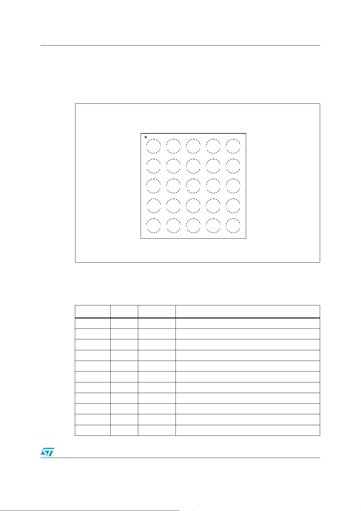
STMPE1801 Pin settings
_
2 Pin settings
2.1 Pin connection
Figure 2. Pin connection (top-through view)
GPIO_14 GPIO9 GPIO2 GPIO7
!
"
RSTB
VCC
GPIO15 GPIO10 NC GPIO6
#
$
%
2.2 Pin description
Table 2. Pin description
Pin number Type Symbol Name and function
D4 I/O GPIO0 GPIO0/ROW0
C4 I/O GPIO1 GPIO1/ROW1
A4 I/O GPIO2 GPIO2/ROW2
E5 I/O GPIO3 GPIO3/ROW3
SDA GPIO16 GPIO1
GPIO17 GPIO0 GPIO4
SCL
INTB GND GPIO13 GPIO8 GPIO3
GPIO11
GPIO12
GPIO5
Flip-chip CSP 25
!-6
D5 I/O GPIO4 GPIO4/ROW4
C5 I/O GPIO5 GPIO5/ROW5
B5 I/O GPIO6 GPIO6/ROW6
A5 I/O GPIO7 GPIO7/ROW7
E4 I/O GPIO8 GPIO8/COL0
A3 I/O GPIO9 GPIO9/COL1
B3 I/O GPIO10 GPIO10/COL2
Doc ID 17884 Rev 3 5/60
Page 6

Pin settings STMPE1801
Table 2. Pin description (continued)
Pin number Type Symbol Name and function
C3 I/O GPIO11 GPIO11/COL3
D3 I/O GPIO12 GPIO12/COL4
E3 I/O GPIO13 GPIO13/COL5
A2 I/O GPIO14 GPIO14/COL6
B2 I/O GPIO15 GPIO15/COL7
C2 I/O GPIO16 GPIO16/COL8
D2 I/O GPIO17 GPIO17/COL9
Open drain interrupt output pin. Programmable active low
E1 O INTB
A1 I RSTB
C1 A SDA I
D1 A SCL I2C clock. Fail safe
(a pull-up resistor is required) or active high (a pull-down
resistor is required). Fail safe. Pull to V
if not in use.
CC
External reset input. Active low. Fail safe. Reset pulse
width must be more than 500 µs to be valid.
2
C data. Fail safe
B4 - NC No connect
B1 - V
E2 - GND Ground
2.3 GPIO pin functions
Table 3. GPIO pin function
Name Primary function Alternate function
GPIO0 GPIO Keypad row 0
GPIO1 GPIO Keypad row 1
GPIO2 GPIO Keypad row 2
GPIO3 GPIO Keypad row 3
GPIO4 GPIO Keypad row 4
GPIO5 GPIO Keypad row 5
GPIO6 GPIO Keypad row 6
GPIO7 GPIO Keypad row 7
GPIO8 GPIO Keypad column 0
GPIO9 GPIO Keypad column 1
CC
Power supply
GPIO10 GPIO Keypad column 2
GPIO11 GPIO Keypad column 3
GPIO12 GPIO Keypad column 4
6/60 Doc ID 17884 Rev 3
Page 7

STMPE1801 Pin settings
Table 3. GPIO pin function
Name Primary function Alternate function
GPIO13 GPIO Keypad column 5
GPIO14 GPIO Keypad column 6
GPIO15 GPIO Keypad column 7
GPIO16 GPIO Keypad column 8
GPIO17 GPIO Keypad column 9
The default function is always GPIO. As soon as the key scanning is enabled through the
keypad registers, the function is then switched to the key function and then any configuration
made in the GPIO registers is ignored.
Doc ID 17884 Rev 3 7/60
Page 8
Maximum ratings STMPE1801
3 Maximum ratings
Stressing the device above the rating listed in the “absolute maximum ratings” table may
cause permanent damage to the device. These are stress ratings only and operation of the
device at these or any other conditions above those indicated in the operating sections of
this specification is not implied. Exposure to absolute maximum rating conditions for
extended periods may affect device reliability.
3.1 Absolute maximum ratings
Table 4. Absolute maximum ratings
Symbol Parameter Value Unit
V
CC
Input voltage on GPIO pin 4.5 V
V
IN
V
ESD
V
ESD
Supply voltage 4.5 V
Minimum ESD protection on each GPIO
pin (HBM model - JESD22 A114-C)
ESD protection on other pins (HBM model -
JESD22 A114-C)
3.2 Thermal data
Table 5. Thermal data
Symbol Parameter Min Typ Max Unit
R
thJA
T
A
T
J
Thermal resistance junction-ambient – 100 – °C/W
Operating ambient temperature -40 25 85 °C
Operating junction temperature -40 25 125 °C
±8 kV
±3 kV
8/60 Doc ID 17884 Rev 3
Page 9
STMPE1801 Electrical specification
4 Electrical specification
4.1 DC electrical characteristics
Table 6. DC electrical characteristics
Val ue
Symbol Parameter Test conditions
Min Typ Max
Unit
V
CC
I
CC
I
HIBERNATE
I
NTB
Supply voltage - 1.65
Active current (core
and analog) - 1 key
press
Hibernate current
Open drain output
current
V
OL(max)
V
CC
V
OL(max)
VCC=3.3 V
1.8 V − 28 55 µA
3.3 V
25 °C
1.8 V
85 °C
25 °C
3.3 V
85 °C
=0.45 V at
=1.8 V
=0.83 V at
− 90 140 µA
−−0.5
−−1
−−0.5
−−1
− 4 − mA
−
3.6 V
µA
µA
Doc ID 17884 Rev 3 9/60
Page 10
Electrical specification STMPE1801
4.2 Input/Output DC electrical characteristics
Table 7. I/O DC electrical characteristics
Val ue
Symbol Parameter Test conditions
V
= 1.8 V −−0.2 V
V
Low level input voltage
IL
CC
= 3.3 V −−0.2 V
V
CC
VCC = 1.8 V 0.8 V
V
V
HYST
V
OL
V
OH
High level input voltage
IH
Schmitt trigger hysteresis
Low level output voltage
High level output voltage
= 3.3 V 0.8 V
V
CC
V
= 1.8 V − 0.10 −
CC
V
= 3.3 V − 0.20 −
CC
I
= 4 mA,
OL
= 1.8 V
V
CC
= 4 mA,
I
OL
= 3.3 V
V
CC
I
= -4 mA,
OH
= 1.8 V
V
CC
= -4 mA,
I
OH
= 3.3 V
V
CC
= 3.3 V.
V
CC
Active
implementation,
R value is
determined by the
R
Equivalent pull-up
UP
resistance
current measured
at 0 V
= 1.8 V. Active
V
CC
implementation,
R value is
determined by the
current measured
at 0 V
Min Typ Max
CC
CC
−−
−−
−−0.45
−−0.45
1.35
2.48
30 60 90
50 100 150
−−
−−
CC
CC
Unit
V
V
V
V
V
kΩ
10/60 Doc ID 17884 Rev 3
Page 11
STMPE1801 Register address
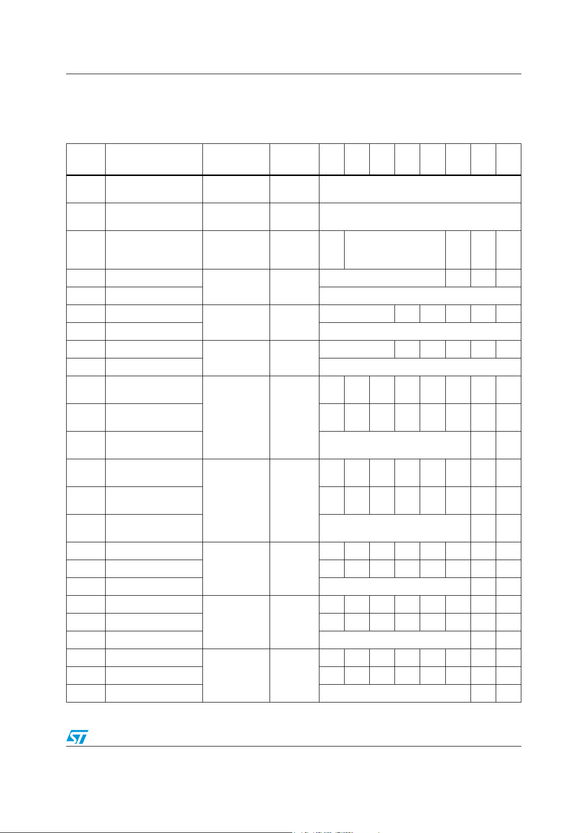
5 Register address
Table 8. STMPE1801 register summary table
Addres
s
00 CHIP_ID
01 VERSION_ID
02 SYS_CTRL System control No
04 INT_CTRL_LOW
05 INT_CTRL_HIGH RESERVED
06 INT_EN_MASK_LOW
07 INT_EN_MASK_HIGH RESERVED
08 INT_STA_LOW
09 INT_STA_HIGH RESERVED
0A
0B
0C
0D INT_STA_GPIO_LOW
0E INT_STA_GPIO_MID
Register name Description
identification
Version
identification
Interrupt
control
Interrupt
enable mask
Interrupt status Yes
INT_EN_GPIO_MASK
_LOW
INT_EN_GPIO_MASK
_MID
INT_EN_GPIO_MASK
_HIGH
Interrupt
enable GPIO
Interrupt status
Chip
mask
GPIO
Auto-
increment
No 8-bit CHIP ID
No 8-bit VERSION ID
Ye s
Ye s
Ye s
Ye s
76543210
SF_
RST
RESERVED IE4 IE3 IE2 IE1 IE0
RESERVED IE4 IE3 IE2 IE1 IE0
IEG7IEG6IEG5IEG4IEG3IEG2IEG1IEG
IEG15IEG14IEG13IEG12IEG11IEG10IEG9IEG
ISG7ISG6ISG
ISG15ISG14ISG13ISG12ISG11ISG10ISG9ISG
RESERVED
RESERVED IC2 IC1 IC0
RESERVED
ISG4ISG3ISG2ISG1ISG
5
GPI
_DB
1
GPI
RSV
_DB
IEG17IEG
D
0
0
8
16
0
8
0F INT_STA_GPIO_HIGH RESERVED
10 GPIO_SET_LOW
11 GPIO_SET_MID IO15 IO14 IO13 IO12 IO11 IO10 IO9 IO8
12 GPIO_SET_HIGH RESERVED IO17 IO16
13 GPIO_CLR_LOW
14 GPIO_CLR_MID IO15 IO14 IO13 IO12 IO11 IO10 IO9 IO8
15 GPIO_CLR_HIGH RESERVED IO17 IO16
16 GPIO_MP_LOW
17 GPIO_MP_MID IO15 IO14 IO13 IO12 IO11 IO10 IO9 IO8
18 GPIO_MP_HIGH RESERVED IO17 IO16
GPIO set pin
state
GPIO clear pin
state
GPIO monitor
pin state
Doc ID 17884 Rev 3 11/60
Ye s
Ye s
Ye s
IO7 IO6 IO5 IO4 IO3 IO2 IO1 IO0
IO7 IO6 IO5 IO4 IO3 IO2 IO1 IO0
IO7 IO6 IO5 IO4 IO3 IO2 IO1 IO0
ISG17ISG
16
Page 12

Register address STMPE1801
Table 8. STMPE1801 register summary table
Addres
s
19 GPIO_SET_DIR_LOW
1A GPIO_SET_DIR_MID IO15 IO14 IO13 IO12 IO11 IO10 IO9 IO8
1B
1C GPIO_RE_LOW
1D GPIO_RE_MID IO15 IO14 IO13 IO12 IO11 IO10 IO9 IO8
1E GPIO_RE_HIGH RESERVED IO17 IO16
1F GPIO_FE_LOW
20 GPIO_FE_MID IO15 IO14 IO13 IO12 IO11 IO10 IO9 IO8
21 GPIO_FE_HIGH RESERVED IO17 IO16
22
23 GPIO_PULL_UP_MID IO15 IO14 IO13 IO12 IO11 IO10 IO9 IO8
24
30 KPC_ROW
Register name Description
GPIO set pin
direction
GPIO_SET_DIR_HIG
H
GPIO_PULL_UP_LO
W
GPIO_PULL_UP_HIG
H
register
GPIO rising
edge
GPIO falling
edge
GPIO pull up Yes
Keypad row
scanning
Auto-
increment
Ye s
Ye s
Ye s
Ye s
76543210
IO7 IO6 IO5 IO4 IO3 IO2 IO1 IO0
RESERVED IO17 IO16
IO7 IO6 IO5 IO4 IO3 IO2 IO1 IO0
IO7 IO6 IO5 IO4 IO3 IO2 IO1 IO0
IO7 IO6 IO5 IO4 IO3 IO2 IO1 IO0
RESERVED IO17 IO16
ROW7ROW6ROW5ROW4ROW3ROW2ROW1RO
W0
31 KPC_COL_LOW
32 KPC_COL_HIGH RESERVED
33 KPC_CTRL_LOW
34 KPC_CTRL_MID DB6 DB5 DB4 DB3 DB2 DB1 DB0
35 KPC_CTRL_HIGH
36 KPC_CMD
37 KPC_COMB_KEY_0
38 KPC_COMB_KEY_1 C4 C3 C2 C1 C0 R2 R1 R0
39 KPC_COMB_KEY_2 C4 C3 C2 C1 C0 R2 R1 R0
Keypad column
scanning
Key config:
Scan count and
dedicated key
Keypad
command
Keypad
combination
key mask
Ye s
Ye s
Yes RESERVED
Ye s
COL7COL6COL5COL4COL3COL2COL1COL
0
COL9COL
8
SCAN_COUNT 0-3 DKEY 0-3
Rsv
d
CM
Rsv
B_K
d
EY
C4 C3 C2 C1 C0 R2 R1 R0
RESERVED
SCAN_FR
EQ
KPC
SCA
_LC
N
K
12/60 Doc ID 17884 Rev 3
Page 13
STMPE1801 Register address
Table 8. STMPE1801 register summary table
Addres
s
Register name Description
Auto-
increment
76543210
UP/
3A KPC_DATA_BYTE0
DWNC3 C2 C1 C0 R2 R1 R0
UP/
3B KPC_DATA_BYTE1
DWNC3 C2 C1 C0 R2 R1 R0
Keypad data Yes
UP/
3C KPC_DATA_BYTE2
DWNC3 C2 C1 C0 R2 R1 R0
3D KPC_DATA_BYTE3 SF7 SF6 SF5 SF4 SF3 SF2 SF1 SF0
3E KPC_DATA_BYTE4 RESERVED Dedicated Key 0 - 3
Doc ID 17884 Rev 3 13/60
Page 14

I2C specification STMPE1801
6 I2C specification
The features supported by the I2C interface are listed below:
2
● I
C slave device
● Operates at V
● Compliant to Philips I
● Supports standard (up to 100 kbps) and fast (up to 400 kbps) modes
● 7-bit device addressing modes
● General call
● Start/Restart/Stop
6.1 I2C related pins
● SCL
● SDA
The device supports both 1.8 V I
Vpullup at SCL and SDA externally is greater or equal to V
(1.8 - 3.6 V)
CC
2
C specification version 2.1
2
C and 3.3 V I2C operations. It is recommended that
.
CC
6.2 I2C addressing
The STMPE1801 7-bit addressing is set to 40h.
6.3 Start condition
A Start condition is identified by a falling edge of SDA while SCL is stable at high state. A
Start condition must precede any data/command transfer. The device continuously monitors
for a Start condition and does not respond to any transaction unless one is encountered.
The first byte is scanned after the START command is detected to check for device ID.
Ensure that all state machines are flushed when START instruction is issued.
6.4 Stop condition
A Stop condition is identified by a rising edge of SDA while SCL is stable at high state. A
Stop condition terminates the communication between the slave device and bus master. A
read command that is followed by NoAck can be followed by a Stop condition to force the
slave device into idle mode. When the slave device is in idle mode, it is ready to receive the
2
next I
C transaction. A Stop condition at the end of a write command stops the write
operation to the registers.
Once the Stop condition is detected, the device should release the bus and go to Hibernate
mode if there is no more activity.
2
An I
C transaction with a START bit followed immediately by a STOP condition should not
cause any I
2
C lock-up.
14/60 Doc ID 17884 Rev 3
Page 15

STMPE1801 I2C specification
6.5 Acknowledge bit (ACK)
The acknowledge bit is used to indicate a successful byte transfer. The bus transmitter
releases the SDA after sending eight bits of data. During the ninth bit, the receiver pulls the
SDA low to acknowledge the receipt of the eight bits of data. The receiver may leave the
SDA in high state if it does not acknowledge the receipt of the data.
6.6 Data input
The device samples the data input on SDA on the rising edge of the SCL. The SDA signal
must be stable during the rising edge of SCL and the SDA signal must change only when
SCL is driven low.
6.7 Memory addressing
For the bus master to communicate to the slave device, the bus master must initiate a Start
condition and be followed by the slave device address. Accompanying the slave device
address, there is a Read/Write bit (R/W
operation.
If a match occurs on the slave device address, the corresponding device gives an
acknowledgement on the SDA during the 9th bit time. If there is no match, it deselects itself
from the bus by not responding to the transaction.
). The bit is set to 1 for Read and 0 for Write
6.8 Operation modes
Table 9. Operating modes
Mode Byte Programming sequence
Read ≥1
START, Device address, R/W
=0, Register Address to be read
RESTART, Device Address, R/W
=1, Data Read, STOP
If no STOP is issued, the Data Read can be continuously performed. If
the register address falls within the range that allows address autoincrement, then register address auto-increments internally after every
byte of data being read. For register address that fails within a nonincremental address range, the address is kept static throughout the
entire read operation. Refer to Table 8.: STMPE1801 register summary
table for the address ranges that are auto-increment and non-increment.
An example of such a non-increment address is FIFO.
Doc ID 17884 Rev 3 15/60
Page 16
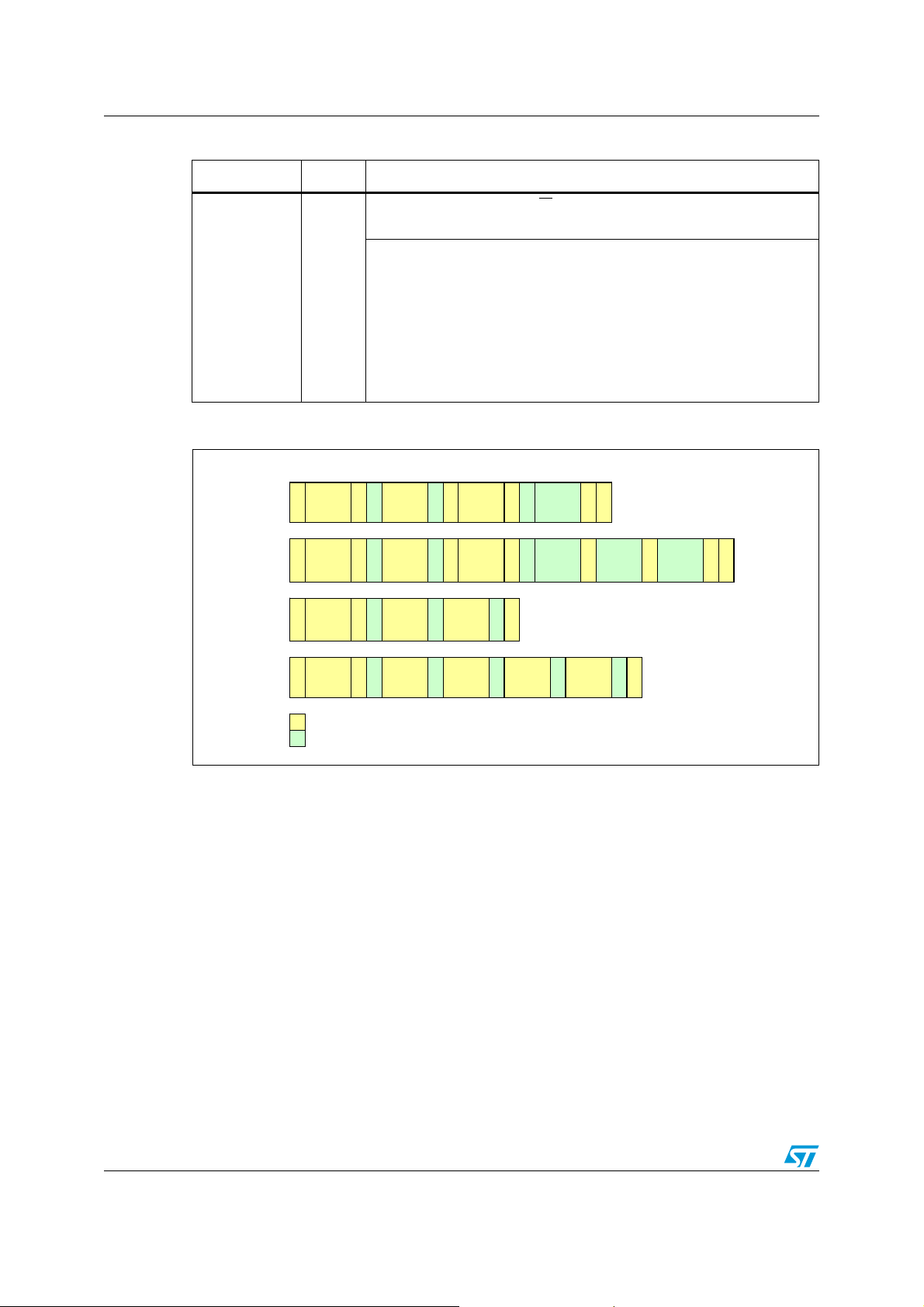
I2C specification STMPE1801
M
Table 9. Operating modes
Mode Byte Programming sequence
START, Device Address, R/W
=0, Register Address to be written, Data Write, STOP
If no STOP is issued, the Data Write can be continuously performed. If
the register address falls within the range that allows address autoincrement, then register address auto-increment internally after every
Write ≥1
byte of data being written. For those register addresses that fall within a
non-incremental address range, the address will be kept static
throughout the entire write operation. Refer to Table 8.: STMPE1801
register summary table for the address ranges that are auto-increment
and non-increment. An example of a non-increment address is Data
Port for initializing the PWM.
Figure 3. Operating modes
One B yte
Read
More than
One B yte
Read
One B yte
Write
ore than
One B yte
Write
Start
Start
Start
Start
Dev
Addr
Dev
Addr
Dev
Addr
Dev
Addr
Master
Slave
Reg
Addr
RnW=0
Ack
Reg
Addr
RnW=0
Ack
Reg
Addr
RnW=0
Ack
Reg
Addr
RnW=0
Ack
Ack
Ack
Ack
Ack
Dev
Addr
reStart
Dev
Addr
reStart
Data to
be
Written
Data to
Write
RnW=1
RnW=1
Ack
Stop
Data to
Write + 1
Ack
Dat a
Rea d
Ack
Ack
Dat a
Rea d
Data to
Write + 2
Ack
NoAck
Stop
Rea d + 1
Ack
Dat a
Ack
Stop
Rea d + 2
Ack
Dat a
NoAck
Stop
16/60 Doc ID 17884 Rev 3
Page 17
STMPE1801 I2C specification
6.9 General call address
A general call address is a transaction with the slave address of 0x00 and R/W =0. When a
general call address is asserted, the STMPE1801 responds to this transaction with an
acknowledgement and behaves as a slave-receiver mode. The meaning of a general call
address is defined in the second byte sent by the master-transmitter.
Table 10. General call address
R/W
Second byte
value
0 0x06
0 0x00 Not allowed as second byte.
A 2-byte transaction in which the second byte tells the slave device to reset
and write (or latch in) the 2-bit programmable part of the slave address.
Note: All other second byte values are ignored.
Definition
Doc ID 17884 Rev 3 17/60
Page 18
System controller STMPE1801
7 System controller
7.1 System level registers
The system controller is the heart of the STMPE1801. It contains the registers for power
control and chip identification.
The system registers are:
Address Register name
00 CHIP_ID
01 VERSION_ID
02 SYS_CTRL
CHIP_ID Chip identification register
76543 2 1 0
8-bit CHIP_ID
RRRRR R R R
11000 0 0 1
VERSION_ID Version identification register
76543 2 1 0
8-bit VERSION_ID
RRRRR R R R
00010 0 0 0
18/60 Doc ID 17884 Rev 3
Page 19

STMPE1801 System controller
SYS_CTRL System control register
76543 2 1 0
SF_RST RESERVED GPI_DB1 GPI_DB0 RSVD
WRRRR RW RW R
00000 1 1 0
Address: 02
Type: R/W
Reset: 0x06
Description: System control register.
[7] SF_RST: Soft Reset
Writing a ‘1’ to this bit will do a soft reset of the device. Once the reset is done, this bit is
cleared to ‘0’ by the HW.
[6:3] RESERVED
[2:1] GPI_DB [1:0]
GPI [17:0] operational mode de-bounce time
‘00’ = 30 µs
‘01’ = 90 µs
‘10’ = 150 µs
‘11’ = 210 µs (default)
[0] RESERVED
Doc ID 17884 Rev 3 19/60
Page 20

System controller STMPE1801
7.2 States of operation
Figure 4. States of operation
O perational
3 2 kHz: ON
No a ctivity
(~ 100 μs)
3 2 kHz: OFF
Hibernate
Keypad, interrupts
2
& I
C tran saction
(~ 48 μs)
Reset
AM04176V1
The device has two main modes of operation:
● Operational mode: This is the mode, whereby normal operation of the device takes
place. In this mode, the main finite state machine (FSM) unit routes 32 kHz clock to all
the device blocks.
● Hibernate mode: This mode is entered automatically in auto-hibernate mode. When the
device is in Hibernate mode, the 32 kHz clock is disabled. If there is a keypad activity,
interrupt event, hotkey activity or I
2
C transaction, the device switches to operational
mode. A reset event brings back the system to operational mode.
7.2.1 Auto-hibernate
The STMPE1801 is set to go into Hibernate mode automatically if there is a period of
inactivity (~ 100
STMPE1801 will continue counting down for hibernation mode activation even if there is an
2
I
C transaction sent by the host to other slave devices. Any I2C transaction from the host to
the STMPE1801 resets the hibernate counter.
Auto-hibernate mode occurs only when all the keys are released and FIFO is emptied
through reading. This is to prevent any loss of data.
The hibernate mode counter should start when any of the following conditions is detected:
– Once the I
– If the device ID in the I
When there is a keypad activity, the device should go into Hibernate mode ONLY when all
the previously pressed keys are released.
20/60 Doc ID 17884 Rev 3
µs) following the completion of I
2
C transaction is completed or a STOP condition is detected.
2
C transaction is invalid.
2
C transaction with the host. The
Page 21

STMPE1801 System controller
Any keypad activity, interrupt event, hotkey activity or VALID I2C transaction wakes up the
device from Hibernate mode and switches to operational mode automatically.
7.2.2 Keypress detect in the Hibernate mode
When in Hibernate mode, any keypress detected causes the system to go into operational
mode (~48
detected is valid, the system stays in operation mode. If the key detected is invalid, the
system goes back into Hibernate mode.
µs). The system will then de-bounce the key to detect a valid key. If the keypress
Doc ID 17884 Rev 3 21/60
Page 22

Clocking system STMPE1801
8 Clocking system
In order to reduce the power consumption, the STMPE1801 turns off the oscillator during
Hibernate mode.
Figure 5. Clocking system
K(Z
/3#
#LOCKCONTROL
3YSTEMCLOCK
8.0.1 Clock source
By default, when the STMPE1801 powers up, it derives a 32 kHz clock from the internal RC
oscillator for its operation.
There are 4 sources of reset:
● RSTB pin
● Low voltage detect (LVD) reset
● Soft reset bit of the SYS_CTRL register
2
● I
C reset from the I2C block.
3#,PIN
!-6
22/60 Doc ID 17884 Rev 3
Page 23

STMPE1801 Clocking system
8.0.2 Power mode programming sequence
The device enters auto Hibernate mode when there is inactivity for a fixed period of time.
To wake up the device, the host is required to:
– Send an I
To do a soft reset to the device, the host needs to do the following:
– Write a '1' to bit 7 of the SYS_CTRL register. This bit is automatically cleared upon
reset.
To come out of the Hibernate mode, the following needs to be done by the host:
– Assert a system reset
– Or put a wakeup on the I
– Interrupt activity
2
C transaction to the device.
2
C transaction
Doc ID 17884 Rev 3 23/60
Page 24

Interrupt system STMPE1801
9 Interrupt system
The STMPE1801 uses a highly flexible interrupt system. It allows the host system to
configure the type of system events that should result in an interrupt, and pinpoints the
source of interrupt by status registers. The INT pin can be configured as active high (a pulldown resistor is required), or active low (a pull-up resistor is required). If INT pin is not in
use, it is necessary to pull INT pin to V
Once asserted, the INT pin would de-assert when a read is done to the corresponding bit
either in the INT_STA register or INT_STA_GPIO register.
Figure 6. Interrupt system
CC
.
+EYPAD
CONTROLLER
'0)/
CONTROLLER
)NTERRUPT
ENABLE
'0)/
REGISTER
)NTERRUPTSTATUS
)NTERRUPTENABLE
REGISTER
REGISTER
)NTERRUPT
GENERATION
)NTERRUPTPOLARITYCONTROL
3YSTEMCONTROLREGISTER
!-6
24/60 Doc ID 17884 Rev 3
Page 25

STMPE1801 Interrupt system
9.1 Interrupt system register map
Table 11. Interrupt system register map
Address Register name Description
04 INT_CTRL_LOW
05 INT_CTRL_HIGH Yes
06 INT_EN_MASK_LOW
07 INT_EN_MASK_HIGH Yes
08 INT_STA_LOW
09 INT_STA_HIGH Yes
0A INT_EN_GPIO_MASK_LOW
0B INT_EN_GPIO_MASK_MID Yes
0C INT_EN_GPIO_MASK_HIGH Yes
0D INT_STA_GPIO_LOW
0E INT_STA_GPIO_MID Yes
0F INT_STA_GPIO_HIGH Yes
Interrupt control register
Interrupt enable mask register
Interrupt status register
Interrupt enable GPIO mask register
Interrupt status GPIO register
(during sequential R/W)
9.2 Interrupt latency for the GPIO hot keys
Auto-increment
Ye s
Ye s
Ye s
Ye s
Ye s
When the generation of interrupts by the GPIO as input is enabled for the hot keys, the
latency (time taken from actual transition at GPIO to time of INT pin assertion) is shown in
the following table:
Table 12. GPIO hot keys interrupt latency
State of operation Interrupt latency Comments
Hibernation >200 µs (default)
Active >200 µs (default)
Latency can be programmed by
the GPI_DB bits of SYS_CTRL
register
Doc ID 17884 Rev 3 25/60
Page 26

Interrupt system STMPE1801
INT_CTRL Interrupt control register
1514131211109876543 2 1 0
INT_CTRL_HIGH INT_CTRL_LOW
Reserved IC2 IC1 IC0
RRRRRRRRRRRRRRW RWRW
Address: 04, 05
Type: R, R/W
Reset: 0x00
Description: The interrupt control register is used to configure the interrupt controller. It has global
enable interrupt mask bit that controls the interruption to the host.
[15:3] RESERVED
[2] IC2: Output Interrupt polarity
‘0’ = Active low/falling edge
‘1’ = Active high/rising edge
[1] IC1: Output Interrupt type
‘0’ = Level interrupt
‘1’ = Edge interrupt (Pulse width of 200µs)
[0] IC0: Global interrupt mask bit
When this bit is written a ‘1’, it allows interruption to the host. If it is written with a ‘0’, then, it
disables all interruption to the host. Writing to this bit does not affect the INT_EN_MASK value.
26/60 Doc ID 17884 Rev 3
Page 27

STMPE1801 Interrupt system
INT_EN_MASK Interrupt enable mask register
1514131211109876543 2 1 0
INT_EN_MASK_HIGH INT_EN_MASK_LOW
RESERVED IE4 IE3 IE2 IE1 IE0
RRRRRRRRRRRRWRWRWRWRW
0000000000000 0 0 0
Address: 06, 07
Type: R, R/W
Reset: 0x00
Description: The interrupt enable mask register is used to enable the interruption from a particular
interrupt source to the host.
[15:4] RESERVED
[4:0] IE[x]:
Interrupt Enable Mask (where x = 3 to 0)
IE0: Default value is 0.
IE1: Keypad controller interrupt mask
IE2: Keypad controller FIFO overflow interrupt mask
IE3: GPIO controller interrupt mask
IE4: Combination key interrupt enable
Writing a ‘1’ to the IE[x] bit enables the interruption to the host.
Doc ID 17884 Rev 3 27/60
Page 28

Interrupt system STMPE1801
INT_STA Interrupt status register
1514131211109876543210
INT_STA_HIGH INT_STA _LOW
RESERVED IS4 IS3 IS2 IS1 IS0
RRRRRR RRRRRRRRRR
000000 0000000001
Address: 08, 09
Type: R
Reset: 0x00
Description: The interrupt status register monitors the status of the interruption from a particular
interrupt source to the host. The INT_STA bits are constantly updated regardless
whether the INT_EN bits are enabled or not.
[15:4] RESERVED
[4:0] IS[x]
Interrupt status (where x = 3 to 0)
Read:
IS0: Wake-up interrupt status
IS1: Keypad controller interrupt status
IS2: Keypad controller FIFO overflow interrupt status
IS3: GPIO controller interrupt status
IS4: Combination key interrupt status
Reading the INT_STA register clears all interrupt status bits to ‘0’ which had been set to ‘1’
prior to the read event.
28/60 Doc ID 17884 Rev 3
Page 29

STMPE1801 Interrupt system
INT_EN_GPIO_MASK Interrupt enabled GPIO mask register
76543 2 1 0
INT_EN_GPIO_MASK_LOW
IEG7 IEG6 IEG5 IEG4 IEG3 IEG2 IEG1 IEG0
RW RW RW RW RW RW RW RW
00000 0 0 0
15 14 13 12 11 10 9 8
INT_EN_GPIO_MASK_MID
IEG15 IEG14 IEG13 IEG12 IEG11 IEG10 IEG9 IEG8
RW RW RW RW RW RW RW RW
00000 0 0 0
23 22 21 20 19 18 17 16
INT_EN_GPIO_MASK_HIGH
Reserved IEG17 IEG16
R R R R R R RW RW
00000 0 0 0
Address: 0A, 0B, 0C
Type: R/W
Reset: 0x00
Description: The interrupt enable GPIO mask register is used to enable the interruption from a
particular GPIO interrupt source to the host. The IEG[17:0] bits are the interrupt
enable mask bits correspond to the GPIO[17:0] pins.
[17:0 IEG[x]: Interrupt enable GPIO mask (where x = 17 to 0)
Writing a ‘1’ to the IEG[x] bit enables the interruption to the host.
Doc ID 17884 Rev 3 29/60
Page 30

Interrupt system STMPE1801
NT_STA_GPIO Interrupt status GPIO register
76543 2 1 0
INT_STA_GPIO_LOW
ISG7 ISG6 ISG5 ISG4 ISG3 ISG2 ISG1 ISG0
RRRRR R R R
00000 0 0 0
15 14 13 12 11 10 9 8
INT_STA_GPIO_MID
ISG15 ISG14 ISG13 ISG12 ISG11 ISG10 ISG9 ISG8
RRRRR R R R
00000 0 0 0
23 22 21 20 19 18 17 16
INT_STA_GPIO_HIGH
Reserved ISG17 ISG16
RRRRR R R R
00000 0 0 0
Address: 0D, 0E, 0F
Type: R
Reset: 0x00
Description: The interrupt status GPIO register monitors the status of the interruption from a
particular GPIO pin interrupt source to the host. The INT_STA_GPIO bits are
constantly updated regardless whether the INT_EN_GPIO_MASK bits are enabled or
not. The ISG[17:0] bits are the interrupt status bits correspond to the GPIO[17:0] pins.
[17:0 ISG[x]
Interrupt status GPIO (where x = 17 to 0)
ISG[x] will be set to ‘1’ if an interrupt is detected on the corresponding GPIO pin.
Reading the INT_STA_GPIO register clears all interrupt status GPIO bits to ‘0’ which had been
set to ‘1’ prior to the read event.
30/60 Doc ID 17884 Rev 3
Page 31

STMPE1801 Interrupt system
9.3 Programming sequence
To configure and initialize the interrupt controller to allow interruption to host, observe the
following steps:
1. Set the INT_EN_MASK and INT_EN_GPIO_MASK registers to the desired values to
enable the interrupt sources that are to be expected to receive from.
2. Configure the output interrupt type and polarity and enable the global interrupt mask by
writing to the INT_CTRL.
3. Wait for interrupt.
4. Upon receiving an interrupt, the corresponding INT bit is asserted.
5. The host comes to read the INT_STA register through the I
INT_STA bits indicates that the corresponding interrupt source is triggered.
6. If the IS3 bit in INT_STA register is set, the interrupt is coming from the GPIO controller.
Then, a subsequent read is performed on the INT_STA_GPIO register to obtain the
interrupt status of all 18 GPIOs to locate the GPIO that triggers the interrupt. This is a
‘Hot Key’ feature.
7. After obtaining the interrupt source that triggers the interrupt, the host performs the
necessary processing and operations related to the interrupt source.
8. All IS[x] bits in INT_STA register and ISG[x] bits in INT_STA_GPIO register which are
set to ‘1’ prior to the read event are cleared to ‘0’ automatically once the reading of the
registers are completed.
9. Any interrupt inputs received between reading and auto clearing of the registers are
kept in a shadow register and updated into the INT_STA and INT_STA_GPIO registers
once the auto clearing is completed.
10. Once the interrupt is cleared, the INT pin is also de-asserted if the interrupt type is level
interrupt. An edge interrupt only asserts a pulse width of 200 µs.
11. When the interrupt function is no longer required, the IC0 bit in INT_CTRL may be set
to ‘0’ to disable the global interrupt mask bit.
2
C interface. A ‘1’ in the
Doc ID 17884 Rev 3 31/60
Page 32

GPIO controller STMPE1801
10 GPIO controller
A total of 18 GPIOs are available in the STMPE1801 port expander device. Most of the
GPIOs are sharing physical pins with alternate functions. The GPIO controller contains the
registers that allow the host system to configure each of the pins into either a GPIO, or one
of the alternate functions. Unused GPIOs should be configured as outputs to minimize the
power consumption.
Table 13. GPIO controller registers
Auto-increment
Address Register name Description
(during sequential
R/W)
10 GPIO_SET_LOW
11 GPIO_SET_MID Yes
12 GPIO_SET_HIGH Yes
13 GPIO_CLR_LOW
14 GPIO_CLR_MID Yes
15 GPIO_CLR_HIGH Yes
16 GPIO_MP_LOW
17 GPIO_MP_MID Yes
18 GPIO_MP_HIGH Yes
19 GPIO_SET_DIR_LOW
1A GPIO_SET_DIR_MID Yes
1B GPIO_SET_DIR_HIGH Yes
1C GPIO_RE_LOW
1D GPIO_RE_MID Yes
1E GPIO_RE_HIGH Yes
1F GPIO_FE_LOW
20 GPIO_FE_MID Yes
21 GPIO_FE_HIGH Yes
22 GPIO_PULL_UP_LOW
GPIO set pin state register
GPIO clear pin state register
GPIO monitor pin state register
GPIO set pin direction register
GPIO rising edge register
GPIO falling edge register
Ye s
Ye s
Ye s
Ye s
Ye s
Ye s
Ye s
23 GPIO_PULL_UP_MID Yes
24 GPIO_PULL_UP_HIGH Yes
32/60 Doc ID 17884 Rev 3
GPIO pull up register
Page 33
STMPE1801 GPIO controller
10.1 GPIO control registers
A group of registers is used to control the exact function of each of the 18 GPIOs.
All the GPIO registers are named as GPIO_xxx_yyy, where:
– xxx represents the functional group
– yyy represents the byte position of the GPIO (LOW/MID/HIGH)
– LOW registers control GPIO[7:0]
– MID registers control GPIO[8:15]
– HIGH registers control GPIO[17:16]
10.1.1 Bit description
76543 2 1 0
GPIO_xxx_HIGH RESERVED IO-16 IO-17
GPIO_xxx_MID IO-15 IO-14 IO-13 IO-12 IO-11 IO-10 IO-9 IO-8
GPIO_xxx_LOW IO-7 IO-6 IO-5 IO-4 IO-3 IO-2 IO-1 IO-0
The function of each bit is shown in the following table:
Register name Description Function
GPIO_MP_yyy GPIO monitor pin state
GPIO_SET_yyy GPIO set pin state
GPIO_CLR_yyy GPIO clear pin state
GPIO_SET_DIR_yyy GPIO set pin direction
GPIO_RE_yyy GPIO rising edge
GPIO_FE_yyy GPIO falling edge
GPIO_PULL_UP_yyy GPIO pull up Set to ‘1’ enable internal pull-up resistor.
Reading this bit yields the current state of the bit. Writing
has no effect.
Writing ‘1’ to this bit causes the corresponding GPIO to go
to ‘1’ state. Writing ‘0’ has no effect.
Writing ‘1’ to this bit causes the corresponding GPIO to go
to ‘0’ state. Writing ‘0’ has no effect.
‘0’ sets the corresponding GPIO to input state, and ‘1’ sets
it to output state.
Set to ‘1’ enable rising edge detection on the
corresponding GPIO.
Set to ‘1’ enable falling edge detection on the
corresponding GPIO.
Doc ID 17884 Rev 3 33/60
Page 34

GPIO controller STMPE1801
10.2 Hotkey feature
A GPIO is known as ‘Hotkey’ when it is configured to trigger an interruption to the host
whenever the GPIO input is being asserted. This feature is applicable in operational mode
as well as in Hibernate mode.
10.2.1 Programming sequence for Hotkey
1. Configure the GPIO pin into input direction by setting the corresponding bit in the GPIO
set pin direction registers [GPIO_SET_DIR_yyy].
2. Set the GPIO rising edge registers [GPIO_RE_yyy] and GPIO falling edge registers
[GPIO_FE_yyy] to the desired values to enable the rising edge or falling edge
detection.
3. Configure and enable the interrupt controller to allow the interruption to the host.
4. Now, the GPIO expander may enter Hibernate mode if there is no activity.
5. Upon any hot-key being asserted, the device will wake up and issue an interrupt to the
host.
Below are the conditions to be fulfilled in order to configure a Hot Key:
1. The pin is configured into GPIO mode and as input pin.
2. The global interrupt mask bit is enabled.
3. The corresponding GPIO interrupt mask bit is enabled.
10.2.2 Minimum pulse width
The minimum pulse width of the assertion of the Hotkey is dependent on the de-bounce
time configured. It must be greater than the de-bounce value configured. Any pulse width
less than the stated value may not be registered.
34/60 Doc ID 17884 Rev 3
Page 35

STMPE1801 Keypad controller
11 Keypad controller
The keypad controller consists of:
– 4 dedicated key controllers that support up to 4 simultaneous dedicated key
presses;
– a keyscan controller support a maximum of 10 x 8 key matrix with detection of
three simultaneous key presses;
– 8 special function key controllers that support up to 8 simultaneous “special
function” key presses.
The key detection priority is dedicated, special function and normal keys.
Four of the row inputs can be configured as dedicated keys through the setting of Dkey0~3
bits of the KPC_CTRL register. The normal key matrix size can be configured through the
setting of KPC_ROW and KPC_COL registers. The scanning of each individual row input
and column output can be enabled or masked to support a key matrix of variable size from 1
x 1 to 10 x 8. It is allowed to have other 8 special function keys incorporated in the key
matrix.
The operation of the keypad controller is enabled by the SCAN bit of KPC_CTRL register.
Every key activity detected is de-bounced for a period set by the DB_1~7 bits of KPC_CTRL
register before a key press or key release is confirmed and updated into the output FIFO.
The key data, indicating the key coordinates and its status (up or down), is loaded into the
FIFO at the end of a specified number of scanning cycles (set by SCAN_COUNT0~3 bits of
KPC_CTRL_MID register). An interrupt is generated when a new set of key data is loaded.
The FIFO has a capacity for ten sets of key data. Each set of key data consists of 5 bytes of
information when any of the four dedicated keys is enabled. It is reduced to 4 bytes when no
dedicated key is involved. When the FIFO is full before its content is read, an overflow signal
is generated while the FIFO will continue to hold its content but forbid loading of new key
data set.
Doc ID 17884 Rev 3 35/60
Page 36

Keypad controller STMPE1801
Figure 7. Keypad controller
/UTPUT
COLUMN
-ATRIXKEYPAD
)NPUTROW
!-6
The keypad rows enabled by the KPC_ROW register are normally 'high', with the
corresponding input pins pulled up by resistors internally. After reset, all the keypad columns
enabled by the KPC_COL register are driven 'low' via weak-pull down resistors. The pulldown resistors on the column are weaker than the pull-up resistors on the rows. If a key is
pressed, the stronger pull-up drive on the corresponding row overwrites the weaker pulldown drive on the selected column thus allowing the keyscan controller to sense a "high"
input on the selected column.
Once the keyscan controller senses a "high" on the selected column, the output buffer for
the selected column drives the line low overwriting the pull-up resistor on the corresponding
row. The row that senses the "low" signal enables the key scan controller to decode the key
coordinates (its corresponding row number and column number), save the key data into a
de-bounce buffer if available, confirm if it is a valid key press after de-bouncing, and update
the key data into output data FIFO if valid.
The key press/release detection mechanism is listed below:
1. When the GPIO is configured as keypad, the ROWS have internal "strong" pull-up and
COLUMNS have internal "weak" pull-down. The initial states of the ROWS are Logic
High and the COLUMNS are Logic Low.
2. When a keypad is pressed, the corresponding Row and Column form a Resistor
Voltage Divider Network. Since the pull-up resistance of the ROW is stronger than the
pull-down resistance of the COLUMN, the COLUMN is pulled to Logic High.
3. Once the COLUMN's state changes to Logic High, the state machine initiates a keyscan cycle and drives the selected COLUMN to Logic Low. A low is detected on the
36/60 Doc ID 17884 Rev 3
Page 37

STMPE1801 Keypad controller
key-press ROW. This is because the row and column node of key press are shorted
together.
4. The state machine continues to poll while the key is still pressed and is reinitialized
once all the keys are released.
The key detection sequence is described below:
1. The column outputs are initially not driven.
2. Then the row inputs are checked for any special function keys.
3. Next, the columns are checked for any normal key presses.
4. With the internal pull-down resistor on the columns, the column senses a logic low. But
when there is a normal key press, the pull up on the row and pull down on the column
forms a resistor voltage divider. Since the pull up resistor is sized much smaller than
the pull down resistor, the voltage on the column is pulled to logic high state.
5. Then only the configured columns that sensed a high are driven low in turn and check
for normal key presses.
This eliminates the need to drive columns that do not have any key press. This in turn
reduces the switching amount and hence the reduction in noise and EMI.
Also the 4 mA IO during GPIO mode is 1 mA in keypad mode.
Doc ID 17884 Rev 3 37/60
Page 38

Keypad controller STMPE1801
11.1 Keypad configurations
The keypad controller supports the following types of keys:
● Up to 10 columns * 8 rows matrix keys
● Up to 8 special function keys
● Up to 4 dedicated keys
Figure 8. Keypad configuration
Matrix keypad (10*8)
Input Row 0-7
10*8 (80) Matrix Keys
8 Special Function Keys
0 Dedicated Keys
STMPE1801
Output Column 0
-9
Special Function Keys
38/60 Doc ID 17884 Rev 3
!-6
Page 39

STMPE1801 Keypad controller
Figure 9. Keypad configurations
Matrix keypad (10*4)
STMPE1801
Output Column 0-9
Input Row 0-7
Dedicated Keys
Special Function Keys
10*4 (40) Matrix Keys
4 Special Function Keys
4 Dedicated Keys
!-6
Doc ID 17884 Rev 3 39/60
Page 40

Keypad controller STMPE1801
11.2 Keypad controller registers
The mapping between the keypad controller (rows and columns) and the GPIO is based on
Section 2.3.
Table 14. Keypad controller registers
Address Register name Description
30 KPC_ROW Keypad row register Yes
31 KPC_COL_LOW
32 KPC_COL_HIGH Yes
33 KPC_CTRL_LOW
34 KPC_CTRL_MID Yes
35 KPC_CTRL_HIGH Yes
36 KPC_CMD Key command register Yes
37 KPC_COMBI_KEY_0 Keypad combination key mask 0 Yes
38 KPC_COMBI_KEY_1 Keypad combination key mask 1 Yes
39 KPC_COMBI_KEY_2 Keypad combination key mask 2 Yes
3A KPC_DATA_BYTE0
3B KPC_DATA_BYTE1 Yes
3C KPC_DATA_BYTE2 Yes
3D KPC_DATA_BYTE3 Yes
3E KPC_DATA_BYTE4 Yes
Keypad column register
Keypad control register
Keypad data register
Auto-increment
(during sequential R/W)
Ye s
Ye s
Ye s
40/60 Doc ID 17884 Rev 3
Page 41

STMPE1801 Keypad controller
KPC_ROW Keypad controller row register
76543 2 1 0
Input Row 0 - 7
RW RW RW RW RW RW RW RW
00000 0 0 0
Address: 30
Type: R/W
Reset: 0x00
Description: Keypad row scanning
[7:0] Input row 0 – 7:
‘1’: Turn on scanning of the corresponding row
.‘0’: Turn off
KPC_COL_HIGH Keypad controller column (HIGH)
15 14 13 12 11 10 9 8
RESERVED Output Column 8 - 9
R R R R R R RW RW
00000 0 0 0
Address: 32
Type: R/W
Reset: 0x00
Description: Keypad column scanning register.
[15:10] RESERVED
[9:8] OUTPUT COLUMN 8-9:
‘1’: Turn on scanning of the corresponding column.
‘0’: Turn off
Doc ID 17884 Rev 3 41/60
Page 42
Keypad controller STMPE1801
KPC_COL_LOW Keypad controller column (LOW)
76543 2 1 0
Output Column 0 - 7
RW RW RW RW RW RW RW RW
00000 0 0 0
Address: 31
Type: R/W
Reset: 0x00
Description: Keypad column scanning register.
[7:0] OUTPUT COLUMN 0-7:
‘1’: Turn on scanning of the corresponding column.
‘0’: Turn off
KPC_CTRL_LOW Keypad controller control (Low)
76543 2 1 0
SCAN_COUNT 0 – 3 DKEY 0 – 3
RW RW RW RW RW RW RW RW
00000 0 0 0
Address: 33
Type: R/W
Reset: 0x00
Description: Keypad control register.
[7:4] SCAN_COUNT_0-3:
Number of key scanning cycles elapsed before a confirmed key data is updated into output
data FIFO (0-15 cycles)
[3] DKEY_3: Set ‘1’ to use input row 3 as dedicated key
[2] DKEY_2: Set ‘1’ to use input row 2 as dedicated key
[1] DKEY_1: Set ‘1’ to use input row 1 as dedicated key
[0] DKEY_0: Set ‘1’ to use input row 0 as dedicated key
42/60 Doc ID 17884 Rev 3
Page 43

STMPE1801 Keypad controller
KPC_CTRL_MID Keypad controller control (Mid)
76543 2 1 0
DB[7:2] DB0 RSVD
RW RW RW RW RW RW R RW
01100 0 1 0
Address: 34
Type: R/W
Reset: 0x31
Description: Keypad control register.
[7:1] DB[7:2] and DB0:
DB0 bit is fixed to ‘1’.
10-127ms of de-bounce time
De-bounce time range is from 10 ms to 127 ms with 50 ms as the default.
[0] RESERVED
Doc ID 17884 Rev 3 43/60
Page 44

Keypad controller STMPE1801
KPC_CTRL_HIGH Keypad controller control (High)
76543 2 1 0
RSVD CMB_KEY RESERVED SCAN_FREQ
RRWRRR R RW
01000 0 0 0
Address: 35
Type: R/W, R
Reset: 0x40
Description: Keypad data register.
[7:4] RESERVED
[6] CMB_KEY:
Combination key mode
1: AND function for combination-key interrupt (default).
0: OR function for combination-key interrupt.
[5:2] RESERVED
[1:0] SCAN_FREQ:
Scan frequency based on internal 32KHz clock
00: 60 Hz (default)
01: 30 Hz
10: 15 Hz
11: 275 Hz
KPC_CMD Keypad command register
76543 2 1 0
RSVD RSVD RSVD RSVD RSVD RSVD KPC_LOCK SCAN
R R R R R R RW RW
00000 0 0
Address: 36
Type: R/W, R
Reset: 0x00
Description: Keypad command register.
[7:2] RESERVED
[1] KPC_LOCK:
Keypad lock control bit
1: Writing 1 to enter key pad lock state when the key press stops.
44/60 Doc ID 17884 Rev 3
Page 45

STMPE1801 Keypad controller
The KPC_LOCK bit is only used when a combination key is configured in the device. If there
is no combination key programmed, then this bit is not used. This command is used in
conjunction with the combination keys. After the device has entered the keypad lock state,
all subsequent key presses are ignored until the combinational key(s) are detected.
Thereafter, the device exits the lock state, sets the combinational key wakeup status in the
interrupt status register bit IS[4] and sends out the interrupt if it was enabled.
0: Writing 0 aborts the key lock
Writing a 0 to this bit cancels any earlier key lock execution command. If the device has
already entered the lock state, writing 0 exits the lock state.
This bit is readable by the Host and the read status is described as follows:
Reading [1]: KPC lock execution is not completed. It is either waiting for the key press to
stop to enter the lock state or it is already in the lock state.
Reading [0]: KPC is already not in lock state, and not waiting to enter lock state.
[0]SCAN:
1: to start scanning
0: to stop
Note: All the key configurations and control must be completed before executing the scan
command. Any configuration and control change while scan is active is not supported.
Doc ID 17884 Rev 3 45/60
Page 46

Keypad controller STMPE1801
11.3 Data registers
The KPC_DATA register contains five bytes of information. The first three bytes store the key
coordinates and status of any three keys from the normal key matrix, while the fourth byte
stores the status of special function keys and the fifth byte consists of the status of
dedicated keys.
Note: When accessing the KPC DATA FIFO, it is mandatory to read all five bytes of KPC_Data
registers together consecutively.
46/60 Doc ID 17884 Rev 3
Page 47

STMPE1801 Keypad controller
KPC_DATA_BYTE0 Keypad data byte 0
76543 2 1 0
UP/DWN C3 C2 C1 C0 R2 R1 R0
RRRRR R R R
11111 0 0 0
Address: 3A
Type: R
Reset: 0xF8
Description: Keypad data register.
[7] UP/DWN:
0: key-down
1: key-up
[6:3] C[3:0]:
Column number of key 1 (valid range: 0000-1001)
0x1111: No key
[2:0] R[2:0]:
Row number of key 1 (valid range: 000-111)
KPC_DATA_BYTE1 Keypad data byte 1
76543 2 1 0
UP/DOWN C3 C2 C1 C0 R2 R1 R0
RRRRR R R R
11111 0 0 0
Address: 3B
Type: R
Reset: 0xF8
Description: Keypad data register.
[7] UP/DOWN:
0: key-down
1: key-up
[6:3] C[3:0]:
Column number of key 2 (valid range: 0000-1001)
0x1111: No key
[2:0] Row number of key 2 (valid range: 000-111)
Doc ID 17884 Rev 3 47/60
Page 48

Keypad controller STMPE1801
KPC_DATA_BYTE2 Keypad data byte 2
76543 2 1 0
UP/DOWN C3 C2 C1 C0 R2 R1 R0
RRRRR R R R
11111 0 0 0
Address: 3C
Type: R
Reset: 0xF8
Description: Keypad data register.
[7] UP/DOWN:
0: key-down
1: key-up
[6:3] C[3:0]: Column number of key 3 (valid range: 0000-1001)
0x1111: No key
[2:0] R[2:0]: Row number of key 3 (valid range: 000-111)
KPC_DATA_BYTE3 Keypad data byte 3
76543 2 1 0
SF7 SF6 SF5 SF4 SF3 SF2 SF1 SF0
RRRRR R R R
11111 1 1 1
Address: 3D
Type: R
Reset: 0xFF
Description: Keypad data register.
[7:0] SF[7:0]:
0: key-down
1: key-up
48/60 Doc ID 17884 Rev 3
Page 49

STMPE1801 Keypad controller
KPC_DATA_BYTE4 Keypad data byte 4
76543 2 1 0
RESERVED Dedicated Key 0 – 3
RRRRR R R R
00001 1 1 1
Address: 3E
Type: R
Reset: 0x0F
Description: Keypad data register.
[7:4] RESERVED
[3:0] Dedicated key [3:0]:
0: Key down
1: Key up
Doc ID 17884 Rev 3 49/60
Page 50

Keypad controller STMPE1801
11.4 Keypad combination key registers
The 3 keypad controller mask registers contains the key combination to be used to wake up
the KPC and send an interrupt to the host system.
KPC_COMB_KEY_n Keypad combination [n = 0-2]
76543 2 1 0
C4 C3 C2 C1 C0 R2 R1 R0
RW RW RW RW RW RW RW RW
11111 0 0 0
Address: 38, 39
Type: R/W
Reset: 0xF8
Description: Keypad combination key mask registers.
[7:3] C[4:0]: Column number of key n (valid range: 00000 – 01001)
[2:0] R[2:0]: Row number of key n (valid range: 000 – 111)
Valid key press value must be entered. The valid range for STMPE1801 is 00 to 4F. Any
other value outside this range is not accepted and a none value of F8 is returned.
50/60 Doc ID 17884 Rev 3
Page 51

STMPE1801 Keypad controller
11.5 Using the keypad controller
It is not necessary to explicitly enable the internal pull-up, pull-down and direction by
configuring the GPIO control registers. Once a GPIO is enabled for the keypad function, its
internal pull-up, pull-down and direction is controlled automatically.
The scanning of row inputs should then be enabled for those GPIO ports that are configured
as keypad inputs by writing '1's to the corresponding bits in the KPC_ROW register. If any of
the first four row inputs is to be used as dedicated key input, the corresponding bits in the
KPC_CTRL_MID register should be set to '1'. The bits in the KPC_COL_HIGH and
KPC_COL_LOW registers should also be set correctly to enable the column output
scanning for the corresponding GPIO ports programmed as keypad outputs.
The scan count and de-bounce count should also be programmed into the keypad control
registers before enabling the keypad controller operation. To enable the keypad controller
operation, the SCAN bit in the KPC_CTRL_LOW register must be set to '1'. The keypad
controller operation can be disabled by setting the SCAN bit back to '0'. The KPC interrupt
can be cleared upon status bit read, even if there is unread key-press in the KPC Data
register. It is the host responsibility to read the KPC Data register to access all key-press
data.
11.5.1 Ghost key handling
The ghost key is inherent in keypad matrix that is not equipped with a diode at each of the
keys. While it is not possible to avoid ghost key occurrence, the STMPE1801 allows the
detection of possible ghost keys by the capability of detecting 3 simultaneous key-presses in
the key matrix.
The ghost key is only possible if 3 keys are pressed and held down together in a keypad
matrix. If 3 keys are reported by the STMPE1801 keypad controller, it indicates a potential
ghost key situation. The system may check for the possibility of a ghost key by analyzing the
coordinates of the 3 keys. If the 3 keys form 3 corners of a rectangle, it could be a ghost key
situation.
A ghost key may also occur in the “special function keys”. The keypad controller does not
attempt to avoid the occurrence of ghost keys. However, the system should be aware that if
more than one special function key is reported, then there is a possibility of ghost keys.
11.5.2 Key detection priority
A dedicated key is always detected, if this is enabled. When a special function key is
detected, the matrix key scanning on the same input line is disabled.
Up to 3 matrix keys can be detected. Matrix keys that fall on activated special function keys
are not counted.
As a result of these priority rules, a matrix key is ignored by the keypad controller when the
special function key on the same input line is detected, even if the matrix key is being
pressed down before the special function key. Hence, when a matrix is reported "key-down"
and it is being held down while the corresponding special function is being pressed, a "no
key" status is reported for the matrix key when the special function key is reported "keydown". If the matrix key is released while the special function key is still being held down, no
"key-up" will be reported for the matrix key. On the other hand, if the matrix key is released
after the special function key is reported "key-up", then a new "key-down" is reported for the
matrix key, followed by "key-up".
Doc ID 17884 Rev 3 51/60
Page 52

Keypad controller STMPE1801
11.5.3 Keypad wakeup from Hibernate mode
The keypad controller is functional in Hibernate mode as long as it is enabled before
entering the Hibernate mode. It will then wake the system up into operational mode if a valid
key press is detected.
An asynchronous detection of the keypad column input activity is turned on during the
Hibernate mode. If any key activity is detected, the system wakes up into operational mode
for the de-bouncing of the key press to take place. If a valid key is detected, the system
stays in operational mode; otherwise, the device goes back into Hibernate mode.
11.5.4 Keypad controller combination key interrupt
The keypad controller (KPC) can be programmed to exit from Hibernate mode if a unique
combination keys is detected. These combination keys of up to 3 keys are specified in the
KPC combination set 0-2 registers.
There are 2 combination key operation modes. The modes can be set in the
COMB_KEY_MODE in the KPC_CTRL_HIGH register. In ‘OR’ mode, the device exits from
Hibernate mode on ANY of the 3 keys specified in the KPC combination set 0-2 registers. In
‘AND’ mode, the device exits from Hibernate mode ONLY if ALL of the 3 keys are pressed.
The sequence of the key pressed in not relevant as long as the 1-3 keys specified in the
KPC_COMB_KEY registers are detected, the KPC will exit from Hibernate mode and
interrupt the host. All the "active" keys must be pressed and held together, for the combi-key
interrupt to be generated.
If any other keys (beside those specified in the KPC_COMB_KEY_N registers) are pressed,
it would be considered an invalid combination and no interrupt will be generated.
52/60 Doc ID 17884 Rev 3
Page 53

STMPE1801 Miscellaneous features
12 Miscellaneous features
12.1 Reset
The STMPE1801 is equipped with an internal POR circuit that holds the device in reset
state, until the clock is steady and V
filter with minimum 180 ns at 1.8 V V
STMPE1801 by asserting the RSTB pin. The reset pin is also integrated with a filter of
minimum 200
µs duration and maximum 500 µs duration.
input is valid. The POR circuit is integrated with a
CC
. The host system may choose to reset the
CC
Doc ID 17884 Rev 3 53/60
Page 54

Package mechanical data STMPE1801
13 Package mechanical data
In order to meet environmental requirements, ST offers these devices in different grades of
ECOPACK
specifications, grade definitions and product status are available at: www.st.com.
ECOPACK
Figure 10. Package outline for Flip-chip CSP 25 (2.03 x 2.03 mm) - 0.4 mm pitch
®
packages, depending on their level of environmental compliance. ECOPACK®
®
is an ST trademark.
54/60 Doc ID 17884 Rev 3
Page 55

STMPE1801 Package mechanical data
Table 15. Package mechanical data for Flip-chip CSP 25 (2.03 x 2.03 mm)
0.4 mm pitch
Millimeters
Symbol
Min Typ Max
A 0.55 0.605 0.660
A1 0.17 0.205 0.24
A2 0.38 0.4 0.42
b 0.215 0.255 0.295
D1.9722.03
D1 - 1.6 -
E1.9722.03
E1 - 1.6 -
e 0.36 0.4 0.44
f 0.190 0.200 0.210
ccc - 0.05 0.05
Figure 11. Footprint recommendation
Doc ID 17884 Rev 3 55/60
Page 56

Package mechanical data STMPE1801
Figure 12. Device marking
)DENTIFICATIONFOR
DEVICEFRONTEND
ANDBACKENDPLANT
Figure 13. Carrier tape information
6,.
977
'
)DENTIFICATIONFOR
(ALOGENFREE
)DENTIFICATIONFOR
TRACEABLEDATECODE
!-6
1. Pin A1 is at top left corner based on above tape orientation.
56/60 Doc ID 17884 Rev 3
Page 57

STMPE1801 Package mechanical data
Table 16. Carrier tape specifications
Millimeters
Symbol
Min Typ Max
A0 2.06 2.11 2.16
B0 2.06 2.11 2.16
K0 0.64 0.69 0.74
F 3.45 3.50 3.55
W 7.90 8.00 8.30
P2 1.95 2.00 2.05
P0 3.90 4.00 4.10
10P0 39.80 40.00 40.20
D0 1.50 1.55 1.60
T 0.185 0.200 0.215
P 3.90 4.00 4.10
Table 17. Tape width (millimeters)
A N W1 W2 W3
Tape width
max min max max min max
8 180 60 8,4 14.4 7.9 10.9
Doc ID 17884 Rev 3 57/60
Page 58

Package mechanical data STMPE1801
Figure 14. Reel drawing (front)
Figure 15. Reel drawing (back)
58/60 Doc ID 17884 Rev 3
Page 59

STMPE1801 Revision history
14 Revision history
Table 18. Document revision history
Date Revision Changes
15-Nov-2010 1 Initial release.
13-Dec-2010 2 Updated: Figure 12 and added footnote related to Figure 13.
09-Mar-2011 3 Updated: Pin A1 function in Ta b le 2 and Section 12.1.
Doc ID 17884 Rev 3 59/60
Page 60

STMPE1801
Please Read Carefully:
Information in this document is provided solely in connection with ST products. STMicroelectronics NV and its subsidiaries (“ST”) reserve the
right to make changes, corrections, modifications or improvements, to this document, and the products and services described herein at any
time, without notice.
All ST products are sold pursuant to ST’s terms and conditions of sale.
Purchasers are solely responsible for the choice, selection and use of the ST products and services described herein, and ST assumes no
liability whatsoever relating to the choice, selection or use of the ST products and services described herein.
No license, express or implied, by estoppel or otherwise, to any intellectual property rights is granted under this document. If any part of this
document refers to any third party products or services it shall not be deemed a license grant by ST for the use of such third party products
or services, or any intellectual property contained therein or considered as a warranty covering the use in any manner whatsoever of such
third party products or services or any intellectual property contained therein.
UNLESS OTHERWISE SET FORTH IN ST’S TERMS AND CONDITIONS OF SALE ST DISCLAIMS ANY EXPRESS OR IMPLIED
WARRANTY WITH RESPECT TO THE USE AND/OR SALE OF ST PRODUCTS INCLUDING WITHOUT LIMITATION IMPLIED
WARRANTIES OF MERCHANTABILITY, FITNESS FOR A PARTICULAR PURPOSE (AND THEIR EQUIVALENTS UNDER THE LAWS
OF ANY JURISDICTION), OR INFRINGEMENT OF ANY PATENT, COPYRIGHT OR OTHER INTELLECTUAL PROPERTY RIGHT.
UNLESS EXPRESSLY APPROVED IN WRITING BY AN AUTHORIZED ST REPRESENTATIVE, ST PRODUCTS ARE NOT
RECOMMENDED, AUTHORIZED OR WARRANTED FOR USE IN MILITARY, AIR CRAFT, SPACE, LIFE SAVING, OR LIFE SUSTAINING
APPLICATIONS, NOR IN PRODUCTS OR SYSTEMS WHERE FAILURE OR MALFUNCTION MAY RESULT IN PERSONAL INJURY,
DEATH, OR SEVERE PROPERTY OR ENVIRONMENTAL DAMAGE. ST PRODUCTS WHICH ARE NOT SPECIFIED AS "AUTOMOTIVE
GRADE" MAY ONLY BE USED IN AUTOMOTIVE APPLICATIONS AT USER’S OWN RISK.
Resale of ST products with provisions different from the statements and/or technical features set forth in this document shall immediately void
any warranty granted by ST for the ST product or service described herein and shall not create or extend in any manner whatsoever, any
liability of ST.
ST and the ST logo are trademarks or registered trademarks of ST in various countries.
Information in this document supersedes and replaces all information previously supplied.
The ST logo is a registered trademark of STMicroelectronics. All other names are the property of their respective owners.
© 2011 STMicroelectronics - All rights reserved
STMicroelectronics group of companies
Australia - Belgium - Brazil - Canada - China - Czech Republic - Finland - France - Germany - Hong Kong - India - Israel - Italy - Japan -
Malaysia - Malta - Morocco - Philippines - Singapore - Spain - Sweden - Switzerland - United Kingdom - United States of America
www.st.com
60/60 Doc ID 17884 Rev 3
 Loading...