

STMAV335
Low ON Resistance Triple, SP3T, Wide-Bandwidth Video Switch
Features
■ Bi-directional operation
■ 3x3 input/3output channels analog video
switch
■ Wide bandwidth 300MHz
■ Low 4Ω swit ch resistance betw een two ports
■ Excellent R
■ Minimal propagation delay through the switch
■ Low quiescent current consumption
■ V
■ Zero bounce in flow-through mode
■ Control inputs compatible with TTL level
■ Data and control inputs provide the undershoot
Operating Range: 4.0V to 5.5V
CC
clamp diode
■ High ESD rating: > 2kV HBM
■ –40°C to 85°C operating temperature range
■ Suitable for both RGB and Component-Video
Switching
■ Available in a small TSSOP16 package
Applications
■ Advanced TVs
■ Front projectors
■ LCD Monitors
■ Notebook PCs
■ DVD Players
matching between channels
ON
TSSOP16
Description
The STMAV335 is a bi-directional triple (3
channel) Single Pole/Triple Throw (SP3T) highspeed, low-power CMOS TTL-compatible analog
video switch designed for advanced video
applications which demand superior image
quality. The low ON Resistance (R
switch allows inputs to be connected to outputs
without adding propagation delay or generating
additional ground bounce noise.
STMAV335 is designed for very low cross-talk,
low bit-to-bit skew, high channel-to-channel noise
isolation and low I/O capacitance. The switch
offers very little or practi cally no attenuation of the
high-speed signals at the outputs, thus preserving
the signal integrity to pass stringent requiremen ts.
Moreover the device reduces the overall BOM
costs by eliminating the need for more costly multi
input-output controllers.
) of the
ON
Order Codes
Part Number T em p erature Range Package Comments
STMAV335 –40°C to +85°C TSSOP16 STMAV335TTR
Rev . 1
January 2006 1/21
www.st.com
21

STMAV335
Contents
1 Summary Description . . . . . . . . . . . . . . . . . . . . . . . . . . . . . . . . . . . . . . . . . . 3
1.1 Functional Description . . . . . . . . . . . . . . . . . . . . . . . . . . . . . . . . . . . . . . . . . . 3
2 Pin Configuration . . . . . . . . . . . . . . . . . . . . . . . . . . . . . . . . . . . . . . . . . . . . . 4
3 Application Diagrams . . . . . . . . . . . . . . . . . . . . . . . . . . . . . . . . . . . . . . . . . . 5
3.1 Power Supply Sequencing . . . . . . . . . . . . . . . . . . . . . . . . . . . . . . . . . . . . . . . 5
4 Maximum Ratings . . . . . . . . . . . . . . . . . . . . . . . . . . . . . . . . . . . . . . . . . . . . . 6
5 Electrical Characteristics . . . . . . . . . . . . . . . . . . . . . . . . . . . . . . . . . . . . . . . 7
6 AC Loading and Diagrams . . . . . . . . . . . . . . . . . . . . . . . . . . . . . . . . . . . . . . 9
7 Test Circuits . . . . . . . . . . . . . . . . . . . . . . . . . . . . . . . . . . . . . . . . . . . . . . . . . 10
8 Package Mechanical D ata . . . . . . . . . . . . . . . . . . . . . . . . . . . . . . . . . . . . . . 17
9 Revision History . . . . . . . . . . . . . . . . . . . . . . . . . . . . . . . . . . . . . . . . . . . . . 20
2/21
STMAV335 1 Summary Description
1 Summary Description
1.1 Functional Description
The STMAV335 is a high bandwidth analog video switch. Its low ON-resistance and low I/O
capacitance result in a very small propagation delay.
The combination of SEL1 and SEL2 is used to either disable or enable the desired video
channel. Refer to the truth table for the selection of the appropriate channels.
Figure 1. Functional Diagr am
3/21
2 Pin Configuration STMAV335
2 Pin Configuration
Figure 2. Pin Config uration (Top View )
SEL1
SEL1
Y1
Y1
Y2
Y2
R
R
Pb1
Pb1
Pb2
Pb2
G
G
Pr/B
Pr/B
1
1
2
2
3
3
4
4
5
5
6
6
7
7
8
8
16
16
15
15
14
14
13
13
12
12
11
11
10
10
V
V
CC
CC
SEL2
SEL2
Y/R
Y/R
Pb/G
Pb/G
GND
GND
Pr1
Pr1
Pr2
Pr2
B
9
9
B
Table 1. Pin Description
Symbol Type Name and Functions
Bus Switch Enable. Tie to V
SEL1, SEL2 IN
Y/R, Pb/G, Pr/B IN/OUT Analog Video I/Os
Y1, Pb1, Pr1 IN/OUT Component 1; Anal og Video I/Os
Y2, Pb2, Pr2 IN/OUT Component 2; Anal og Video I/Os
R, G, B IN/OUT RGB or Component 3; Analog Video I/Os
V
CC
GND Ground
Table 2. Truth Table
SEL1 SEL2 Selection
0 0 Component = YPbPr1
0 1 Component = YPbPr2
1 0 Component = RGB
1 1 Switch disabled; external pull up resistor recommended
minimum value of t he res istor is det ermined by the cu rrent -sink ing
capability of t he driver.
Power supply
through a pull-up resis tor. The
CC
4/21
STMAV335 3 Application Diagrams
3 Application Diagrams
Figure 3. STMAV335 used in LCD TV as a 3-to-1 analog video switch
Figure 4. STMAV335 used in PC as a 1-to-3 analog video switch
3.1 Power Supply Sequencing
Proper power-supply sequencing is advised for all CMOS devices. It is recommended to
always apply V
before applying any signals to the input/output or control pins.
CC
5/21
4 Maximum Ratings STMAV335
4 Maximum Ratings
Stressing the device above the rating listed in the “A bsolu te Max imum Ratings” table may
cause permanent damage to the device. These are stress ratings only and operation of the
device at these or any other conditions above those indicated in the Operating sections of this
specification is not implied. Exposure to Absolute Maximum Rating conditions for extended
periods may affect device reliability. Refer also to the STMicroelectronics SURE Program and
other relevant quality documents.
Table 3. Absolute Maximum Ratings
T
= 25°C, VSS= 0V
A
Symbol Parameter Value Unit
V
I
ICC/I
T
CC
V
V
IN
I
IK
OUT
STG
S
GND
Supply Voltage -0.5 to + 7.0 V
DC Switch Vo lt age -0.5 to + 7.0 V
DC Input Voltage -0.5 to + 7.0 V
DC Input Diode Current -50 mA
DC Output Sink Current 128 mA
DC VCC/GND Current
St orage Temper ature Range -65 to 150 °C
±100 mA
Note: Absolute maximum ratings are those values above which damage to the device may occur.
Functional operation under these conditions is not implied. All voltages are referenced to GND.
6/21
STMAV335 5 Electrical Char acteristics
5 Electrical Characteristics
Table 4. Recommended Operating Conditions
= -20 to +70°C, V
T
A
SS
= 0V
Symbol Parameter (Note 1) T est Conditions M in. T yp. Max. Unit
V
V
V
V
OUT
t
T
Power Supply Vol tage 4.0 5.5 V
CC
Input Voltage 0 5.5 V
IN
Output Voltage 0 5.5 V
Input Rise and Fall Ti me
r, tf
Free Air Operating Temperature -40 +85 °C
A
ESD-Human Body Model (HBM) Note 2 -2 +2 kV
ESD
Switch Control Input 0 5 ns/V
Switch I/O 0 DC ns/V
Note: 1 Unused control inputs must be held HIGH or LOW. They should not float.
2 In accordance with IEC61000-4-2, level 4
Table 5. DC Electrical Characteristics
= -40°C to +85°C
T
A
V
Symbol Parameter Test Conditions
Analog Signal Range 5 0 2.0 V
I
V
V
V
Clamp Diode Voltage
IK
HIGH Level Input Voltage 4.0-5.5 2.0 V
IH
LOW Level Input Voltage 4.0-5.5 0.8 V
IL
I
Input Leakage Curr ent
I
= -18mA
IN
0 ≤ V
≤ 5.5V
IN
0 ≤ Y/R, Pb/G, Pr/B YX ≤ VCC,
I
R
∆I
OFF
ON
I
CC
OFF-STATE Leakage
Current
Switch ON resist ance (1)
Quiescent Supply Current
Increase in I
CC
per Input
CC
PbX ≤ V
, PrX ≤ V
CC
R ≤ VCC, G ≤ VCC , B ≤ V
VIN = 1.0V, ION = 13mA
= 2.0V, ION = 26mA
V
IN
V
IN = VCC
or GND, I
One input at 3.4V
Other inputs at V
CC
CC
OUT
or GN D
CC
= 0
(V)
CC
Min. Typ. Max. Unit
4.5 -1.2 V
5.5 ±10 µA
5.5 ±10 µA
4.5 3 7 Ω
4.5 7 10 Ω
5.5 3 µA
5.5 2.5 mA
Note: 1 Measured by the voltage drop between Y/R, Pb/G , Pr/B and YX/R, PbX/G, PrX/B pins at the
indicated current through the switch. ON Resistance is determined by the lower of the voltages
on the two.
7/21

5 Electrical Characteristi cs STMAV335
Table 6. AC Electrical Characteristics
= -40°C to +85°C, CL = 20pF, RU = RD = 75Ω
T
A
= 4.5 - 5.5V VCC = 4.0V
V
Symbol Parameter T est conditions
Output Enable Time Sel ect to Bus YX/
V
t
PZH
R, PbX/G, PrX/B
, t
PZL
Output Enable T ime Select to Bus Y/R,
= 7V for t
I
PZL
VI = OPEN for t
PHZ
Pb/G, Pr/B
Output Disable Time Select to Bus YX/
V
t
PHZ
R, PbX/G, PrX/B
, t
PLZ
Output Disable T ime, Output Enable
= 7V for t
I
PLZ
VI = OPEN for t
PHZ
time OE_N to Bus A, B/C
= 150Ω
R
L
= 25°C
T
A
= 10Ω
R
IN
= 150Ω, 10 MHz
R
L
= 150Ω
R
L
f = 3.58 MHz
= 150Ω
R
L
f = 3.58 MHz
= 150Ω
R
L
10 MHz
X
P
B
W
TALK
D
G
D
P
IRR
-3dB B andwidth
Crosstalk
Differenti al Gai n
Differenti al Phase
OFF Isolation
CC
Min. Typ. Max. Min. M ax.
5.2 5.7
5.1 5.6
5.2 5.5
5.5 5.5
300 MHz
-58 dB
0.64 %
0.1 Deg.
-60 dB
Unit
ns
ns
Table 7. Capacitance
= 25°C , f = 1MHz
T
A
Symbol Parameter Test Conditions Min. Typ. Max. Unit
V
C
Control Pin Input Cap acitance
IN
Input/Output Capacitance
C
Port: Y/R, Pb/G, Pr/B V
I/O
Input/Output Capacitance
Port: YX/R, PbX/G, PrX/B
C
Switch On Capacitance
ON
= 5.0V
CC
, SEL1,
CC
SEL2 = 5.0 V
V
= 5.0V,
CC
Except
SEL1,SEL2=5.0
3pF
7pF
5pF
12 pF
8/21
STMAV335 6 AC Loading and Diagrams
Ω
Ω
6 AC Loadin g and Diag ra m s
Figure 5. AC Test Circuit
V
V
I
I
RU
RU
FROM OUTPUT
FROM OUTPUT
UN DE R TEST
UN DE R TEST
20 pF
C
C
L
L
20 pF
RD 75
RD 75
Figure 6. AC Waveforms
tf= 2.5ns
tf= 2.5ns
90%
90%
ENABLE
ENABLE
INPU T
INPU T
t
t
PZL
PZL
t
t
PZH
PZH
1.5V
1.5V
OUTPUT
OUTPUT
10%
10%
OUTPUT
OUTPUT
1.5 V
1.5 V
1.5 V
1.5 V
10%
10%
90%
90%
1.5V
1.5V
t
t
= 2.5ns
= 2.5ns
r
r
GND
GND
t
t
PLZ
PLZ
t
t
PHZ
PHZ
3.0V
3.0V
VOL+ 0.3V
VOL+ 0.3V
V
V
OL
OL
V
V
OH
OH
VOH–0.3V
VOH–0.3V
9/21

7 Test Circuits STMAV335
7 Test Circuits
Figure 7. Test Circuit to measure the on-resistance of the switch
10/21

STMAV335 7 Test Circui ts
Figure 8. Enable/Disable Circuit and Timing Diagram
Table 8. Test Circuit
Test
Enable time
(tpZL, tpZH)
Disable Tim e
(tpLZ , tpHZ)
V
CC
4.75V ± 0.75V
4.75V ± 0.75V
4.75V ± 0.75V
4.75V ± 0.75V
4.75V ± 0.75V
4.75V ± 0.75V
R
75
75
75
75
75
75
L
C
L
20
20
20
20
20
20
V
Y1
GND
GND
V
CC
GND
GND
V
CC
Note: 1 CL includes probe and jig capacitance.
2 All input pulses are supplied by generators having the following characteristics: PRR
ZO = 50
Ω
, tr, tf = 2.5ns .
3 The outputs are measured one at a time, with one transition per measurement.
V
Pb1
GND
V
CC
GND
GND
V
CC
GND
V
Pr1
V
CC
GND
GND
V
CC
GND
GND
≤ 10MHz,
11/21

7 Test Circuits STMAV335
Differential gain and phase are measured at the output of the ON channel. For example, when
SEL1, SEL2 = 0 and Y is the input, the output is measured at Y1.
Figure 9. Differential Gain/Phase Measurement Test Circuit
12/21

STMAV335 7 Test Circui ts
Frequency response is measured at the output of the ON channel. For example, when
SEL1,SEL2 = 0, and Y is the input, the output is measured at Y1. All unused analog I/O ports
are left open.
Figure 10. Test Circuit for frequency response (BW)
13/21

7 Test Circuits STMAV335
Crosstalk is measured at the output of the non-adjacent ON channel. For example, when
SEL1,SEL2 = 0, and Y is the input, the output is measured at Pb1. All unused analog input
ports (Pb,Pr) and output ports (PbX,PrX) are connected to GND through 10Ω and 50Ω pulldown resistors respectively.
Figure 11. Crosstalk Test Circuit
Note: 50
14/21
Ω
termination resistor is needed for the network analyzer.

STMAV335 7 Test Circui ts
Off-Isolation is measured at the output of the OFF channel. For example, when SEL1=0,
SEL2=V
left open, and output ports are connected to GND through 50Ω pull-down resistors.
Figure 12. Off-Isolation Test Circuit
, and Y is the input, the output is measured at Y1. All unused analog input ports are
CC
Note: 50
Ω
termination resistor is needed for the network analyzer.
15/21
7 Test Circuits STMAV335
Figure 13. ESD protecti on c i rcuit for Input side of I/ O pi n
Figure 14. ESD protecti on ci rc u it fo r Ou tp ut s i de of I/O pi n
Figure 15. ESD protection circuit for SEL1, SEL2 inputs
16/21

STMAV335 8 Package Mechanical Data
8 Package M echanical Da ta
In order to meet environmental requirements, ST offers these devices in ECOPACK®
packages. These packages have a Lead-free second level interconnect . The category of
second Level Interconnect is marked on the package and on the inner box label, in compliance
with JEDEC Standard JESD97. The maximum ratings related to soldering conditions are also
marked on the inner box label. ECOPACK is an ST trademark. ECOPACK specifications are
available at: www.st.com.
17/21
8 Package Mechani cal Data STMAV335
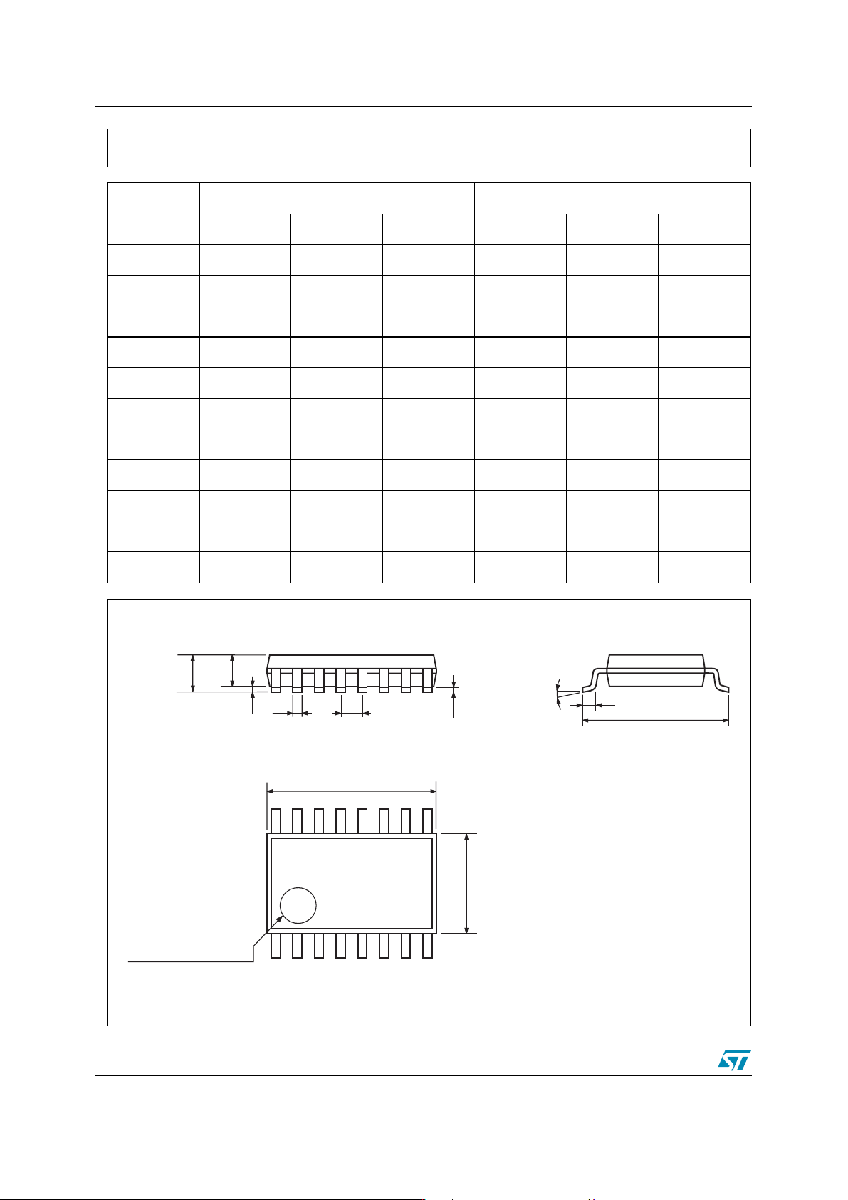
TSSOP16 MECHANICAL DATA
DIM.
mm inch
MIN. TYP. MAX. MIN. TYP. MAX.
A1.10.433
A1 0.05 0.10 0.15 0.002 0.004 0.006
A2 0.85 0.9 0.95 0.335 0.354 0.374
b 0.19 0.30 0.0075 0.0118
c 0.09 0.20 0.0035 0.0079
D 4.9 5 5.1 0.193 0.197 0.201
E 6.25 6.4 6.5 0.246 0.252 0.256
E1 4.3 4.4 4.48 0.169 0.173 0.176
e 0.65 BSC 0.0256 BSC
K0
o
o
4
o
8
o
0
o
4
o
8
L 0.50 0.60 0.70 0.020 0.024 0.028
A2
A
A1
b
e
D
PIN 1 IDENTIFICATION
1
18/21
K
c
L
E
E1
STMAV335 8 Package Mechanical Data
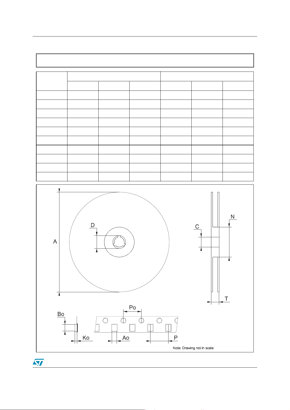
Tape & Reel TSSOP16 MECHANICAL DATA
DIM.
MIN. TYP MAX. MIN. TYP. MAX.
A 330 12.992
C 12.8 13.2 0.504 0.519
D 20.2 0.795
N 60 2.362
T 22.4 0.882
Ao 6.7 6.9 0.264 0.272
Bo 5.3 5.5 0.209 0.217
Ko 1.6 1.8 0.063 0.071
Po 3.9 4.1 0.153 0.161
P 7.9 8.1 0.311 0.319
mm. inch
19/21

9 Revision Hist ory STMAV335
9 Revision History
Date Revision Description of Chang e
23-Jan-2006 1 First Release
20/21

STMAV335 9 Revision History
I
s
o
d
b
ct
t
ot
a
nformation furnished is believed to be accurate and reliable. However, STMicroelectronics assumes no responsibility for the consequence
f use of such information nor for any infringement of patents or other rights of third parties which may result from its use. No license is grante
y implic ation or otherwise under any patent or patent ri ghts of STM i croelectr onics. Specifications menti oned in thi s publicati on are subje
o change without notice. This publication supersedes and replaces all information previously supplied. STMicroelectronics products are n
uthoriz ed for use as critical compo nents in life support devic es or systems without express writt en approval of STMicroel ectronics.
The ST logo is a registered t rademark of S TM i croelectr oni cs.
All other nam es are the pro perty of thei r respectiv e owners
© 2006 STMi croelectronics - All ri ght s reserved
Austra l i a - Be l gi um - Brazil - Canada - Chi na - Czech Rep ubl i c - Finland - F rance - Germ any - Hong Kon g - In di a - Israel - It aly - Japan -
Malaysi a - M al ta - Morocco - Singapore - Spain - Swe den - Switzerland - Un i te d Kingdom - United States of America
STMicroelectron ics group of com panies
www.st.com
21/21
 Loading...