How it Works
Log In / Sign Up
Buy Points
How it Works
FAQ
Contact Us
Questions and Suggestions
Users
ST
Loading...
S
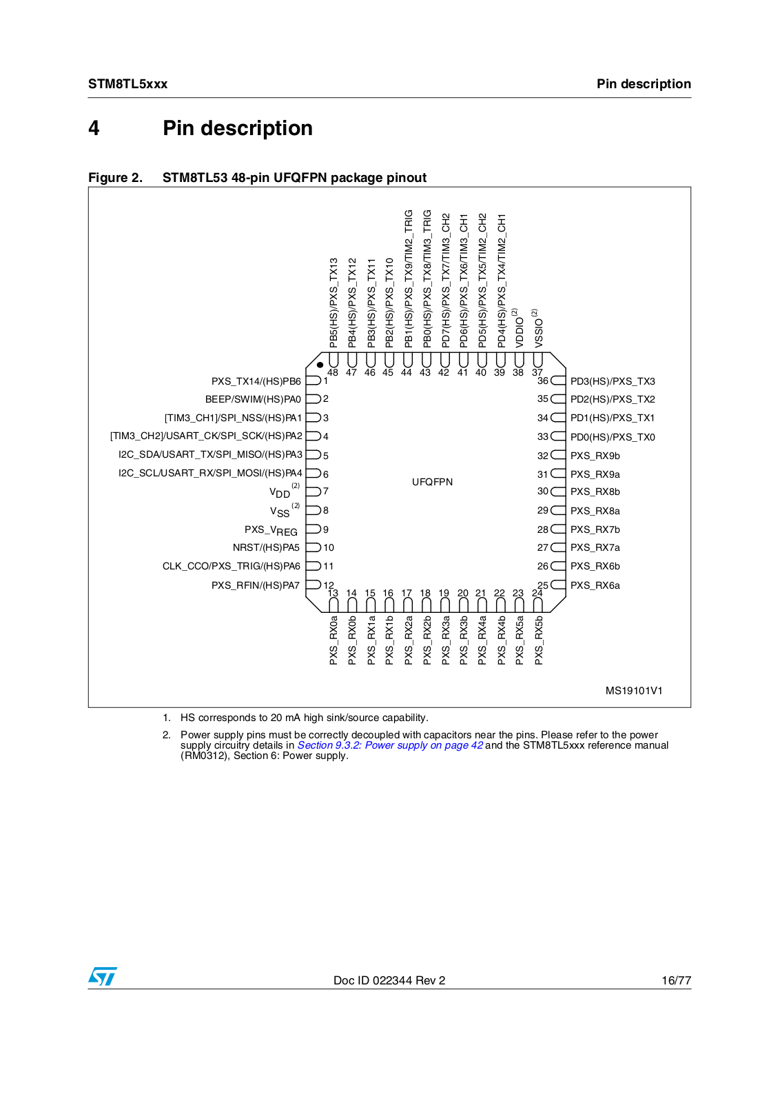
STM8L151C2
STM8L151C3
STM8L151F2
STM8L151F3
STM8L151G2
STM8L151G3
STM8L151K2
STM8L151K3
STM8L151R6
STM8L151x4
STM8L151x6
STM8L151x8
STM8L1526
STM8L1528
STM8L152R6
STM8L152x4
STM8L152x6
STM8L152x8
STM8L15LP
STM8L162M8
STM8L162R8
STM8S
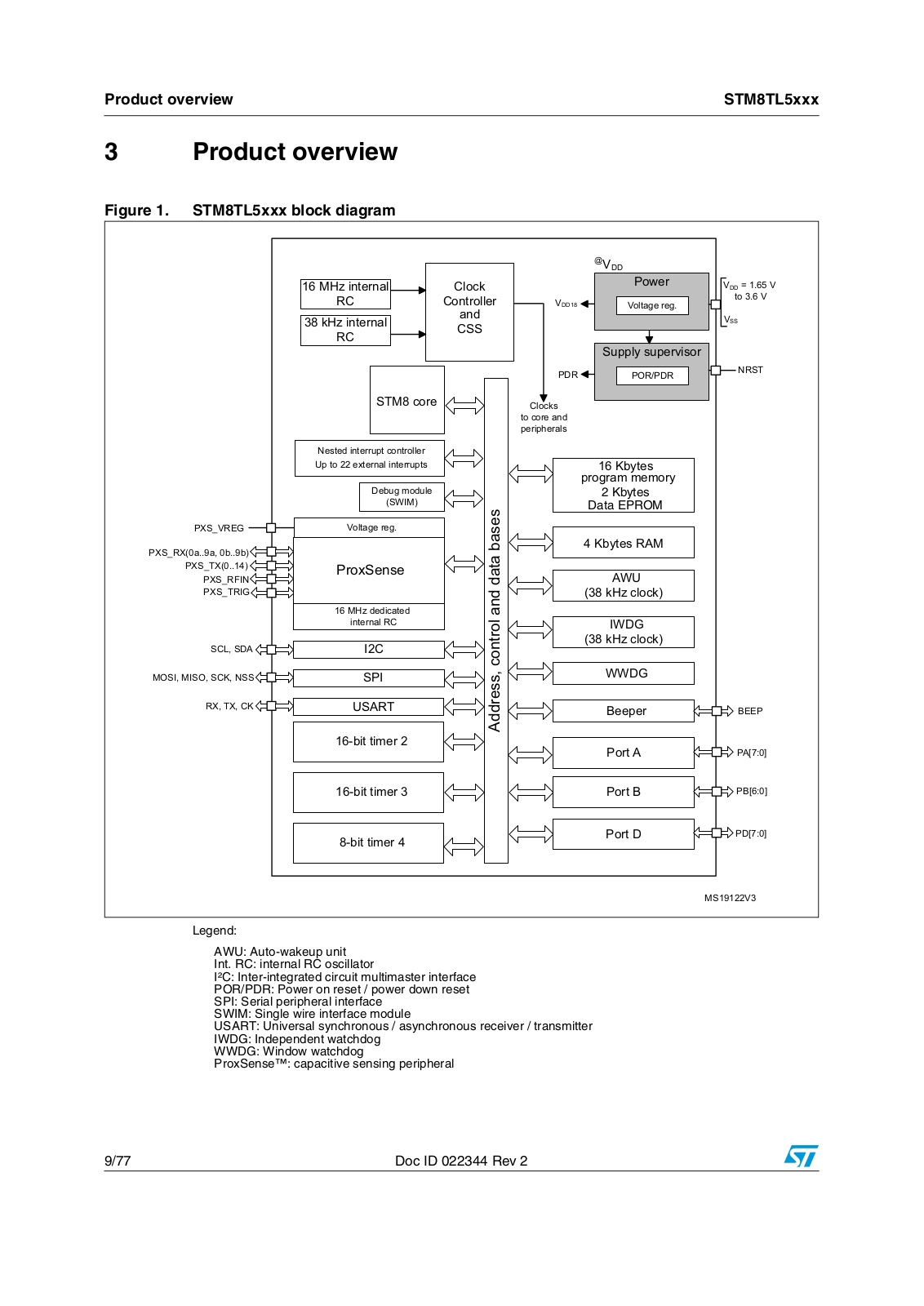
3
STM8S003F3
STM8S003K3
STM8S005C6
STM8S005K6
STM8S007C8
STM8S103F2
STM8S103F3
STM8S103K3
STM8S105C4
STM8S105C6
STM8S105K4
STM8S105K6
STM8S105S4
STM8S105S6
STM8S-32
STM8S-8
STM8S903F3
STM8S903K3
STM8SPLNB1
STM8SVL
STM8T141
2
STM8T143
2
STM8T14X-SB
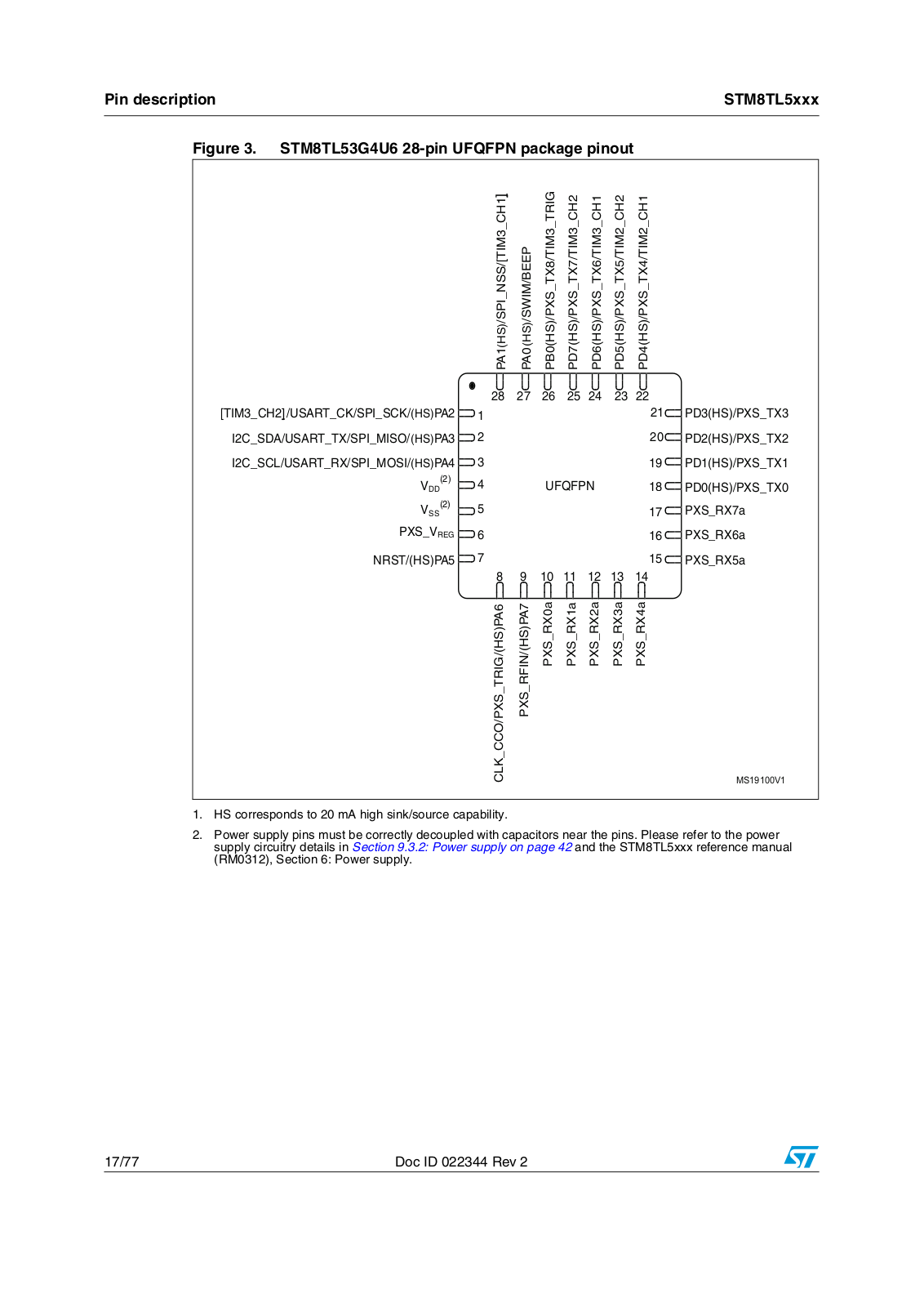
STM8TL52F4
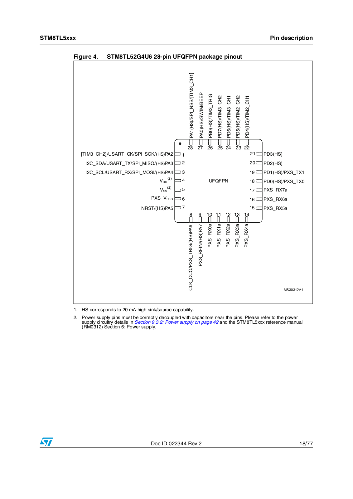
STM8TL52G4
STM8TL53C4
STM8TL53F4
STM8TL53G4
STM8T-MOD
STMAV335
STMAV340
STMPE1600
STMPE1601
STMPE1801
STMPE2403
STMPE610
STMPE801
STMPE811
STMPE812
STMPE812A
STMPRIMER
STMPS2141
STMPS2151
STMPS2161
STMPS2171
STMPS2242
STMPS2252
STMPS2262
STMPS2272
STMT05E
STMT07
STMUX1800E
STMUX1800L
STMUX3040
STMUX7000
STN715
STN724
STN817
STOD02
STOD03AS
STOD03B
STOD1317B
STOD13A
STOD13AS
STOD1812
STOD2540
STODD01
STODD03
STOTG04E
STOTG04ES
STP04CM05
STP04CM596
STP08C596
STP08CDC596
STP08CL596
STP08CP05
2
STP08DP05
STP100NF03L-03
Loading...
Loading...
Nothing found
STM8TL53G4
User Manual
77 pgs
1.04 Mb
0
Table of contents
Loading...
ST STM8TL52G4, STM8TL52F4, STM8TL53C4, STM8TL53G4, STM8TL53F4 User Manual
...
ST User Manual
Download
Specifications and Main Features
Frequently Asked Questions
User Manual
Download
Loading...
+
53
hidden pages
Unhide
You need points to download manuals.
1 point = 1 manual.
You can buy points or you can get point for every manual you upload.
Buy points
Upload your manuals
 Loading...