

Value line, 16 MHz STM8S 8-bit MCU, 32 Kbytes Flash, data
LQFP48 7x7
LQFP32 7x7
EEPROM,10-bit ADC, timers, UART, SPI, I²C
Features
Core
16 MHz advanced STM8 core with Harvard
•
architecture and 3-stage pipeline
Extended instruction set
•
Memories
Medium-density Flash/EEPROM:
•
Program memory: 32 Kbytes of Flash
-
memory; data retention 20 years at 55°C
after 100 cycles
Data memory: 128 bytes of true data
-
EEPROM; endurance up to 100 k write/erase
cycles
STM8S005K6 STM8S005C6
Permanently active, low consumption power-on
•
and power-down reset
Interrupt management
Nested interrupt controller with 32 interrupts
•
Up to 37 external interrupts on 6 vectors
•
Timers
2x 16-bit general purpose timers, with 2+3
•
CAPCOM channels (IC, OC or PWM)
Advanced control timer: 16-bit, 4 CAPCOM
•
channels, 3 complementary outputs, dead-time
insertion and flexible synchronization
8-bit basic timer with 8-bit prescaler
•
Auto wake-up timer
•
Window and independent watchdog timers
•
Communications interfaces
UART with clock output for synchronous
•
operation, Smartcard, IrDA, LIN
SPI interface up to 8 Mbit/s
•
I2C interface up to 400 Kbit/s
•
Analog-to-digital converter (ADC)
10-bit, ±1 LSB ADC with up to 10 multiplexed
•
channels, scan mode and analog watchdog
RAM: 2 Kbytes
•
Clock, reset and supply management
2.95 V to 5.5 V operating voltage
•
Flexible clock control, 4 master clock sources:
•
Low power crystal resonator oscillator
-
External clock input
-
Internal, user-trimmable 16 MHz RC
-
Internal low power 128 kHz RC
-
Clock security system with clock monitor
•
Power management:
•
Low power modes (wait, active-halt, halt)
-
Switch-off peripheral clocks individually
-
June 2012
I/Os
Up to 38 I/Os on a 48-pin package including 16
•
high sink outputs
Highly robust I/O design, immune against current
•
injection
Development support
Embedded single wire interface module (SWIM)
•
for fast on-chip programming and non intrusive
debugging
DocID022186 Rev 3
1/103
www.st.com

STM8S005K6 STM8S005C6Contents
Contents
1 Introduction ..............................................................................................................7
2 Description ...............................................................................................................8
3 Block diagram ..........................................................................................................9
4 Product overview ...................................................................................................10
4.1 Central processing unit STM8 .....................................................................................10
4.2 Single wire interface module (SWIM) and debug module (DM) ..................................10
4.3 Interrupt controller .......................................................................................................11
4.4 Flash program and data EEPROM memory ................................................................11
4.5 Clock controller ............................................................................................................12
4.6 Power management ....................................................................................................13
4.7 Watchdog timers ..........................................................................................................14
4.8 Auto wakeup counter ...................................................................................................14
4.9 Beeper ........................................................................................................................14
4.10 TIM1 - 16-bit advanced control timer .........................................................................15
4.11 TIM2, TIM3 - 16-bit general purpose timers ..............................................................15
4.12 TIM4 - 8-bit basic timer ..............................................................................................15
4.13 Analog-to-digital converter (ADC1) ............................................................................16
4.14 Communication interfaces .........................................................................................16
4.14.1 UART2 ...............................................................................................16
4.14.2 SPI .....................................................................................................17
4.14.3 I²C ......................................................................................................18
5 Pinout and pin description ...................................................................................19
5.1 STM8S005 pinouts and pin description .......................................................................20
5.1.1 Alternate function remapping ...............................................................24
6 Memory and register map .....................................................................................25
6.1 Memory map ................................................................................................................25
6.2 Register map ...............................................................................................................26
6.2.1 I/O port hardware register map ............................................................26
6.2.2 General hardware register map ...........................................................29
6.2.3 CPU/SWIM/debug module/interrupt controller registers ......................39
7 Interrupt vector mapping ......................................................................................42
8 Option bytes ...........................................................................................................44
9 Electrical characteristics ......................................................................................49
9.1 Parameter conditions ...................................................................................................49
9.1.1 Minimum and maximum values ...........................................................49
9.1.2 Typical values .......................................................................................49
9.1.3 Typical curves ......................................................................................49
DocID022186 Rev 32/103

ContentsSTM8S005K6 STM8S005C6
9.1.4 Typical current consumption ................................................................49
9.1.5 Loading capacitor .................................................................................50
9.1.6 Pin input voltage ...................................................................................50
9.2 Absolute maximum ratings ..........................................................................................50
9.3 Operating conditions ...................................................................................................52
9.3.1 VCAP external capacitor ......................................................................54
9.3.2 Supply current characteristics ..............................................................55
9.3.3 External clock sources and timing characteristics ...............................66
9.3.4 Internal clock sources and timing characteristics .................................68
9.3.5 Memory characteristics ........................................................................70
9.3.6 I/O port pin characteristics ...................................................................72
9.3.7 Typical output level curves ...................................................................75
9.3.8 Reset pin characteristics ......................................................................79
9.3.9 SPI serial peripheral interface ..............................................................81
9.3.10 I2C interface characteristics ...............................................................84
9.3.11 10-bit ADC characteristics ..................................................................86
9.3.12 EMC characteristics ...........................................................................89
10 Package information ...........................................................................................93
10.1 48-pin LQFP package mechanical data ....................................................................93
10.2 32-pin LQFP package mechanical data ....................................................................95
11 Thermal characteristics .......................................................................................97
11.1 Reference document .................................................................................................97
11.2 Selecting the product temperature range ..................................................................97
12 Ordering information ...........................................................................................99
13 STM8 development tools ..................................................................................100
13.1 Emulation and in-circuit debugging tools .................................................................100
13.2 Software tools ..........................................................................................................100
13.2.1 STM8 toolset ....................................................................................101
13.2.2 C and assembly toolchains ..............................................................101
13.3 Programming tools ..................................................................................................101
14 Revision history .................................................................................................102
3/103DocID022186 Rev 3

STM8S005K6 STM8S005C6List of tables
List of tables
Table 1. STM8S005xx value line features ................................................................................................8
Table 2. Peripheral clock gating bit assignments in CLK_PCKENR1/2 registers ..................................13
Table 3. TIM timer features ...................................................................................................................15
Table 4. Legend/abbreviations for pinout tables ...................................................................................19
Table 5. Pin description for STM8S005 microcontrollers .......................................................................21
Table 6. Flash, Data EEPROM and RAM boundary addresses ............................................................26
Table 7. I/O port hardware register map ................................................................................................26
Table 8. General hardware register map ................................................................................................29
Table 9. CPU/SWIM/debug module/interrupt controller registers ..........................................................39
Table 10. Interrupt mapping ...................................................................................................................42
Table 11. Option bytes ...........................................................................................................................44
Table 12. Option byte description ...........................................................................................................45
Table 13. Description of alternate function remapping bits [7:0] of OPT2 ..............................................47
Table 14. Voltage characteristics ...........................................................................................................50
Table 15. Current characteristics ...........................................................................................................51
Table 16. Thermal characteristics ..........................................................................................................52
Table 17. General operating conditions .................................................................................................53
Table 18. Operating conditions at power-up/power-down ......................................................................54
Table 19. Total current consumption with code execution in run mode at VDD= 5 V .............................55
Table 20. Total current consumption with code execution in run mode at VDD= 3.3 V ..........................66
Table 21. Total current consumption in wait mode at VDD= 5 V ............................................................58
Table 22. Total current consumption in wait mode at VDD= 3.3 V .........................................................58
Table 23. Total current consumption in active halt mode at VDD= 5 V ..................................................59
Table 24. Total current consumption in active halt mode at VDD= 3.3 V ...............................................60
Table 25. Total current consumption in halt mode at VDD= 5 V .............................................................61
Table 26. Total current consumption in halt mode at VDD= 3.3 V ..........................................................61
Table 27. Wakeup times .........................................................................................................................61
Table 28. Total current consumption and timing in forced reset state ....................................................92
Table 29. Peripheral current consumption .............................................................................................63
Table 30. HSE user external clock characteristics .................................................................................66
Table 31. HSE oscillator characteristics .................................................................................................67
Table 32. HSI oscillator characteristics ..................................................................................................68
Table 33. LSI oscillator characteristics ...................................................................................................70
Table 34. RAM and hardware registers ..................................................................................................70
Table 35. Flash program memory/data EEPROM memory ....................................................................71
Table 36. I/O static characteristics .........................................................................................................72
Table 37. Output driving current (standard ports) ..................................................................................74
Table 38. Output driving current (true open drain ports) ........................................................................74
Table 39. Output driving current (high sink ports) ..................................................................................74
Table 40. NRST pin characteristics ........................................................................................................79
Table 41. SPI characteristics ..................................................................................................................81
Table 42. I2C characteristics ..................................................................................................................84
Table 43. ADC characteristics ................................................................................................................86
Table 44. ADC accuracy with R
Table 45. ADC accuracy with R
Table 46. EMS data ................................................................................................................................90
Table 47. EMI data .................................................................................................................................91
< 10 kΩ , V
AIN
< 10 kΩ R
AIN
= 5 V .......................................................................87
DDA
AIN
, V
= 3.3 V ............................................................88
DDA
DocID022186 Rev 34/103

List of tablesSTM8S005K6 STM8S005C6
Table 48. ESD absolute maximum ratings .............................................................................................92
Table 49. Electrical sensitivities .............................................................................................................92
Table 50. 48-pin low profile quad flat package mechanical data ............................................................93
Table 51. 32-pin low profile quad flat package mechanical data .........................................................102
Table 52. Thermal characteristics
(1)
......................................................................................................97
Table 53. Document revision history ...................................................................................................102
5/103DocID022186 Rev 3

STM8S005K6 STM8S005C6List of figures
List of figures
Figure 1. STM8S005xx value line block diagram .....................................................................................9
Figure 2. Flash memory organization ....................................................................................................12
Figure 3. LQFP 48-pin pinout .................................................................................................................20
Figure 4. LQFP 32-pin pinout ................................................................................................................21
Figure 5. Memory map ...........................................................................................................................25
Figure 6. Supply current measurement conditions ................................................................................49
Figure 7. Pin loading conditions .............................................................................................................50
Figure 8. Pin input voltage .....................................................................................................................50
Figure 9. f
CPUmax
Figure 10. External capacitor C
Figure 11. Typ. I
Figure 12. Typ. I
Figure 13. Typ. I
Figure 14. Typ. I
Figure 15. Typ. I
Figure 16. Typ. I
Figure 17. HSE external clocksource .....................................................................................................67
Figure 18. HSE oscillator circuit diagram ...............................................................................................68
Figure 19. Typical HSI frequency variation vs VDD@ 3 temperatures ..................................................69
Figure 20. Typical LSI frequency variation vs VDD@ 3 temperatures ...................................................70
Figure 21. Typical VILand VIHvs VDD@ 3 temperatures ......................................................................73
Figure 22. Typical pull-up resistance vs VDD@ 3 temperatures ............................................................73
Figure 23. Typical pull-up current vs VDD@ 3 temperatures .................................................................73
Figure 24. Typ. VOL@ VDD= 5 V (standard ports) ................................................................................75
Figure 25. Typ. VOL@ VDD= 3.3 V (standard ports) .............................................................................76
Figure 26. Typ. VOL@ VDD= 5 V (true open drain ports) ......................................................................76
Figure 27. Typ. VOL@ VDD= 3.3 V (true open drain ports) ...................................................................76
Figure 28. Typ. VOL@ VDD= 5 V (high sink ports) ................................................................................77
Figure 29. Typ. VOL@ VDD= 3.3 V (high sink ports) .............................................................................77
Figure 30. Typ. VDD- VOH@ VDD= 5 V (standard ports) .......................................................................77
Figure 31. Typ. VDD- VOH@ VDD= 3.3 V (standard ports) ....................................................................78
Figure 32. Typ. VDD- VOH@ VDD= 5 V (high sink ports) ......................................................................78
Figure 33. Typ. VDD- VOH@ VDD= 3.3 V (high sink ports) ...................................................................78
Figure 34. Typical NRST VILand VIHvs VDD@ 3 temperatures ...........................................................80
Figure 35. Typical NRST pull-up resistance vs VDD@ 3 temperatures .................................................80
Figure 36. Typical NRST pull-up current vs VDD@ 3 temperatures ......................................................80
Figure 37. Recommended reset pin protection ......................................................................................81
Figure 38. SPI timing diagram - slave mode and CPHA = 0 ..................................................................83
Figure 39. SPI timing diagram - slave mode and CPHA = 1
Figure 40. SPI timing diagram - master mode
Figure 41. Typical application with I2C bus and timing diagram
Figure 42. ADC accuracy characteristics ...............................................................................................89
Figure 43. Typical application with ADC ................................................................................................89
Figure 44. 48-pin low profile quad flat package (7 x 7) ..........................................................................93
Figure 45. 32-pin low profile quad flat package (7 x 7) ..........................................................................95
Figure 46. STM8S005xx value line ordering information scheme .........................................................99
versus V
DD(RUN)
DD(RUN)
DD(RUN)
DD(WFI)
DD(WFI)
DD(WFI)
................................................................................................................54
DD
vs. V
vs. f
vs. V
vs. V
vs. f
DD ,
CPU ,
DD ,
DD ,
CPU
.......................................................................................................55
EXT
HSE user external clock, f
HSE user external clock, VDD= 5 V ..................................................64
HSI RC osc, f
HSE user external clock, f
, HSE user external clock VDD= 5 V ....................................................65
vs. VDD, HSI RC osc, f
= 16 MHz ...........................................64
CPU
= 16 MHz ..............................................................65
CPU
= 16 MHz ................................................................66
CPU
(1)
...................................................................................84
= 16 MHz ............................................65
CPU
(1)
.............................................................83
(1)
.......................................................85
DocID022186 Rev 36/103

IntroductionSTM8S005K6 STM8S005C6
Introduction1
This datasheet contains the description of the device features, pinout, electrical characteristics,
mechanical data and ordering information.
For complete information on the STM8S microcontroller memory, registers and peripherals,
•
please refer to the STM8S microcontroller family reference manual (RM0016).
For information on programming, erasing and protection of the internal Flash memory
•
please refer to the STM8S Flash programming manual (PM0051).
For information on the debug and SWIM (single wire interface module) refer to the STM8
•
SWIM communication protocol and debug module user manual (UM0470).
For information on the STM8 core, please refer to the STM8 CPU programming manual
•
(PM0044).
7/103DocID022186 Rev 3
STM8S005K6 STM8S005C6Description
Description2
The STM8S005xx value line 8-bit microcontrollers offer 32 Kbytes of Flash program memory,
plus 128 bytes of data EEPROM. They are referred to as medium-density devices in the
STM8S microcontroller family reference manual (RM0016). All devices of the STM8S005xx
value line provide the following benefits: performance, robustness, reduced system cost, and
short develoment cycles.
Device performance and robustness are ensured by true data EEPROM supporting up to 100
000 write/erase cycles, advanced core and peripherals made in a state-of-the art technology,
a 16 MHz clock frequency, robust I/Os, independent watchdogs with separate clock source,
and a clock security system.
The system cost is reduced thanks to high system integration level with internal clock
oscillators, watchdog and brown-out reset.
Common family product architecture with compatible pinout, memory map and modular
peripherals allow application scalability and reduced development cycles.
All products operate from a 2.95 to 5.5 V supply voltage.
Full documentation is offered as well as a wide choice of development tools.
Table 1: STM8S005xx value line features
STM8S005K6STM8S005C6Device
3248Pin count
(bytes)
Peripheral set
2538Maximum number of GPIOs
2335Ext. Interrupt pins
89Timer CAPCOM channels
33Timer complementary outputs
710A/D Converter channels
1216High sink I/Os
32K32KMedium density Flash Program memory
128128Data EEPROM (bytes)
2K2KRAM (bytes)
Advanced control timer (TIM1), General-purpose timers (TIM2 and TIM3), Basic
timer (TIM4) SPI, I2C, UART, Window WDG, Independent WDG, ADC
DocID022186 Rev 38/103
XTAL 1-16 MHz
RC int. 16 MHz
RC int. 128 kHz
STM8 core
Debug/SWIM
I2C
SPI
UART2
16-bit general purpose
AWU timer
Reset block
Reset
POR/
PDR
BOR
Clock controller
Detector
Clock to peripherals and core
8 Mbit/s
Address and data bus
Window WDG
Independent WDG
32 Kbytes
128 bytes
2 Kbytes
Boot ROM
ADC1
Reset
400 Kbit/s
Single wire
debug interf.
program Flash
16-bit advanced control
timer (TIM1)
timers (TIM2, TIM3)
8-bit basic timer
(TIM4)
data EEPROM
RAM
Master/slave
autosynchro
LIN master
SPI emul.
Beeper
1/2/4 kHz
beep
5 CAPCOM
channels
Up to
4 CAPCOM
channels +3
Up to
complementary
outputs
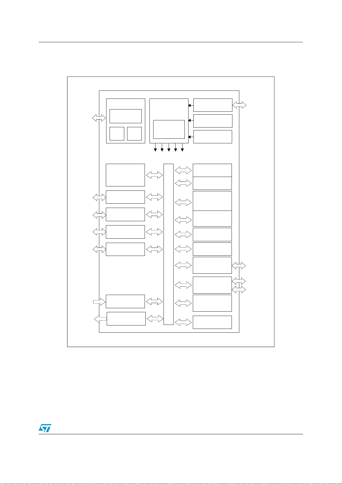
Block diagramSTM8S005K6 STM8S005C6
Block diagram3
Figure 1: STM8S005xx value line block diagram
9/103DocID022186 Rev 3

STM8S005K6 STM8S005C6Product overview
Product overview4
The following section intends to give an overview of the basic features of the device functional
modules and peripherals.
For more detailed information please refer to the corresponding family reference manual
(RM0016).
Central processing unit STM84.1
The 8-bit STM8 core is designed for code efficiency and performance.
It contains 6 internal registers which are directly addressable in each execution context, 20
addressing modes including indexed indirect and relative addressing and 80 instructions.
Architecture and registers
Harvard architecture
•
3-stage pipeline
•
32-bit wide program memory bus - single cycle fetching for most instructions
•
X and Y 16-bit index registers - enabling indexed addressing modes with or without offset
•
and read-modify-write type data manipulations
8-bit accumulator
•
24-bit program counter - 16-Mbyte linear memory space
•
16-bit stack pointer - access to a 64 K-level stack
•
8-bit condition code register - 7 condition flags for the result of the last instruction
•
Addressing
20 addressing modes
•
Indexed indirect addressing mode for look-up tables located anywhere in the address
•
space
Stack pointer relative addressing mode for local variables and parameter passing
•
Instruction set
80 instructions with 2-byte average instruction size
•
Standard data movement and logic/arithmetic functions
•
8-bit by 8-bit multiplication
•
16-bit by 8-bit and 16-bit by 16-bit division
•
Bit manipulation
•
Data transfer between stack and accumulator (push/pop) with direct stack access
•
Data transfer using the X and Y registers or direct memory-to-memory transfers
•
Single wire interface module (SWIM) and debug module (DM)4.2
The single wire interface module and debug module permits non-intrusive, real-time in-circuit
debugging and fast memory programming.
DocID022186 Rev 310/103

Product overviewSTM8S005K6 STM8S005C6
SWIM
Single wire interface module for direct access to the debug module and memory programming.
The interface can be activated in all device operation modes. The maximum data transmission
speed is 145 bytes/ms.
Debug module
The non-intrusive debugging module features a performance close to a full-featured emulator.
Beside memory and peripherals, also CPU operation can be monitored in real-time by means
of shadow registers.
R/W to RAM and peripheral registers in real-time
•
R/W access to all resources by stalling the CPU
•
Breakpoints on all program-memory instructions (software breakpoints)
•
Two advanced breakpoints, 23 predefined configurations
•
Interrupt controller4.3
Nested interrupts with three software priority levels
•
32 interrupt vectors with hardware priority
•
Up to 37 external interrupts on 6 vectors including TLI
•
Trap and reset interrupts
•
Flash program and data EEPROM memory4.4
32 Kbytes of Flash program single voltage Flash memory
•
128 bytes true data EEPROM
•
Read while write: Writing in data memory possible while executing code in program memory
•
User option byte area
•
Write protection (WP)
Write protection of Flash program memory and data EEPROM is provided to avoid unintentional
overwriting of memory that could result from a user software malfunction.
There are two levels of write protection. The first level is known as MASS (memory access
security system). MASS is always enabled and protects the main Flash program memory,
data EEPROM and option bytes.
To perform in-application programming (IAP), this write protection can be removed by writing
a MASS key sequence in a control register. This allows the application to write to data
EEPROM, modify the contents of main program memory or the device option bytes.
A second level of write protection, can be enabled to further protect a specific area of memory
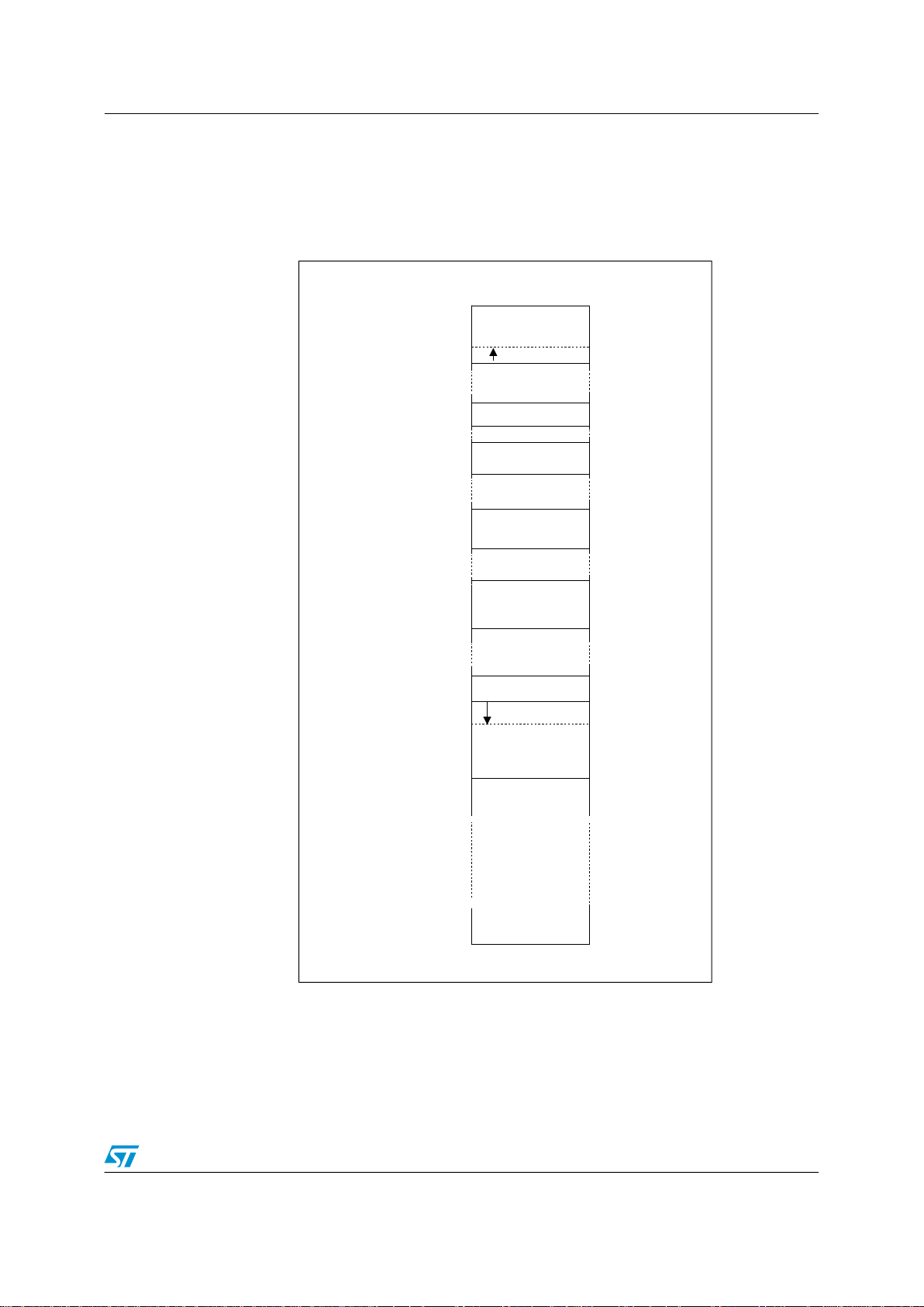
known as UBC (user boot code). Refer to the figure below.
The size of the UBC is programmable through the UBC option byte, in increments of 1 page
(512 bytes) by programming the UBC option byte in ICP mode.
This divides the program memory into two areas:
Main program memory: 32 Kbytes minus UBC
•
User-specific boot code (UBC): Configurable up to 32 Kbytes
•
11/103DocID022186 Rev 3
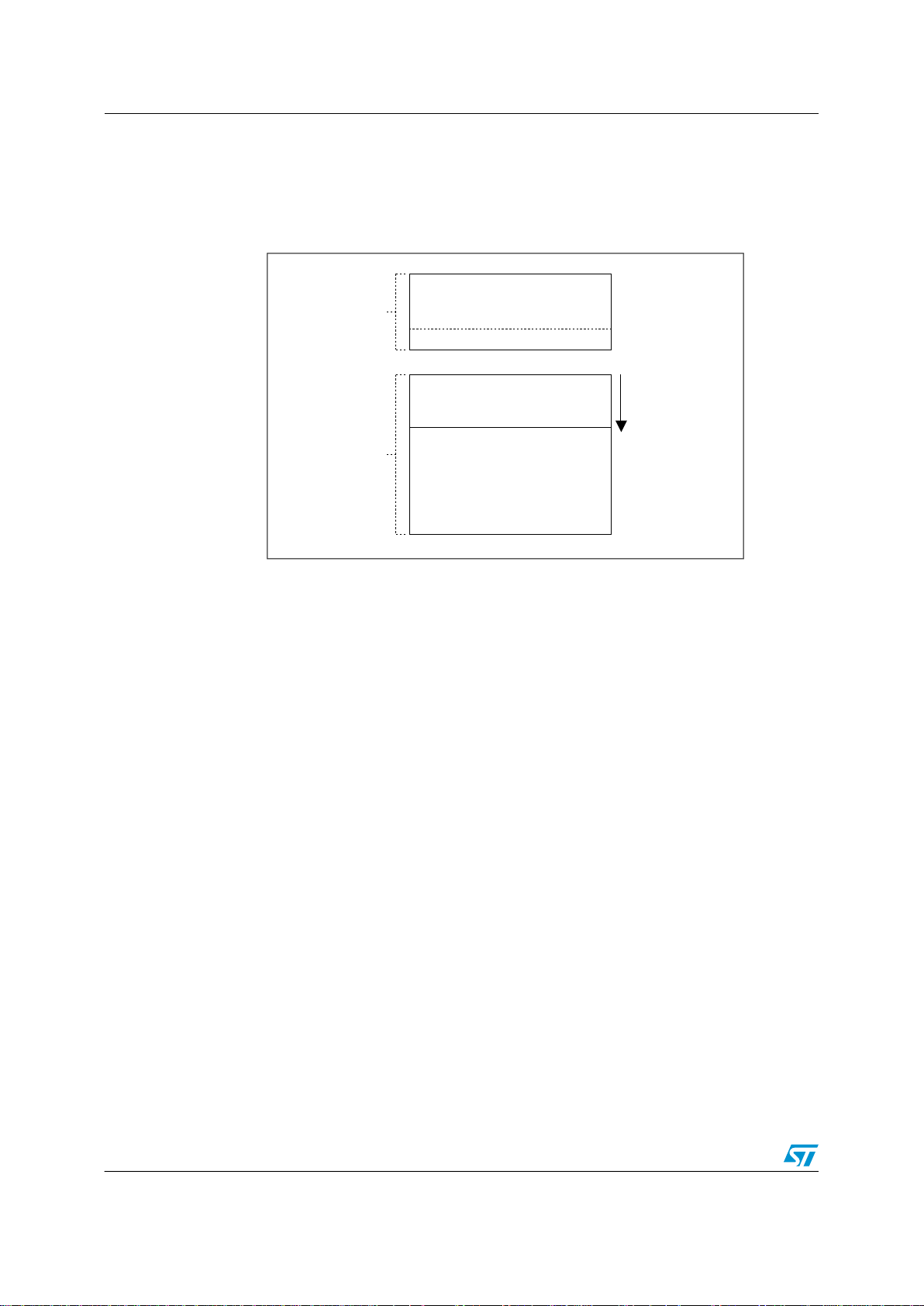
Programmable area
Data
Program memory area
Data memory area ( 128 bytes)
EEPROM
UBC area
Remains write protected during IAP
memory
Write access possible for IAP
(1 page steps)
Option bytes
(2 first pages) up to
Medium density
Flash program memory
(32 Kbytes)
from 1 Kbyte
32 Kbytes
STM8S005K6 STM8S005C6Product overview
The UBC area remains write-protected during in-application programming. This means that
the MASS keys do not unlock the UBC area. It protects the memory used to store the boot
program, specific code libraries, reset and interrupt vectors, the reset routine and usually the
IAP and communication routines.
Figure 2: Flash memory organization
Read-out protection (ROP)
The read-out protection blocks reading and writing the Flash program memory and data
EEPROM memory in ICP mode (and debug mode). Once the read-out protection is activated,
any attempt to toggle its status triggers a global erase of the program and data memory. Even
if no protection can be considered as totally unbreakable, the feature provides a very high
level of protection for a general purpose microcontroller.
Clock controller4.5
The clock controller distributes the system clock (f
to the core and the peripherals. It also manages clock gating for low power modes and ensures
clock robustness.
Features
Clock prescaler: To get the best compromise between speed and current consumption
•
the clock frequency to the CPU and peripherals can be adjusted by a programmable
prescaler.
Safe clock switching: Clock sources can be changed safely on the fly in run mode
•
through a configuration register. The clock signal is not switched until the new clock source
is ready. The design guarantees glitch-free switching.
Clock management: To reduce power consumption, the clock controller can stop the
•
clock to the core, individual peripherals or memory.
Master clock sources: Four different clock sources can be used to drive the master
•
clock:
1-16 MHz high-speed external crystal (HSE)
-
Up to 16 MHz high-speed user-external clock (HSE user-ext)
-
MASTER
) coming from different oscillators
DocID022186 Rev 312/103
Product overviewSTM8S005K6 STM8S005C6
16 MHz high-speed internal RC oscillator (HSI)
-
128 kHz low-speed internal RC (LSI)
-
Startup clock: After reset, the microcontroller restarts by default with an internal 2 MHz
•
clock (HSI/8). The prescaler ratio and clock source can be changed by the application
program as soon as the code execution starts.
Clock security system (CSS): This feature can be enabled by software. If an HSE clock
•
failure occurs, the internal RC (16 MHz/8) is automatically selected by the CSS and an
interrupt can optionally be generated.
Configurable main clock output (CCO): This outputs an external clock for use by the
•
application.
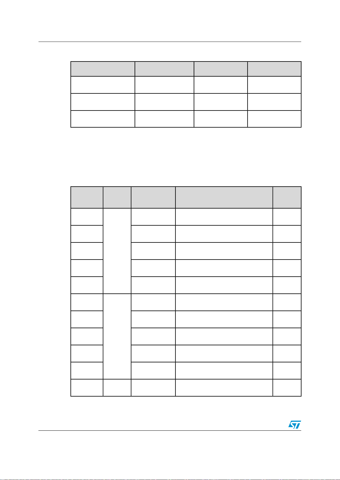
Table 2: Peripheral clock gating bit assignments in CLK_PCKENR1/2 registers
Bit
Peripheral
clock
ADCPCKEN2 3ReservedPCKEN2 7UART2PCKEN1 3TIM1PCKEN1 7
AWUPCKEN2 2ReservedPCKEN2 6ReservedPCKEN1 2TIM3PCKEN1 6
ReservedPCKEN2 1ReservedPCKEN2 5SPIPCKEN1 1TIM2PCKEN1 5
ReservedPCKEN2 0ReservedPCKEN2 4I2CPCKEN1 0TIM4PCKEN1 4
clock
BitPeripheral
clock
BitPeripheral
clock
BitPeripheral
Power management4.6
For efficent power management, the application can be put in one of four different low-power
modes. You can configure each mode to obtain the best compromise between lowest power
consumption, fastest start-up time and available wakeup sources.
Wait mode: In this mode, the CPU is stopped, but peripherals are kept running. The
•
wakeup is performed by an internal or external interrupt or reset.
Active halt mode with regulator on: In this mode, the CPU and peripheral clocks are
•
stopped. An internal wakeup is generated at programmable intervals by the auto wake up
unit (AWU). The main voltage regulator is kept powered on, so current consumption is
higher than in active halt mode with regulator off, but the wakeup time is faster. Wakeup
is triggered by the internal AWU interrupt, external interrupt or reset.
Active halt mode with regulator off: This mode is the same as active halt with regulator
•
on, except that the main voltage regulator is powered off, so the wake up time is slower.
Halt mode: In this mode the microcontroller uses the least power. The CPU and peripheral
•
clocks are stopped, the main voltage regulator is powered off. Wakeup is triggered by
external event or reset.
13/103DocID022186 Rev 3

STM8S005K6 STM8S005C6Product overview
Watchdog timers4.7
The watchdog system is based on two independent timers providing maximum security to
the applications.
Activation of the watchdog timers is controlled by option bytes or by software. Once activated,
the watchdogs cannot be disabled by the user program without performing a reset.
Window watchdog timer
The window watchdog is used to detect the occurrence of a software fault, usually generated
by external interferences or by unexpected logical conditions, which cause the application
program to abandon its normal sequence.
The window function can be used to trim the watchdog behavior to match the application
perfectly.
The application software must refresh the counter before time-out and during a limited time
window.
A reset is generated in two situations:
1. Timeout: At 16 MHz CPU clock the time-out period can be adjusted between 75 µs up to
64 ms.
2. Refresh out of window: The downcounter is refreshed before its value is lower than the
one stored in the window register.
Independent watchdog timer
The independent watchdog peripheral can be used to resolve processor malfunctions due to
hardware or software failures.
It is clocked by the 128 kHZ LSI internal RC clock source, and thus stays active even in case
of a CPU clock failure
The IWDG time base spans from 60 µs to 1 s.
Auto wakeup counter4.8
Used for auto wakeup from active halt mode
•
Clock source: Internal 128 kHz internal low frequency RC oscillator or external clock
•
LSI clock can be internally connected to TIM3 input capture channel 1 for calibration
•
Beeper4.9
The beeper function outputs a signal on the BEEP pin for sound generation. The signal is in
the range of 1, 2 or 4 kHz.
The beeper output port is only available through the alternate function remap option bit AFR7.
DocID022186 Rev 314/103
Product overviewSTM8S005K6 STM8S005C6
TIM1 - 16-bit advanced control timer4.10
This is a high-end timer designed for a wide range of control applications. With its
complementary outputs, dead-time control and center-aligned PWM capability, the field of
applications is extended to motor control, lighting and half-bridge driver
16-bit up, down and up/down autoreload counter with 16-bit prescaler
•
Four independent capture/compare channels (CAPCOM) configurable as input capture,
•
output compare, PWM generation (edge and center aligned mode) and single pulse mode
output
Synchronization module to control the timer with external signals
•
Break input to force the timer outputs into a defined state
•
Three complementary outputs with adjustable dead time
•
Encoder mode
•
Interrupt sources: 3 x input capture/output compare, 1 x overflow/update, 1 x break
•
TIM2, TIM3 - 16-bit general purpose timers4.11
16-bit autoreload (AR) up-counter
•
15-bit prescaler adjustable to fixed power of 2 ratios 1…32768
•
Timers with 3 or 2 individually configurable capture/compare channels
•
PWM mode
•
Interrupt sources: 2 or 3 x input capture/output compare, 1 x overflow/update
•
Timer
size
(bits)
16TIM1
16TIM2
16TIM3
TIM4 - 8-bit basic timer4.12
8-bit autoreload, adjustable prescaler ratio to any power of 2 from 1 to 128
•
Clock source: CPU clock
•
Interrupt source: 1 x overflow/update
•
Table 3: TIM timer features
PrescalerCounter
Any integer from 1 to
65536
1 to 32768
1 to 32768
Counting
mode
down
CAPCOM
channels
Complem.
outputs
Ext.
trigger
No03UpAny power of 2 from
No02UpAny power of 2 from
Timer
synchronization/
chaining
NoYes34Up/
15/103DocID022186 Rev 3

STM8S005K6 STM8S005C6Product overview
Timer
Timer
synchronization/
chaining
size
(bits)
8TIM4
PrescalerCounter
1 to 128
Counting
mode
CAPCOM
channels
Complem.
outputs
Ext.
trigger
No00UpAny power of 2 from
Analog-to-digital converter (ADC1)4.13
The STM8S105xx products contain a 10-bit successive approximation A/D converter (ADC1)
with up to 10 multiplexed input channels and the following main features:
Input voltage range: 0 to V
•
Conversion time: 14 clock cycles
•
Single and continuous and buffered continuous conversion modes
•
Buffer size (n x 10 bits) where n = number of input channels
•
Scan mode for single and continuous conversion of a sequence of channels
•
Analog watchdog capability with programmable upper and lower thresholds
•
Analog watchdog interrupt
•
External trigger input
•
Trigger from TIM1 TRGO
•
End of conversion (EOC) interrupt
•
DDA
Note: Additional AIN12 analog input is not selectable in ADC scan mode or with analog
watchdog. Values converted from AIN12 are stored only into the ADC_DRH/ADC_DRL
registers.
Communication interfaces4.14
The following communication interfaces are implemented:
UART2: Full feature UART, synchronous mode, SPI master mode, Smartcard mode, IrDA
•
mode, LIN2.1 master/slave capability
SPI : Full and half-duplex, 8 Mbit/s
•
I²C: Up to 400 Kbit/s
•
UART24.14.1
Main features
One Mbit/s full duplex SCI
•
SPI emulation
•
High precision baud rate generator
•
Smartcard emulation
•
IrDA SIR encoder decoder
•
DocID022186 Rev 316/103

LIN master mode
•
LIN slave mode
•
Asynchronous communication (UART mode)
Full duplex communication - NRZ standard format (mark/space)
•
Programmable transmit and receive baud rates up to 1 Mbit/s (f
•
following any standard baud rate regardless of the input frequency
Separate enable bits for transmitter and receiver
•
Two receiver wakeup modes:
•
Address bit (MSB)
-
Idle line (interrupt)
-
Transmission error detection with interrupt generation
•
Parity control
•
Synchronous communication
Full duplex synchronous transfers
•
SPI master operation
•
8-bit data communication
•
Maximum speed: 1 Mbit/s at 16 MHz (f
•
CPU
/16)
Product overviewSTM8S005K6 STM8S005C6
/16) and capable of
CPU
LIN master mode
Emission: Generates 13-bit synch break frame
•
Reception: Detects 11-bit break frame
•
LIN slave mode
Autonomous header handling - one single interrupt per valid message header
•
Automatic baud rate synchronization - maximum tolerated initial clock deviation ±15 %
•
Synch delimiter checking
•
11-bit LIN synch break detection - break detection always active
•
Parity check on the LIN identifier field
•
LIN error management
•
Hot plugging support
•
SPI4.14.2
Maximum speed: 8 Mbit/s (f
•
Full duplex synchronous transfers
•
Simplex synchronous transfers on two lines with a possible bidirectional data line
•
Master or slave operation - selectable by hardware or software
•
CRC calculation
•
1 byte Tx and Rx buffer
•
Slave/master selection input pin
•
MASTER
/2) both for master and slave
17/103DocID022186 Rev 3

STM8S005K6 STM8S005C6Product overview
I²C4.14.3
I²C master features:
•
Clock generation
-
Start and stop generation
-
I²C slave features:
•
Programmable I2C address detection
-
Stop bit detection
-
Generation and detection of 7-bit/10-bit addressing and general call
•
Supports different communication speeds:
•
Standard speed (up to 100 kHz)
-
Fast speed (up to 400 kHz)
-
DocID022186 Rev 318/103
Pinout and pin descriptionSTM8S005K6 STM8S005C6
Pinout and pin description5
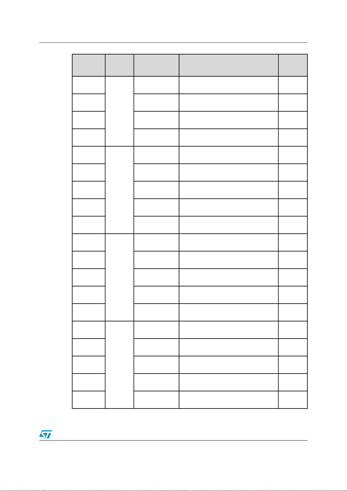
Table 4: Legend/abbreviations for pinout tables
I= Input, O = Output, S = Power supplyType
Output speed
configuration
Reset state
InputLevel
O1 = Slow (up to 2 MHz)
O2 = Fast (up to 10 MHz)
O3 = Fast/slow programmability with slow as default state after reset
O4 = Fast/slow programmability with fast as default state after reset
Output
Bold X (pin state after internal reset release).
Unless otherwise specified, the pin state is the same during the reset
phase and after the internal reset release.
CM = CMOS
HS = High sinkOutput
float = floating, wpu = weak pull-upInputPort and control
T = True open drain, OD = Open drain, PP =
Push pull
19/103DocID022186 Rev 3
44 43 42 41 40 39 38 37
36
35
34
33
32
31
30
29
28
27
26
25
24
23
12
13 14 15 16 17 18
19 20 21 22
1
2
3
4
5
6
7
8
9
10
11
48 47 46 45
(HS) PA6
AIN8/PE7
PC1 (HS)/TIM1_CH1/UART2_CK
PE5/SPI_NSS
PG1
AIN9/PE6
PD3 (HS)/TIM2_CH2 [ADC_ETR]
PD2 (HS)/TIM3_CH1 [TIM2_CH3]
PE0 (HS)/CLK_CCO
PE1 (T)/I
2
C_SCL
PE2 (T)/I
2
C_SDA
PE3/TIM1_BKIN
PD7/TLI [TIM1_CH4]
PD6/UART2_RX
PD5/UART2_TX
PD4 (HS)/TIM2_CH1 [BEEP]
PD1 (HS)/SWIM
PD0 (HS)/TIM3_CH2 [TIM1_BKIN] [CLK_CCO]
V
SSIO_2
PC5 (HS)/SPI_SCK
PC4 (HS)/TIM1_CH4
PC3 (HS)/TIM1_CH3
PC2 (HS)/TIM1_CH2
PG0
PC7 (HS)/SPI_MISO
PC6 (HS)/SPI_MOSI
V
DDIO_2
AIN7/PB7
AIN6/PB6
[I
2
C_SDA] AIN5/PB5
[I
2
C_SCL] AIN4/PB4
[TIM1_ETR/AIN3/PB3
[TIM1_CH3N] AIN2/PB2
[TIM1_CH2N] AIN1/PB1
[TIM1_CH1N] AIN0/PB0
V
DDA
V
SSA
V
SS
VCAP
V
DD
V
DDIO_1
[TIM3_CH1] TIM2_CH3/PA3
(HS) PA4
(HS) PA5
NRST
OSCIN/PA1
OSCOUT/PA2
V
SSIO_1
STM8S005K6 STM8S005C6Pinout and pin description
STM8S005 pinouts and pin description5.1
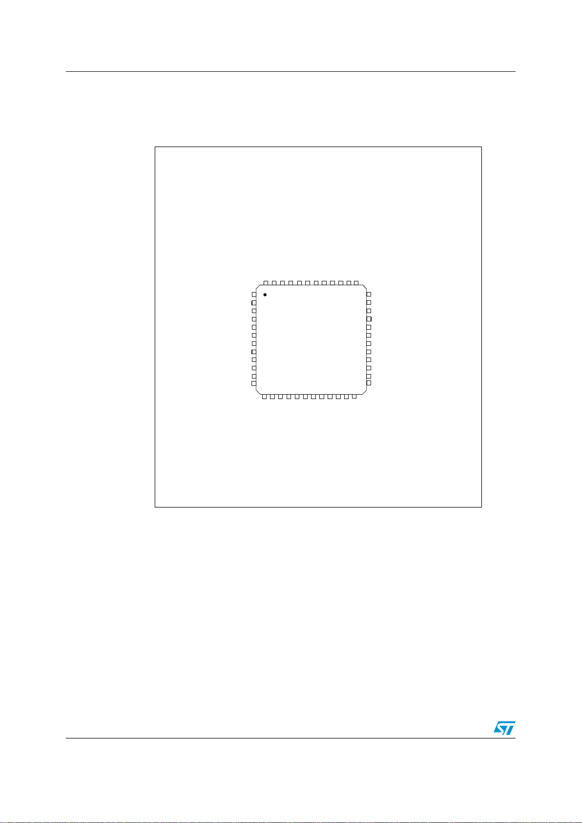
Figure 3: LQFP 48-pin pinout
1. (HS) high sink capability.
2. (T) True open drain (P-buffer and protection diode to VDDnot implemented).
3. [ ] alternate function remapping option (If the same alternate function is shown twice, it
indicates an exclusive choice not a duplication of the function).
DocID022186 Rev 320/103
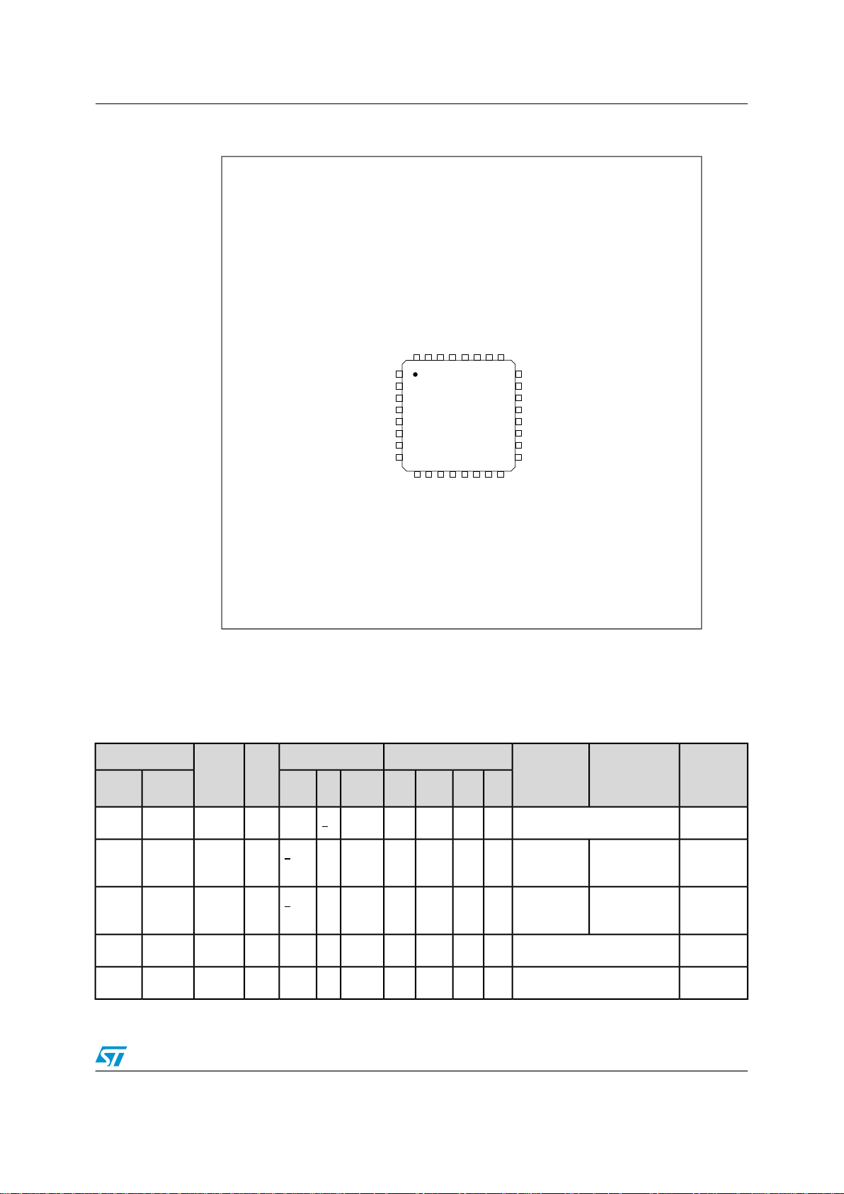
Figure 4: LQFP 32-pin pinout
[I
2
C_SCL] AIN4/PB4
[TIM1_ETR] AIN3/PB3
[TIM1_CH3N] AIN2/PB2
[TIM1_CH2N] AIN1/PB1
[TIM1_CH1N] AIN0/PB0
V
DDA
V
SSA
[I
2
C_SDA] AIN5/PB5
32 31 30 29 28 27 26 25
24
23
22
21
20
19
18
17
9 10 11 12 13 14 15
16
1
2
3
4
5
6
7
8
VCAP
V
DD
V
DDIO
AIN12/PF4
NRST
OSCIN/PA1
OSCOUT/PA2
V
SS
PC3 (HS)/TIM1_CH3
PC2 (HS)/TIM1_CH2
PC1 (HS)/TIM1_CH1/UART2_CK
PE5/SPI_NSS
PC7 (HS)/SPI_MISO
PC6 (HS)/SPI_MOSI
PC5 (HS)/SPI_SCK
PC4 (HS)/TIM1_CH4
PD3 (HS)/TIM2_CH2 [ADC_ETR]
PD2 (HS)/TIM3_CH1[TIM2_CH3]
PD1 (HS)/SWIM
PD0 (HS)/TIM3_CH2 [TIM1_BKIN][CLK_CCO]
PD7/TLI [TIM1_CH4]
PD6/UART2_RX
PD5/UART2_TX
PD4 (HS)/TIM2_CH1 [BEEP]
Pinout and pin descriptionSTM8S005K6 STM8S005C6
22
33
-4
45
1. (HS) high sink capability.
2. [ ] alternate function remapping option (If the same alternate function is shown twice, it
indicates an exclusive choice not a duplication of the function).
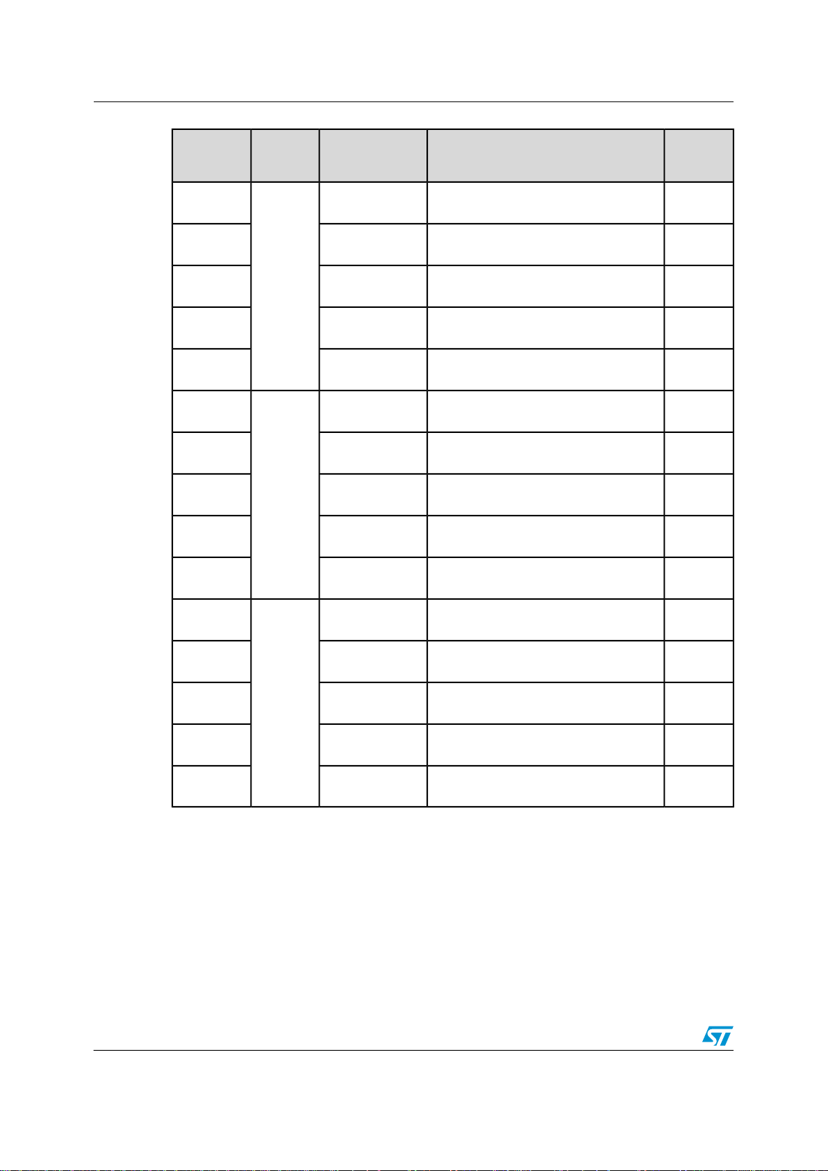
Table 5: Pin description for STM8S005 microcontrollers
Default alternate
function
Resonator/Port A1XXO1XXI/OPA1/ OSC
crystal in
Resonator/Port A2XXO1XXXI/OPA2/ OSC
crystal out
IN
OUT
SSIO_1
SS
wpufloatingLQFP32LQFP48
Ext.
interrupt
OutputInputTypePin namePin number
sink
PPODSpeedHigh
Main function
(after reset)
ResetXI/ONRST11
I/O groundSV
Digital groundSV
Alternate
function after
remap [option
bit]
21/103DocID022186 Rev 3
STM8S005K6 STM8S005C6Pinout and pin description
(2)
Alternate
function after
remap [option
bit]
TIM3_ CH1
[AFR1]
Default alternate
function
Timer 2 -
channel 3
Analog input 12
PPODSpeedHigh
Main function
(after reset)
1.8 V regulator capacitorSVCAP56
Digital power supplySV
I/O power supplySV
Port A3XXO1XXXI/OPA3/ TIM2
Port A4XXO3HSXXXI/OPA4-10
Port A5XXO3HSXXXI/OPA5-11
Port A6XXO3HSXXXI/OPA6-12
Port F4XXO1XXI/OPF4/
Analog power supplySV
Analog groundSV
OutputInputTypePin namePin number
Ext.
wpufloatingLQFP32LQFP48
interrupt
67
78
-9
8-
913
1014
DD
DDIO_1
_CH3
[TIM3
_CH1]
AIN12
DDA
SSA
(1)
sink
Analog input 7Port B7XXO1XXXI/OPB7/ AIN7-15
Analog input 6Port B6XXO1XXXI/OPB6/ AIN6-16
1117
1218
1319
1420
1521
1622
[I2C_
SDA]
[I2C_
SCL]
[TIM1_
ETR]
[TIM1_
CH3N]
[TIM1_
CH2N]
[TIM1_
CH1N]
Analog input 5Port B5XXO1XXXI/OPB5/ AIN5
Analog input 4Port B4XXO1XXXI/OPB4/ AIN4
Analog input 3Port B3XXO1XXXI/OPB3/ AIN3
Analog input 2Port B2XXO1XXXI/OPB2/ AIN2
Analog input 1Port B1XXO1XXXI/OPB1/ AIN1
Analog input 0Port B0XXO1XXXI/OPB0/ AIN0
Analog input 8Port E7XXO1XXXI/OPE7/ AIN8-23
I2C_SDA
[AFR6]
I2C_SCL
[AFR6]
TIM1_ ETR
[AFR5]
TIM1_ CH3N
[AFR5]
TIM1_ CH2N
[AFR5]
TIM1_ CH1N
[AFR5]
Analog input 9Port E6XXO1XXXI/OPE6/ AIN9-24
DocID022186 Rev 322/103
Pinout and pin descriptionSTM8S005K6 STM8S005C6
Default alternate
function
SPI master/slave
select
Timer 1 -Port C1XXO3HSXXXI/OPC1/
channel 1/ UART2
synchronous clock
Timer 1-Port C2XXO3HSXXXI/OPC2/
channel 2
Timer 1 -Port C3XXO3HSXXXI/OPC3/
channel 3
Timer 1 -Port C4XXO3HSXXXI/OPC4/
channel 4
SPI clockPort C5XXO3HSXXXI/OPC5/ SPI_
PPODSpeedHigh
Main function
(after reset)
Port E5XXO1XXXI/OPE5/SPI_
I/O groundSV
I/O power supplySV
OutputInputTypePin namePin number
Ext.
wpufloatingLQFP32LQFP48
interrupt
1725
1826
1927
2028
2129
2230
-31
-32
NSS
TIM1_
CH1/
UART2_CK
TIM1_
CH2
TIM1_
CH3
TIM1_
CH4
SCK
SSIO_2
DDIO_2
sink
Alternate
function after
remap [option
bit]
2333
2434
-37
-38
-39
-40
2541
MOSI
MISO
TIM1_
BKIN
SDA
SCL
CLK_
CCO
TIM3_
CH2
[TIM1_
BKIN]
[CLK_
CCO]
(3)
O1XXI/OPE2/ I2C_
T
(3)
O1XXI/OPE1/ I2C_
T
Port C6XXO3HSXXXI/OPC6/ SPI_
Port C7XXO3HSXXXI/OPC7/ SPI_
Port G0XXO1XXI/OPG0-35
Port G1XXO1XXI/OPG1-36
Port E0XXO3HSXXXI/OPE0/
Port D0XXO3HSXXXI/OPD0/
SPI master out/slave
in
SPI master in/ slave
out
Timer 1 - break inputPort E3XXO1XXXI/OPE3/
I2C dataPort E2
I2C clockPort E1
Configurable clock
output
Timer 3 -
channel 2
TIM1_ BKIN
[AFR3]/ CLK_
CCO [AFR2]
23/103DocID022186 Rev 3
STM8S005K6 STM8S005C6Pinout and pin description
Default alternate
function
SWIM data interfacePort D1XXO4HSXXXI/OPD1/
Timer 3 -
channel 1
Timer 2 -
channel 2
Timer 2 -
channel 1
UART2 data transmitPort D5XXO1XXXI/OPD5/
UART2 data receivePort D6XXO1XXXI/OPD6/
PPODSpeedHigh
Main function
(after reset)
Port D2XXO3HSXXXI/OPD2/
Port D3XXO3HSXXXI/OPD3/
Port D4XXO3HSXXXI/OPD4/
OutputInputTypePin namePin number
Ext.
wpufloatingLQFP32LQFP48
interrupt
2642
2743
2844
2945
3046
3147
SWIM
TIM3_
CH1
[TIM2_
CH3]
TIM2_
CH2
[ADC_
ETR]
TIM2_
CH1
[BEEP]
UART2_
TX
UART2_
RX
(4)
sink
Alternate
function after
remap [option
bit]
TIM2_CH3
[AFR1]
ADC_ ETR
[AFR0]
BEEP output
[AFR7]
3248
(1)
A pull-up is applied to PF4 during the reset phase. This pin is input floating after reset release.
(2)
AIN12 is not selectable in ADC scan mode or with analog watchdog.
(3)
In the open-drain output column, ‘T’ defines a true open-drain I/O (P-buffer, weak pull-up, and protection diode to VDDare not implemented).
(4)
The PD1 pin is in input pull-up during the reset phase and after internal reset release.
[TIM1_
CH4]
Top level interruptPort D7XXO1XXXI/OPD7/ TLI
Alternate function remapping5.1.1
As shown in the rightmost column of the pin description table, some alternate functions can
be remapped at different I/O ports by programming one of eight AFR (alternate function
remap) option bits. When the remapping option is active, the default alternate function is no
longer available.
To use an alternate function, the corresponding peripheral must be enabled in the peripheral
registers.
Alternate function remapping does not effect GPIO capabilities of the I/O ports (see the GPIO
section of the family reference manual, RM0016).
TIM1_ CH4
[AFR4]
DocID022186 Rev 324/103
0x00 FFFF
Flash program memory
(32 Kbytes)
0x00 8000
Reserved
0x01 0000
0x02 7FFF
0x00 0000
RAM
0x00 07FF
(2 Kbytes)
0x00 4000
0x00 407F
128-byte data EEPROM
Reserved
Reserved
0x00 4080
0x00 47FF
32 interrupt vectors
0x00 807F
GPIO and periph. reg.
0x00 5000
0x00 57FF
0x00 5800
0x00 7FFF
0x00 4900
0x00 4FFF
2 Kbytes boot ROM
0x00 6000
0x00 67FF
0x00 6800
0x00 7EFF
CPU/SWIM/debug/ITC
registers
0x00 7F00
0x00 5FFF
Reserved
Reserved
Reserved
Option bytes
0x00 4800
0x00 487F
512 bytes stack
Memory and register mapSTM8S005K6 STM8S005C6
Memory and register map6
Memory map6.1
Figure 5: Memory map
The following table lists the boundary addresses for each memory size. The top of the stack
is at the RAM end address in each case.
25/103DocID022186 Rev 3
STM8S005K6 STM8S005C6Memory and register map
Table 6: Flash, Data EEPROM and RAM boundary addresses
End addressStart addressSize (bytes)Memory area
0x00 FFFF0x00 800032KFlash program memory
0x00 07FF0x00 00002KRAM
0x00 407F0x00 4000128Data EEPROM
Register map6.2
I/O port hardware register map6.2.1
Table 7: I/O port hardware register map
Register nameRegister labelBlockAddress
Port A input pin value registerPA_IDR0x00 5001
Port B input pin value registerPB_IDR0x00 5006
Reset
status
0x00Port A data output latch registerPA_ODRPort A0x00 5000
0xXX
0x00Port A data direction registerPA_DDR0x00 5002
0x00Port A control register 1PA_CR10x00 5003
0x00Port A control register 2PA_CR20x00 5004
0x00Port B data output latch registerPB_ODRPort B0x00 5005
0xXX
0x00Port B data direction registerPB_DDR0x00 5007
0x00Port B control register 1PB_CR10x00 5008
(1)
(1)
0x00Port B control register 2PB_CR20x00 5009
0x00Port C data output latch registerPC_ODRPort C0x00 500A
DocID022186 Rev 326/103
Memory and register mapSTM8S005K6 STM8S005C6
Register nameRegister labelBlockAddress
Reset
status
(1)
Port C input pin value registerPC_IDR0x00 500B
0xXX
0x00Port C data direction registerPC_DDR0x00 500C
0x00Port C control register 1PC_CR10x00 500D
0x00Port C control register 2PC_CR20x00 500E
0x00Port D data output latch registerPD_ODRPort D0x00 500F
(1)
Port D input pin value registerPD_IDR0x00 5010
0xXX
0x00Port D data direction registerPD_DDR0x00 5011
0x02Port D control register 1PD_CR10x00 5012
0x00Port D control register 2PD_CR20x00 5013
0x00Port E data output latch registerPE_ODRPort E0x00 5014
(1)
Port E input pin value registerPE_IDR0x00 5015
0xXX
0x00Port E data direction registerPE_DDR0x00 5016
0x00Port E control register 1PE_CR10x00 5017
0x00Port E control register 2PE_CR20x00 5018
0x00Port F data output latch registerPF_ODRPort F0x00 5019
(1)
Port F input pin value registerPF_IDR0x00 501A
0xXX
0x00Port F data direction registerPF_DDR0x00 501B
0x00Port F control register 1PF_CR10x00 501C
0x00Port F control register 2PF_CR20x00 501D
27/103DocID022186 Rev 3
STM8S005K6 STM8S005C6Memory and register map
Register nameRegister labelBlockAddress
Reset
status
0x00Port G data output latch registerPG_ODRPort G0x00 501E
(1)
Port G input pin value registerPG_IDR0x00 501F
0xXX
0x00Port G data direction registerPG_DDR0x00 5020
0x00Port G control register 1PG_CR10x00 5021
0x00Port G control register 2PG_CR20x00 5022
0x00Port H data output latch registerPH_ODRPort H0x00 5023
(1)
Port H input pin value registerPH_IDR0x00 5024
0xXX
0x00Port H data direction registerPH_DDR0x00 5025
0x00Port H control register 1PH_CR10x00 5026
(1)
Depends on the external circuitry.
0x00Port H control register 2PH_CR20x00 5027
0x00Port I data output latch registerPI_ODRPort I0x00 5028
(1)
Port I input pin value registerPI_IDR0x00 5029
0xXX
0x00Port I data direction registerPI_DDR0x00 502A
0x00Port I control register 1PI_CR10x00 502B
0x00Port I control register 2PI_CR20x00 502C
DocID022186 Rev 328/103
0x00 5059
Memory and register mapSTM8S005K6 STM8S005C6
General hardware register map6.2.2
Table 8: General hardware register map
Reset statusRegister nameRegister labelBlockAddress
Reserved area (10 bytes)0x00 5050 to
0x00 5061
Flash0x00 505A
FLASH_NCR20x00 505C
register 2
FLASH _IAPSR0x00 505F
register
Reserved area (2 bytes)0x00 5060 to
FLASH _PUKRFlash0x00 5062
register
0x00Flash control register 1FLASH_CR1
0x00Flash control register 2FLASH_CR20x00 505B
0xFFFlash complementary control
0x00Flash protection registerFLASH _FPR0x00 505D
0xFFFlash complementary protection registerFLASH _NFPR0x00 505E
0x00Flash in-application programming status
0x00Flash program memory unprotection
0x00 509F
0x00 50B2
Reserved area (1 byte)0x00 5063
0x00Data EEPROM unprotection registerFLASH _DUKRFlash0x00 5064
Reserved area (59 bytes)0x00 5065 to
0x00External interrupt control register 1EXTI_CR1ITC0x00 50A0
0x00External interrupt control register 2EXTI_CR20x00 50A1
Reserved area (17 bytes)0x00 50A2 to
29/103DocID022186 Rev 3
0x00 50BF
STM8S005K6 STM8S005C6Memory and register map
Reset statusRegister nameRegister labelBlockAddress
(1)
Reset status registerRST_SRRST0x00 50B3
0xXX
Reserved area (12 bytes)0x00 50B4 to
0x01Internal clock control registerCLK_ICKRCLK0x00 50C0
0x00External clock control registerCLK_ECKR0x00 50C1
Reserved area (1 byte)0x00 50C2
0xE1Clock master status registerCLK_CMSRCLK0x00 50C3
0xE1Clock master switch registerCLK_SWR0x00 50C4
0x00 50D0
0xXXClock switch control registerCLK_SWCR0x00 50C5
0x18Clock divider registerCLK_CKDIVR0x00 50C6
0xFFPeripheral clock gating register 1CLK_PCKENR10x00 50C7
0x00Clock security system registerCLK_CSSR0x00 50C8
0x00Configurable clock control registerCLK_CCOR0x00 50C9
0xFFPeripheral clock gating register 2CLK_PCKENR20x00 50CA
0x00HSI clock calibration trimming registerCLK_HSITRIMR0x00 50CC
SWIM clock control registerCLK_SWIMCCR0x00 50CD
0bXXXX
XXX0
Reserved area (3 bytes)0x00 50CE to
0x7FWWDG control registerWWDG_CRWWDG0x00 50D1
0x7FWWDR window registerWWDG_WR0x00 50D2
DocID022186 Rev 330/103
 Loading...