

STM8L151C2/K2/G2/F2
UFQFPN28
UFQFPN32
TSSOP20
UFQFPN20
LQFP48
STM8L151C3/K3/G3/F3
8-bit ultralow power MCU, up to 8 KB Flash, up to 256 B data EEPROM,
RTC, timers, USART, I2C, SPI, ADC, comparators
Datasheet − production data
Features
■ Operating conditions
– Operating power supply: 1.65 to 3.6 V
(without BOR), 1.8 to 3.6 V (with BOR)
– Temperature range: -40 to 85 or 125 °C
■ Low power features
– 5 low power modes: Wait, Low power run,
Low power wait, Active-halt with RTC, Halt
– Ultralow leakage per I/0: 50 nA
– Fast wakeup from Halt: 5 µs
■ Advanced STM8 core
– Harvard architecture and 3-stage pipeline
– Max freq: 16 MHz, 16 CISC MIPS peak
– Up to 40 external interrupt sources
■ Reset and supply management
– Low power, ultrasafe BOR reset with 5
selectable thresholds
– Ultralow power POR/PDR
– Programmable voltage detector (PVD)
■ Clock management
– 32 kHz and 1-16 MHz crystal oscillators
– Internal 16 MHz factory-trimmed RC
– Internal 38 kHz low consumption RC
– Clock security system
■ Low power RTC
– BCD calendar with alarm interrupt
– Digital calibration with +/- 0.5 ppm accuracy
– LSE security system
– Auto-wakeup from Halt w/ periodic interrupt
■ Memories
– Up to 8 Kbytes of Flash program memory
plus 256 bytes of data EEPROM with ECC
– Flexible write/read protection modes
– 1 Kbyte of RAM
■ DMA
– 4 channels supporting ADC, SPI, I
2
USART, timers
– 1 channel for memory-to-memory
■ 12-bit ADC up to 1 Msps/28 channels
– Temp. sensor and internal ref. voltage
■ 2 ultralow power comparators
– 1 with fixed threshold and 1 rail to rail
– Wakeup capability
■ Timers
– Two 16-bit timers with 2 channels (IC, OC,
PWM), quadrature encoder (TIM2, TIM3)
– One 8-bit timer with 7-bit prescaler (TIM4)
– 1 Window and 1 independent watchdog
– Beeper timer with 1, 2 or 4 kHz frequencies
■ Communication interfaces
– One synchronous serial interface (SPI)
–Fast I
2
C 400 kHz
– One USART
■ Up to 41 I/Os, all mappable on interrupt vectors
■ Up to 20 capacitive sensing channels
supporting touchkey, proximity touch, linear
touch, and rotary touch sensors
■ Development support
– Fast on-chip programming and non-
intrusive debugging with SWIM
– Bootloader using USART
■ 96-bit unique ID
C,
July 2012 Doc ID 018780 Rev 4 1/112
www.st.comThis is information on a product in full production.
1

Contents STM8L151x2, STM8L151x3
Contents
1 Introduction . . . . . . . . . . . . . . . . . . . . . . . . . . . . . . . . . . . . . . . . . . . . . . . . 9
2 Description . . . . . . . . . . . . . . . . . . . . . . . . . . . . . . . . . . . . . . . . . . . . . . . . 11
2.1 Device overview . . . . . . . . . . . . . . . . . . . . . . . . . . . . . . . . . . . . . . . . . . . . 12
2.2 Ultra-low-power continuum . . . . . . . . . . . . . . . . . . . . . . . . . . . . . . . . . . . . 13
3 Functional overview . . . . . . . . . . . . . . . . . . . . . . . . . . . . . . . . . . . . . . . . 14
3.1 Low power modes . . . . . . . . . . . . . . . . . . . . . . . . . . . . . . . . . . . . . . . . . . 15
3.2 Central processing unit STM8 . . . . . . . . . . . . . . . . . . . . . . . . . . . . . . . . . 15
3.2.1 Advanced STM8 Core . . . . . . . . . . . . . . . . . . . . . . . . . . . . . . . . . . . . . . 15
3.2.2 Interrupt controller . . . . . . . . . . . . . . . . . . . . . . . . . . . . . . . . . . . . . . . . . 16
3.3 Reset and supply management . . . . . . . . . . . . . . . . . . . . . . . . . . . . . . . . 17
3.3.1 Power supply scheme . . . . . . . . . . . . . . . . . . . . . . . . . . . . . . . . . . . . . . 17
3.3.2 Power supply supervisor . . . . . . . . . . . . . . . . . . . . . . . . . . . . . . . . . . . . 17
3.3.3 Voltage regulator . . . . . . . . . . . . . . . . . . . . . . . . . . . . . . . . . . . . . . . . . . 17
3.4 Clock management . . . . . . . . . . . . . . . . . . . . . . . . . . . . . . . . . . . . . . . . . 18
3.5 Low power real-time clock . . . . . . . . . . . . . . . . . . . . . . . . . . . . . . . . . . . . 19
3.6 Memories . . . . . . . . . . . . . . . . . . . . . . . . . . . . . . . . . . . . . . . . . . . . . . . . . 20
3.7 DMA . . . . . . . . . . . . . . . . . . . . . . . . . . . . . . . . . . . . . . . . . . . . . . . . . . . . . 20
3.8 Analog-to-digital converter . . . . . . . . . . . . . . . . . . . . . . . . . . . . . . . . . . . . 20
3.9 Ultra-low-power comparators . . . . . . . . . . . . . . . . . . . . . . . . . . . . . . . . . . 20
3.10 System configuration controller and routing interface . . . . . . . . . . . . . . . 21
3.11 Touchsensing . . . . . . . . . . . . . . . . . . . . . . . . . . . . . . . . . . . . . . . . . . . . . . 21
3.12 Timers . . . . . . . . . . . . . . . . . . . . . . . . . . . . . . . . . . . . . . . . . . . . . . . . . . . 21
3.12.1 16-bit general purpose timers . . . . . . . . . . . . . . . . . . . . . . . . . . . . . . . . 22
3.12.2 8-bit basic timer . . . . . . . . . . . . . . . . . . . . . . . . . . . . . . . . . . . . . . . . . . . 22
3.13 Watchdog timers . . . . . . . . . . . . . . . . . . . . . . . . . . . . . . . . . . . . . . . . . . . 22
3.13.1 Window watchdog timer . . . . . . . . . . . . . . . . . . . . . . . . . . . . . . . . . . . . . 22
3.13.2 Independent watchdog timer . . . . . . . . . . . . . . . . . . . . . . . . . . . . . . . . . 22
3.14 Beeper . . . . . . . . . . . . . . . . . . . . . . . . . . . . . . . . . . . . . . . . . . . . . . . . . . . 22
3.15 Communication interfaces . . . . . . . . . . . . . . . . . . . . . . . . . . . . . . . . . . . . 23
3.15.1 SPI . . . . . . . . . . . . . . . . . . . . . . . . . . . . . . . . . . . . . . . . . . . . . . . . . . . . . 23
2/112 Doc ID 018780 Rev 4

STM8L151x2, STM8L151x3 Contents
3.15.2 I²C . . . . . . . . . . . . . . . . . . . . . . . . . . . . . . . . . . . . . . . . . . . . . . . . . . . . . 23
3.15.3 USART . . . . . . . . . . . . . . . . . . . . . . . . . . . . . . . . . . . . . . . . . . . . . . . . . . 23
3.16 Infrared (IR) interface . . . . . . . . . . . . . . . . . . . . . . . . . . . . . . . . . . . . . . . . 23
3.17 Development support . . . . . . . . . . . . . . . . . . . . . . . . . . . . . . . . . . . . . . . . 24
4 Pin description . . . . . . . . . . . . . . . . . . . . . . . . . . . . . . . . . . . . . . . . . . . . 25
4.1 System configuration options . . . . . . . . . . . . . . . . . . . . . . . . . . . . . . . . . . 30
5 Memory and register map . . . . . . . . . . . . . . . . . . . . . . . . . . . . . . . . . . . 31
5.1 Memory mapping . . . . . . . . . . . . . . . . . . . . . . . . . . . . . . . . . . . . . . . . . . . 31
5.2 Register map . . . . . . . . . . . . . . . . . . . . . . . . . . . . . . . . . . . . . . . . . . . . . . 32
6 Interrupt vector mapping . . . . . . . . . . . . . . . . . . . . . . . . . . . . . . . . . . . . 47
7 Electrical parameters . . . . . . . . . . . . . . . . . . . . . . . . . . . . . . . . . . . . . . . 49
7.1 Parameter conditions . . . . . . . . . . . . . . . . . . . . . . . . . . . . . . . . . . . . . . . . 49
7.1.1 Minimum and maximum values . . . . . . . . . . . . . . . . . . . . . . . . . . . . . . . 49
7.1.2 Typical values . . . . . . . . . . . . . . . . . . . . . . . . . . . . . . . . . . . . . . . . . . . . . 49
7.1.3 Typical curves . . . . . . . . . . . . . . . . . . . . . . . . . . . . . . . . . . . . . . . . . . . . 49
7.1.4 Loading capacitor . . . . . . . . . . . . . . . . . . . . . . . . . . . . . . . . . . . . . . . . . 49
7.1.5 Pin input voltage . . . . . . . . . . . . . . . . . . . . . . . . . . . . . . . . . . . . . . . . . . 50
7.2 Absolute maximum ratings . . . . . . . . . . . . . . . . . . . . . . . . . . . . . . . . . . . . 50
7.3 Operating conditions . . . . . . . . . . . . . . . . . . . . . . . . . . . . . . . . . . . . . . . . 52
7.3.1 General operating conditions . . . . . . . . . . . . . . . . . . . . . . . . . . . . . . . . . 52
7.3.2 Embedded reset and power control block characteristics . . . . . . . . . . . 53
7.3.3 Supply current characteristics . . . . . . . . . . . . . . . . . . . . . . . . . . . . . . . . 54
7.3.4 Clock and timing characteristics . . . . . . . . . . . . . . . . . . . . . . . . . . . . . . 65
7.3.5 Memory characteristics . . . . . . . . . . . . . . . . . . . . . . . . . . . . . . . . . . . . . 71
7.3.6 I/O current injection characteristics . . . . . . . . . . . . . . . . . . . . . . . . . . . . 72
7.3.7 I/O port pin characteristics . . . . . . . . . . . . . . . . . . . . . . . . . . . . . . . . . . . 72
7.3.8 Communication interfaces . . . . . . . . . . . . . . . . . . . . . . . . . . . . . . . . . . . 80
7.3.9 Embedded reference voltage . . . . . . . . . . . . . . . . . . . . . . . . . . . . . . . . . 85
7.3.10 Temperature sensor . . . . . . . . . . . . . . . . . . . . . . . . . . . . . . . . . . . . . . . . 86
7.3.11 Comparator characteristics . . . . . . . . . . . . . . . . . . . . . . . . . . . . . . . . . . 86
7.3.12 12-bit ADC1 characteristics . . . . . . . . . . . . . . . . . . . . . . . . . . . . . . . . . . 88
7.3.13 EMC characteristics . . . . . . . . . . . . . . . . . . . . . . . . . . . . . . . . . . . . . . . . 93
Doc ID 018780 Rev 4 3/112

Contents STM8L151x2, STM8L151x3
7.4 Thermal characteristics . . . . . . . . . . . . . . . . . . . . . . . . . . . . . . . . . . . . . . 96
8 Option bytes . . . . . . . . . . . . . . . . . . . . . . . . . . . . . . . . . . . . . . . . . . . . . . 97
9 Unique ID . . . . . . . . . . . . . . . . . . . . . . . . . . . . . . . . . . . . . . . . . . . . . . . . 100
10 Package characteristics . . . . . . . . . . . . . . . . . . . . . . . . . . . . . . . . . . . . 101
10.1 ECOPACK . . . . . . . . . . . . . . . . . . . . . . . . . . . . . . . . . . . . . . . . . . . . . . . 101
10.2 Package mechanical data . . . . . . . . . . . . . . . . . . . . . . . . . . . . . . . . . . . 102
10.2.1 48-pin low profile quad flat 7x7mm package (LQFP48) . . . . . . . . . . . . 102
10.2.2 32-lead ultra thin fine pitch quad flat no-lead 5x5 mm package
(UFQFPN32) . . . . . . . . . . . . . . . . . . . . . . . . . . . . . . . . . . . . . . . . . . . . 103
10.2.3 28-lead ultra thin fine pitch quad flat no-lead 4x4 mm package
(UFQFPN28) . . . . . . . . . . . . . . . . . . . . . . . . . . . . . . . . . . . . . . . . . . . . 105
10.2.4 20-lead ultra thin fine pitch quad flat no-lead package (UFQFPN20) . 107
11 Device ordering information . . . . . . . . . . . . . . . . . . . . . . . . . . . . . . . . . 110
12 Revision history . . . . . . . . . . . . . . . . . . . . . . . . . . . . . . . . . . . . . . . . . . 111
4/112 Doc ID 018780 Rev 4

STM8L151x2, STM8L151x3 List of tables
List of tables
Table 1. Low density STM8L15xxx low power device features and peripheral counts. . . . . . . . . . . 12
Table 2. Timer feature comparison . . . . . . . . . . . . . . . . . . . . . . . . . . . . . . . . . . . . . . . . . . . . . . . . . . 21
Table 3. Legend/abbreviation for table 4 . . . . . . . . . . . . . . . . . . . . . . . . . . . . . . . . . . . . . . . . . . . . . 27
Table 4. Low density STM8L15xxx pin description. . . . . . . . . . . . . . . . . . . . . . . . . . . . . . . . . . . . . . 27
Table 5. Flash and RAM boundary addresses . . . . . . . . . . . . . . . . . . . . . . . . . . . . . . . . . . . . . . . . . 32
Table 6. Factory conversion registers. . . . . . . . . . . . . . . . . . . . . . . . . . . . . . . . . . . . . . . . . . . . . . . . 32
Table 7. I/O port hardware register map . . . . . . . . . . . . . . . . . . . . . . . . . . . . . . . . . . . . . . . . . . . . . . 32
Table 8. General hardware register map . . . . . . . . . . . . . . . . . . . . . . . . . . . . . . . . . . . . . . . . . . . . . 33
Table 9. CPU/SWIM/debug module/interrupt controller registers. . . . . . . . . . . . . . . . . . . . . . . . . . . 45
Table 10. Interrupt mapping . . . . . . . . . . . . . . . . . . . . . . . . . . . . . . . . . . . . . . . . . . . . . . . . . . . . . . . . 47
Table 11. Voltage characteristics . . . . . . . . . . . . . . . . . . . . . . . . . . . . . . . . . . . . . . . . . . . . . . . . . . . . 50
Table 12. Current characteristics . . . . . . . . . . . . . . . . . . . . . . . . . . . . . . . . . . . . . . . . . . . . . . . . . . . . 51
Table 13. Thermal characteristics. . . . . . . . . . . . . . . . . . . . . . . . . . . . . . . . . . . . . . . . . . . . . . . . . . . . 51
Table 14. General operating conditions . . . . . . . . . . . . . . . . . . . . . . . . . . . . . . . . . . . . . . . . . . . . . . . 52
Table 15. Embedded reset and power control block characteristics. . . . . . . . . . . . . . . . . . . . . . . . . . 53
Table 16. Total current consumption in Run mode . . . . . . . . . . . . . . . . . . . . . . . . . . . . . . . . . . . . . . . 55
Table 17. Total current consumption in Wait mode . . . . . . . . . . . . . . . . . . . . . . . . . . . . . . . . . . . . . . 57
Table 18. Total current consumption and timing in Low power run mode at VDD = 1.65 V to
3.6 V . . . . . . . . . . . . . . . . . . . . . . . . . . . . . . . . . . . . . . . . . . . . . . . . . . . . . . . . . . . . . . . . . 59
Table 19. Total current consumption in Low power wait mode at VDD = 1.65 V to 3.6 V . . . . . . . . . 61
Table 20. Total current consumption and timing in Active-halt mode at VDD = 1.65 V to 3.6 V. . . . . 62
Table 21. Typical current consumption in Active-halt mode, RTC clocked by LSE external crystal. . 62
Table 22. Total current consumption and timing in Halt mode at VDD = 1.65 to 3.6 V . . . . . . . . . . . 63
Table 23. Peripheral current consumption . . . . . . . . . . . . . . . . . . . . . . . . . . . . . . . . . . . . . . . . . . . . . 64
Table 24. Current consumption under external reset . . . . . . . . . . . . . . . . . . . . . . . . . . . . . . . . . . . . . 65
Table 25. HSE external clock characteristics . . . . . . . . . . . . . . . . . . . . . . . . . . . . . . . . . . . . . . . . . . . 65
Table 26. LSE external clock characteristics . . . . . . . . . . . . . . . . . . . . . . . . . . . . . . . . . . . . . . . . . . . 65
Table 27. HSE oscillator characteristics . . . . . . . . . . . . . . . . . . . . . . . . . . . . . . . . . . . . . . . . . . . . . . . 66
Table 28. LSE oscillator characteristics . . . . . . . . . . . . . . . . . . . . . . . . . . . . . . . . . . . . . . . . . . . . . . . 67
Table 29. HSI oscillator characteristics. . . . . . . . . . . . . . . . . . . . . . . . . . . . . . . . . . . . . . . . . . . . . . . . 68
Table 30. LSI oscillator characteristics . . . . . . . . . . . . . . . . . . . . . . . . . . . . . . . . . . . . . . . . . . . . . . . . 69
Table 31. RAM and hardware registers . . . . . . . . . . . . . . . . . . . . . . . . . . . . . . . . . . . . . . . . . . . . . . . 71
Table 32. Flash program and data EEPROM memory . . . . . . . . . . . . . . . . . . . . . . . . . . . . . . . . . . . . 71
Table 33. I/O current injection susceptibility . . . . . . . . . . . . . . . . . . . . . . . . . . . . . . . . . . . . . . . . . . . . 72
Table 34. I/O static characteristics . . . . . . . . . . . . . . . . . . . . . . . . . . . . . . . . . . . . . . . . . . . . . . . . . . . 73
Table 35. Output driving current (high sink ports). . . . . . . . . . . . . . . . . . . . . . . . . . . . . . . . . . . . . . . . 76
Table 36. Output driving current (true open drain ports) . . . . . . . . . . . . . . . . . . . . . . . . . . . . . . . . . . . 76
Table 37. Output driving current (PA0 with high sink LED driver capability). . . . . . . . . . . . . . . . . . . . 76
Table 38. NRST pin characteristics . . . . . . . . . . . . . . . . . . . . . . . . . . . . . . . . . . . . . . . . . . . . . . . . . . 78
Table 39. SPI1 characteristics . . . . . . . . . . . . . . . . . . . . . . . . . . . . . . . . . . . . . . . . . . . . . . . . . . . . . . 80
Table 40. I2C characteristics . . . . . . . . . . . . . . . . . . . . . . . . . . . . . . . . . . . . . . . . . . . . . . . . . . . . . . . 83
Table 41. Reference voltage characteristics. . . . . . . . . . . . . . . . . . . . . . . . . . . . . . . . . . . . . . . . . . . . 85
Table 42. TS characteristics . . . . . . . . . . . . . . . . . . . . . . . . . . . . . . . . . . . . . . . . . . . . . . . . . . . . . . . . 86
Table 43. Comparator 1 characteristics . . . . . . . . . . . . . . . . . . . . . . . . . . . . . . . . . . . . . . . . . . . . . . . 86
Table 44. Comparator 2 characteristics . . . . . . . . . . . . . . . . . . . . . . . . . . . . . . . . . . . . . . . . . . . . . . . 87
Table 45. ADC1 characteristics . . . . . . . . . . . . . . . . . . . . . . . . . . . . . . . . . . . . . . . . . . . . . . . . . . . . . 88
Table 46. ADC1 accuracy with VDDA = 3.3 V to 2.5 V. . . . . . . . . . . . . . . . . . . . . . . . . . . . . . . . . . . . 90
Table 47. ADC1 accuracy with VDDA = 2.4 V to 3.6 V. . . . . . . . . . . . . . . . . . . . . . . . . . . . . . . . . . . . 90
Doc ID 018780 Rev 4 5/112

List of tables STM8L151x2, STM8L151x3
Table 48. ADC1 accuracy with VDDA = VREF+ = 1.8 V to 2.4 V . . . . . . . . . . . . . . . . . . . . . . . . . . . . 90
Table 49. R
max for f
AIN
= 16 MHz . . . . . . . . . . . . . . . . . . . . . . . . . . . . . . . . . . . . . . . . . . . . . . . . 93
ADC
Table 50. EMS data . . . . . . . . . . . . . . . . . . . . . . . . . . . . . . . . . . . . . . . . . . . . . . . . . . . . . . . . . . . . . . 94
Table 51. EMI data . . . . . . . . . . . . . . . . . . . . . . . . . . . . . . . . . . . . . . . . . . . . . . . . . . . . . . . . . . . . . . 94
Table 52. ESD absolute maximum ratings . . . . . . . . . . . . . . . . . . . . . . . . . . . . . . . . . . . . . . . . . . . . . 95
Table 53. Electrical sensitivities . . . . . . . . . . . . . . . . . . . . . . . . . . . . . . . . . . . . . . . . . . . . . . . . . . . . . 95
Table 54. Thermal characteristics. . . . . . . . . . . . . . . . . . . . . . . . . . . . . . . . . . . . . . . . . . . . . . . . . . . . 96
Table 55. Option byte addresses . . . . . . . . . . . . . . . . . . . . . . . . . . . . . . . . . . . . . . . . . . . . . . . . . . . . 97
Table 56. Option byte description . . . . . . . . . . . . . . . . . . . . . . . . . . . . . . . . . . . . . . . . . . . . . . . . . . . . 98
Table 57. Unique ID registers (96 bits) . . . . . . . . . . . . . . . . . . . . . . . . . . . . . . . . . . . . . . . . . . . . . . . 100
Table 58. LQFP48 package mechanical data. . . . . . . . . . . . . . . . . . . . . . . . . . . . . . . . . . . . . . . . . . 102
Table 59. UFQFPN32 package mechanical data . . . . . . . . . . . . . . . . . . . . . . . . . . . . . . . . . . . . . . . 104
Table 60. UFQFPN28 package mechanical data . . . . . . . . . . . . . . . . . . . . . . . . . . . . . . . . . . . . . . . 105
Table 61. UFQFPN20 - 20-lead ultra thin fine pitch quad flat package (3x3)
package mechanical data . . . . . . . . . . . . . . . . . . . . . . . . . . . . . . . . . . . . . . . . . . . . . . . . 108
Table 62. TSSOP20 - 20-pin thin shrink small outline package mechanical data . . . . . . . . . . . . . . 109
6/112 Doc ID 018780 Rev 4

STM8L151x2, STM8L151x3 List of figures
List of figures
Figure 1. Low density STM8L151xx device block diagram . . . . . . . . . . . . . . . . . . . . . . . . . . . . . . . . 14
Figure 2. Low density STM8L15x clock tree diagram . . . . . . . . . . . . . . . . . . . . . . . . . . . . . . . . . . . . 19
Figure 3. STM8L151Cx LQFP48 package pinout . . . . . . . . . . . . . . . . . . . . . . . . . . . . . . . . . . . . . . . 25
Figure 4. STM8L151Kx UFQFPN32 package pinout . . . . . . . . . . . . . . . . . . . . . . . . . . . . . . . . . . . . . 25
Figure 5. STM8L151Gx UFQFPN28 package pinout . . . . . . . . . . . . . . . . . . . . . . . . . . . . . . . . . . . . 25
Figure 6. STM8L151Fx UFQFPN20 package pinout . . . . . . . . . . . . . . . . . . . . . . . . . . . . . . . . . . . . . 26
Figure 7. STM8L151Fx TSSOP20 package pinout . . . . . . . . . . . . . . . . . . . . . . . . . . . . . . . . . . . . . . 26
Figure 8. Memory map . . . . . . . . . . . . . . . . . . . . . . . . . . . . . . . . . . . . . . . . . . . . . . . . . . . . . . . . . . . 31
Figure 9. Pin loading conditions . . . . . . . . . . . . . . . . . . . . . . . . . . . . . . . . . . . . . . . . . . . . . . . . . . . . . 49
Figure 10. Pin input voltage . . . . . . . . . . . . . . . . . . . . . . . . . . . . . . . . . . . . . . . . . . . . . . . . . . . . . . . . . 50
Figure 11. POR/BOR thresholds . . . . . . . . . . . . . . . . . . . . . . . . . . . . . . . . . . . . . . . . . . . . . . . . . . . . . 54
Figure 12. Typ. IDD(RUN) vs. VDD, fCPU = 16 MHz . . . . . . . . . . . . . . . . . . . . . . . . . . . . . . . . . . . . . 56
Figure 13. Typ. IDD(Wait) vs. VDD, fCPU = 16 MHz 1). . . . . . . . . . . . . . . . . . . . . . . . . . . . . . . . . . . . 58
Figure 14. Typ. IDD(LPR) vs. VDD (LSI clock source) . . . . . . . . . . . . . . . . . . . . . . . . . . . . . . . . . . . . 60
Figure 15. Typ. IDD(LPW) vs. VDD (LSI clock source) . . . . . . . . . . . . . . . . . . . . . . . . . . . . . . . . . . . . 61
Figure 16. HSE oscillator circuit diagram. . . . . . . . . . . . . . . . . . . . . . . . . . . . . . . . . . . . . . . . . . . . . . . 66
Figure 17. LSE oscillator circuit diagram . . . . . . . . . . . . . . . . . . . . . . . . . . . . . . . . . . . . . . . . . . . . . . . 67
Figure 18. Typical HSI frequency vs V
Figure 19. Typical LSI frequency vs. VDD . . . . . . . . . . . . . . . . . . . . . . . . . . . . . . . . . . . . . . . . . . . . . 70
Figure 20. Typical VIL and VIH vs VDD (high sink I/Os) . . . . . . . . . . . . . . . . . . . . . . . . . . . . . . . . . . . 74
Figure 21. Typical VIL and VIH vs VDD (true open drain I/Os) . . . . . . . . . . . . . . . . . . . . . . . . . . . . . . 74
Figure 22. Typical pull-up resistance R
Figure 23. Typical pull-up current I
Figure 24. Typ. VOL @ VDD = 3.0 V (high sink ports) . . . . . . . . . . . . . . . . . . . . . . . . . . . . . . . . . . . . 77
Figure 25. Typ. VOL @ VDD = 1.8 V (high sink ports) . . . . . . . . . . . . . . . . . . . . . . . . . . . . . . . . . . . . 77
Figure 26. Typ. VOL @ VDD = 3.0 V (true open drain ports) . . . . . . . . . . . . . . . . . . . . . . . . . . . . . . . 77
Figure 27. Typ. VOL @ VDD = 1.8 V (true open drain ports) . . . . . . . . . . . . . . . . . . . . . . . . . . . . . . . 77
Figure 28. Typ. VDD - VOH @ VDD = 3.0 V (high sink ports) . . . . . . . . . . . . . . . . . . . . . . . . . . . . . . . 77
Figure 29. Typ. VDD - VOH @ VDD = 1.8 V (high sink ports) . . . . . . . . . . . . . . . . . . . . . . . . . . . . . . . 77
Figure 30. Typical NRST pull-up resistance R
Figure 31. Typical NRST pull-up current I
Figure 32. Recommended NRST pin configuration . . . . . . . . . . . . . . . . . . . . . . . . . . . . . . . . . . . . . . . 79
Figure 33. SPI1 timing diagram - slave mode and CPHA=0 . . . . . . . . . . . . . . . . . . . . . . . . . . . . . . . . 81
Figure 34. SPI1 timing diagram - slave mode and CPHA=1
Figure 35. SPI1 timing diagram - master mode
Figure 36. Typical application with I2C bus and timing diagram 1) . . . . . . . . . . . . . . . . . . . . . . . . . . . 84
Figure 37. ADC1 accuracy characteristics . . . . . . . . . . . . . . . . . . . . . . . . . . . . . . . . . . . . . . . . . . . . . . 91
Figure 38. Typical connection diagram using the ADC1 . . . . . . . . . . . . . . . . . . . . . . . . . . . . . . . . . . . 91
Figure 39. Power supply and reference decoupling (V
Figure 40. Power supply and reference decoupling (VREF+ connected to VDDA) . . . . . . . . . . . . . . . 92
Figure 41. Max. dynamic current consumption on V
conversion . . . . . . . . . . . . . . . . . . . . . . . . . . . . . . . . . . . . . . . . . . . . . . . . . . . . . . . . . . . . . 93
Figure 42. LQFP48 package outline . . . . . . . . . . . . . . . . . . . . . . . . . . . . . . . . . . . . . . . . . . . . . . . . . 102
Figure 43. UFQFPN32 package outline . . . . . . . . . . . . . . . . . . . . . . . . . . . . . . . . . . . . . . . . . . . . . . . 103
Figure 44. Recommended UFQFPN32 footprint . . . . . . . . . . . . . . . . . . . . . . . . . . . . . . . . . . . . . . . . 104
Figure 45. UFQFPN28 package outline . . . . . . . . . . . . . . . . . . . . . . . . . . . . . . . . . . . . . . . . . . . . . . . 105
Figure 46. Recommended UFQFPN28 footprint (dimensions in mm) . . . . . . . . . . . . . . . . . . . . . . . . 106
Figure 47. UFQFPN20 - 20-lead ultra thin fine pitch quad flat package outline (3x3) . . . . . . . . . . . . 107
. . . . . . . . . . . . . . . . . . . . . . . . . . . . . . . . . . . . . . . . . . . . . . . 69
DD
vs VDD with VIN=VSS . . . . . . . . . . . . . . . . . . . . . . . . . . . . 75
PU
vs VDD with VIN=VSS . . . . . . . . . . . . . . . . . . . . . . . . . . . . . . . . 75
pu
vs VDD . . . . . . . . . . . . . . . . . . . . . . . . . . . . . . . . . . 78
PU
vs VDD . . . . . . . . . . . . . . . . . . . . . . . . . . . . . . . . . . . . . . 79
pu
(1)
(1)
. . . . . . . . . . . . . . . . . . . . . . . . . . . . . . . . . . . . . . . . 82
REF+
REF+
. . . . . . . . . . . . . . . . . . . . . . . . . . . . . . 81
not connected to V
). . . . . . . . . . . . . . 92
DDA
supply pin during ADC
Doc ID 018780 Rev 4 7/112

List of figures STM8L151x2, STM8L151x3
Figure 48. UFQFPN20 recommended footprint (dimensions in mm). . . . . . . . . . . . . . . . . . . . . . . . . 107
Figure 49. TSSOP20 - 20-pin thin shrink small outline package . . . . . . . . . . . . . . . . . . . . . . . . . . . . 109
Figure 50. Low density STM8L15xxx ordering information scheme . . . . . . . . . . . . . . . . . . . . . . . . . 110
8/112 Doc ID 018780 Rev 4

STM8L151x2, STM8L151x3 Introduction
1 Introduction
This document describes the features, pinout, mechanical data and ordering information for
the Low density STM8L15xxx devices: STM8L151x2 and STM8L151x3 microcontrollers
with a Flash memory density of up to 8 Kbytes.
For further details on the STMicroelectronics Ultralow power family please refer to
Section 2.2: Ultra-low-power continuum on page 13.
For detailed information on device operation and registers, refer to the reference manual
(RM0031).
For information on to the Flash program memory and data EEPROM, refer to the
programming manual (PM0054).
For information on the debug module and SWIM (single wire interface module), refer to the
STM8 SWIM communication protocol and debug module user manual (UM0470).
For information on the STM8 core, refer to the STM8 CPU programming manual (PM0044).
Low density devices provide the following benefits:
● Integrated system
– Up to 8 Kbytes of low-density embedded Flash program memory
– 256 bytes of data EEPROM
– 1 Kbyte of RAM
– Internal high-speed and low-power low speed RC.
– Embedded reset
● Ultralow power consumption
– 1 µA in Active-halt mode
– Clock gated system and optimized power management
– Capability to execute from RAM for Low power wait mode and Low power run
mode
● Advanced features
– Up to 16 MIPS at 16 MHz CPU clock frequency
– Direct memory access (DMA) for memory-to-memory or peripheral-to-memory
access.
● Short development cycles
– Application scalability across a common family product architecture with
compatible pinout, memory map and modular peripherals.
– Wide choice of development tools
Doc ID 018780 Rev 4 9/112

Introduction STM8L151x2, STM8L151x3
STM8L Ultralow power microcontrollers can operate either from 1.8 to 3.6 V (down to 1.65 V
at power-down) or from 1.65 to 3.6 V. They are available in the -40 to +85 °C and -40 to
+125 °C temperature ranges.
These features make the STM8L Ultralow power microcontroller families suitable for a wide
range of applications:
● Medical and handheld equipment
● Application control and user interface
● PC peripherals, gaming, GPS and sport equipment
● Alarm systems, wired and wireless sensors
● Metering
The devices are offered in five different packages from 20 to 48 pins. Different sets of
peripherals are included depending on the device. Refer to Section 3 for an overview of the
complete range of peripherals proposed in this family.
All STM8L Ultralow power products are based on the same architecture with the same
memory mapping and a coherent pinout.
Figure 1 shows the block diagram of the STM8L Low density family.
10/112 Doc ID 018780 Rev 4

STM8L151x2, STM8L151x3 Description
2 Description
The Low density STM8L15xxx Ultralow power devices feature an enhanced STM8 CPU
core providing increased processing power (up to 16 MIPS at 16 MHz) while maintaining the
advantages of a CISC architecture with improved code density, a 24-bit linear addressing
space and an optimized architecture for low power operations.
The family includes an integrated debug module with a hardware interface (SWIM) which
allows non-intrusive in-application debugging and ultrafast Flash programming.
All Low density STM8L15xxx microcontrollers feature embedded data EEPROM and low
power low-voltage single-supply program Flash memory.
The devices incorporate an extensive range of enhanced I/Os and peripherals, a 12-bit
ADC, two comparators, a real-time clock, two 16-bit timers, one 8-bit timer, as well as
standard communication interfaces such as an SPI, an I
modular design of the peripheral set allows the same peripherals to be found in different ST
microcontroller families including 32-bit families. This makes any transition to a different
family very easy, and simplified even more by the use of a common set of development
tools.
2
C interface, and one USART. The
Doc ID 018780 Rev 4 11/112
Description STM8L151x2, STM8L151x3
2.1 Device overview
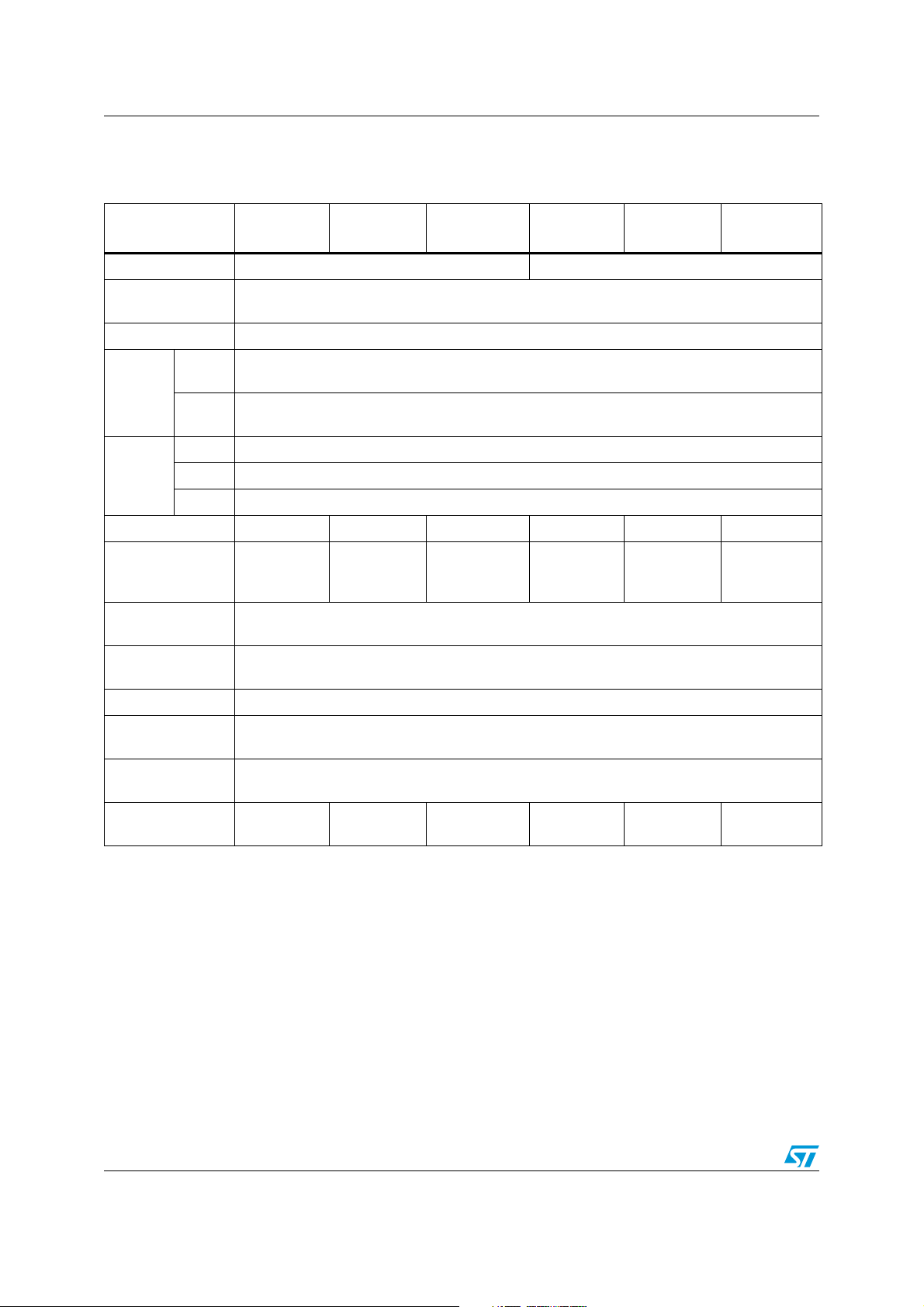
Table 1. Low density STM8L15xxx low power device features and peripheral counts
Features STM8L151F3 STM8L151G3
STM8L151K3/
STM8L151C3
STM8L151F2 STM8L151G2
STM8L151K2/
STM8L151C2
Flash (Kbytes) 8 4
Data EEPROM
(bytes)
256
RAM (Kbytes) 1
Basic
1
(8-bit)
Timers
General
purpose
Commun
-ication
interfaces
SPI 1
I2C 1
USART 1
GPIOs 18
12-bit synchronized
ADC (number of
channels)
(10)
Comparators
(COMP1/COMP2)
Others
(1)
1
26
(18)
(1)
1
30
(2)
/41
1
(23/28)
RTC, window watchdog, independent watchdog,
16-MHz and 38-kHz internal RC, 1- to 16-MHz and 32-kHz external oscillator
2
(16-bit)
(1)(2)
18
(3)
2
1
(10)
(1)
26
(18)
(1)
1
CPU frequency 16 MHz
Operating voltage
Operating
temperature
1.8 to 3.6 V (down to 1.65 V at power-down) with BOR
1.65 to 3.6 V without BOR
− 40 to +85 °C / − 40 to +125 °C
(2)
30
(23/28)
/41
1
(1)(2)
(3)
Packages
1. The number of GPIOs given in this table includes the NRST/PA1 pin but the application can use the NRST/PA1 pin as
general purpose output only (PA1).
2. 26 GPIOs in the STM8L151K3 and 40 GPIOs in the STM8L151C3.
3. 22 channels in the STM8L151K3 and 28 channels in the STM8L151C3.
TSSOP20
UFQFPN20
UFQFPN28
UFQFPN32
LQFP48
TSSOP20
UFQFPN20
UFQFPN28
UFQFPN32
LQFP48
12/112 Doc ID 018780 Rev 4

STM8L151x2, STM8L151x3 Description
2.2 Ultra-low-power continuum
The ultra-low-power Low density STM8L15xxx devices are fully pin-to-pin, software and
feature compatible. Besides the full compatibility within the family, the devices are part of
STMicroelectronics microcontrollers ultra-low-power strategy which also includes
STM8L101xx and STM32L15xxx. The STM8L and STM32L families allow a continuum of
performance, peripherals, system architecture, and features.
They are all based on STMicroelectronics 0.13 µm ultra-low leakage process.
Note: 1 The STM8L151xx and STM8L152xx are pin-to-pin compatible with STM8L101xx devices.
Performance
All families incorporate highly energy-efficient cores with both Harvard architecture and
pipelined execution: advanced STM8 core for STM8L families and ARM Cortex™-M3 core
for STM32L family. In addition specific care for the design architecture has been taken to
optimize the mA/DMIPS and mA/MHz ratios.
This allows the ultra-low-power performance to range from 5 up to 33.3 DMIPs.
Shared peripherals
STM8L151xx/152xx and STM32L15xx share identical peripherals which ensure a very easy
migration from one family to another:
● Analog peripherals: ADC1 and comparators COMP1/COMP2
● Digital peripherals: RTC and some communication interfaces
Common system strategy
To offer flexibility and optimize performance, the STM8L151xx/152xx and STM32L15xx
devices use a common architecture:
● Same power supply range from 1.8 to 3.6 V, down to 1.65 V at power down
● Architecture optimized to reach ultra-low consumption both in low power modes and
Run mode
● Fast startup strategy from low power modes
● Flexible system clock
● Ultra-safe reset: same reset strategy for both STM8L15x and STM32L15xxx including
power-on reset, power-down reset, brownout reset and programmable voltage detector.
Features
ST ultra-low-power continuum also lies in feature compatibility:
● More than 10 packages with pin count from 20 to 100 pins and size down to 3 x 3 mm
● Memory density ranging from 4 to 128 Kbytes
Doc ID 018780 Rev 4 13/112
Functional overview STM8L151x2, STM8L151x3
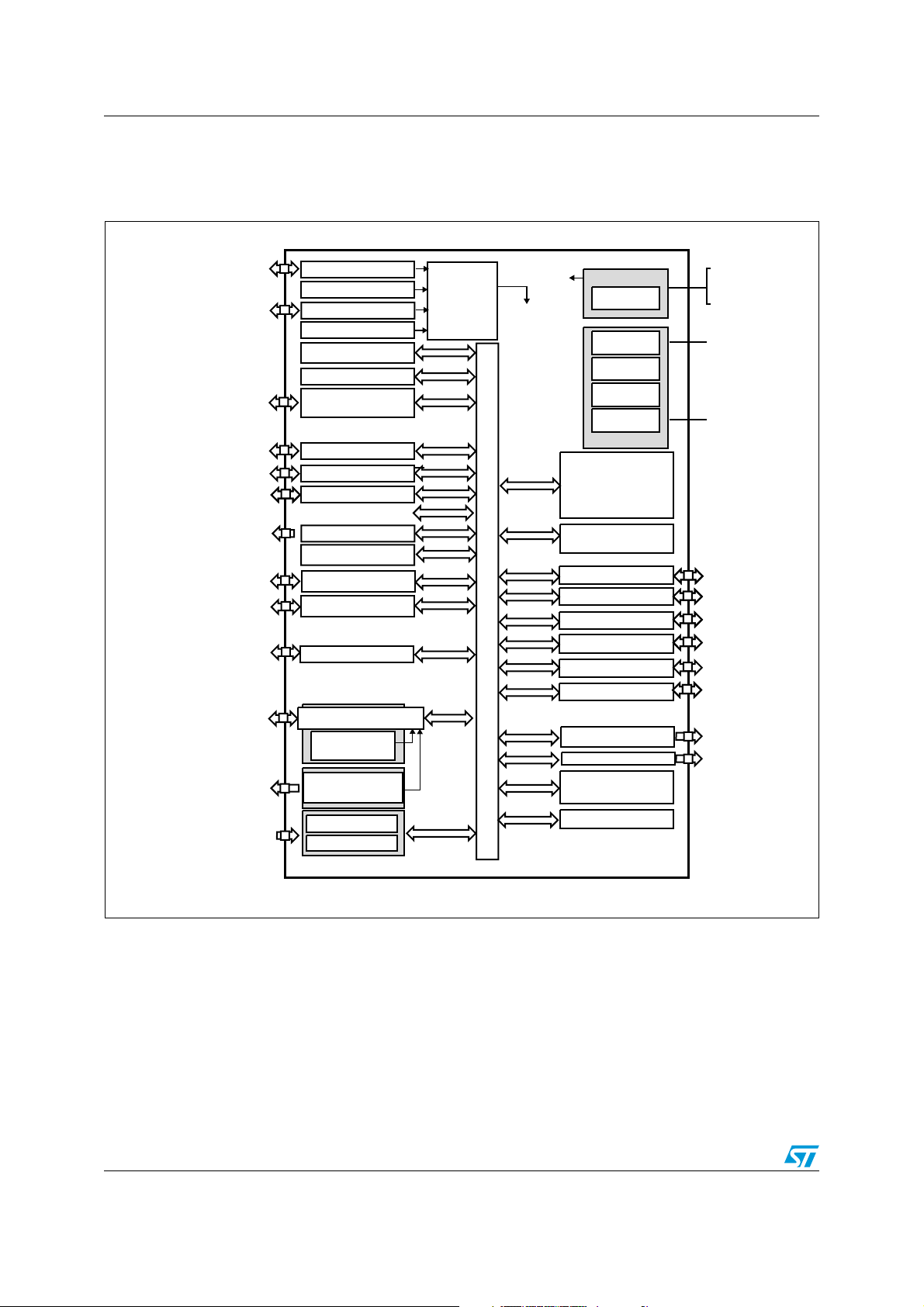
MS18275V2
Clock
controller
and CSS
Clocks
Address, control and data buses
8-Kbyte
1-Kbyte RAM
to core and
peripherals
IWDG
(38 kHz clock)
Port A
Port B
Port C
Power
VOLT. REG.
WWDG
256-byte
Port D
Port E
Beeper
RTC
memoryProgram
Data EEPROM
@V
DD
V
DD18
V
DD
=1.65 V
V
SS
SWIM
SCL, SDA,
SPI1_MOSI, SPI1_MISO,
SPI1_SCK, SPI1_NSS
USART1_RX, USART1_TX,
USART1_CK
ADC1_INx
COMP1_INP
COMP 1
COMP 2
COMP2_INP
V
DDA, VSSA
SMB
@V
DDA/VSSA
Temp sensor
12-bit ADC1
V
DDREF
3.6 V
NRST
PA[7:0]
PB[7:0]
PC[7:0]
PD[7:0]
PE[7:0]
PF0
BEEP
ALARM, CALIB,
POR/PDR
OSC_IN,
OSC_OUT
OSC32_IN,
OSC32_OUT
to
BOR
PVD
PVD_IN
RESET
DMA1 (4 channels)
2 channels
2 channels
COMP2_INM
Internal reference
voltage
VREFINT out
IR_TIM
1-16 MHz oscillator
16 MHz internal RC
32 kHz oscillator
STM8 Core
16-bit Timer 2
38 kHz internal RC
Interrupt controller
16-bit Timer 3
Debug module
(SWIM)
8-bit Timer 4
Infrared interface
SPI1
I²C1
USART1
V
SSREF
Port F
up to
(2)
(2)
(2)
3 Functional overview
Figure 1. Low density STM8L151xx device block diagram
1. Legend:
ADC: Analog-to-digital converter
BOR: Brownout reset
DMA: Direct memory access
I²C: Inter-integrated circuit multimaster interface
IWDG: Independent watchdog
POR/PDR: Power on reset / power down reset
RTC: Real-time clock
SPI: Serial peripheral interface
SWIM: Single wire interface module
USART: Universal synchronous asynchronous receiver transmitter
WWDG: Window watchdog
2. There is no TIM1 on STM8L151x2, STM8L151x3 devices.
14/112 Doc ID 018780 Rev 4

STM8L151x2, STM8L151x3 Functional overview
3.1 Low power modes
The Low density STM8L15x devices support five low power modes to achieve the best
compromise between low power consumption, short startup time and available wakeup
sources:
● Wait mode: The CPU clock is stopped, but selected peripherals keep running. An
internal or external interrupt or a Reset can be used to exit the microcontroller from
Wait mode (WFE or WFI mode). Wait consumption: refer to Tabl e 1 7.
● Low power run mode: The CPU and the selected peripherals are running. Execution
is done from RAM with a low speed oscillator (LSI or LSE). Flash and data EEPROM
are stopped and the voltage regulator is configured in ultra-low-power mode. The
microcontroller enters Low power run mode by software and can exit from this mode by
software or by a reset.
All interrupts must be masked. They cannot be used to exit the microcontroller from this
mode. Low power run mode consumption: refer to Ta bl e 1 8 .
● Low power wait mode: This mode is entered when executing a Wait for event in Low
power run mode. It is similar to Low power run mode except that the CPU clock is
stopped. The wakeup from this mode is triggered by a Reset or by an internal or
external event (peripheral event generated by the timers, serial interfaces, DMA
controller (DMA1), comparators and I/O ports). When the wakeup is triggered by an
event, the system goes back to Low power run mode.
All interrupts must be masked. They cannot be used to exit the microcontroller from this
mode. Low power wait mode consumption: refer to Tab le 1 9.
● Active-halt mode: CPU and peripheral clocks are stopped, except RTC. The wakeup
can be triggered by RTC interrupts, external interrupts or reset. Active-halt
consumption: refer to Tab l e 2 0 and Ta bl e 2 1 .
● Halt mode: CPU and peripheral clocks are stopped, the device remains powered on.
The RAM content is preserved. The wakeup is triggered by an external interrupt or
reset. A few peripherals have also a wakeup from Halt capability. Switching off the
internal reference voltage reduces power consumption. Through software configuration
it is also possible to wake up the device without waiting for the internal reference
voltage wakeup time to have a fast wakeup time of 5 µs. Halt consumption: refer to
Ta bl e 2 2 .
3.2 Central processing unit STM8
3.2.1 Advanced STM8 Core
The 8-bit STM8 core is designed for code efficiency and performance with an Harvard
architecture and a 3-stage pipeline.
It contains 6 internal registers which are directly addressable in each execution context, 20
addressing modes including indexed indirect and relative addressing, and 80 instructions.
Doc ID 018780 Rev 4 15/112

Functional overview STM8L151x2, STM8L151x3
Architecture and registers
● Harvard architecture
● 3-stage pipeline
● 32-bit wide program memory bus - single cycle fetching most instructions
● X and Y 16-bit index registers - enabling indexed addressing modes with or without
offset and read-modify-write type data manipulations
● 8-bit accumulator
● 24-bit program counter - 16 Mbyte linear memory space
● 16-bit stack pointer - access to a 64 Kbyte level stack
● 8-bit condition code register - 7 condition flags for the result of the last instruction
Addressing
● 20 addressing modes
● Indexed indirect addressing mode for lookup tables located anywhere in the address
space
● Stack pointer relative addressing mode for local variables and parameter passing
Instruction set
● 80 instructions with 2-byte average instruction size
● Standard data movement and logic/arithmetic functions
● 8-bit by 8-bit multiplication
● 16-bit by 8-bit and 16-bit by 16-bit division
● Bit manipulation
● Data transfer between stack and accumulator (push/pop) with direct stack access
● Data transfer using the X and Y registers or direct memory-to-memory transfers
3.2.2 Interrupt controller
The Low density STM8L15x features a nested vectored interrupt controller:
● Nested interrupts with 3 software priority levels
● 32 interrupt vectors with hardware priority
● Up to 40 external interrupt sources on 11 vectors
● Trap and reset interrupts
16/112 Doc ID 018780 Rev 4

STM8L151x2, STM8L151x3 Functional overview
3.3 Reset and supply management
3.3.1 Power supply scheme
The device requires a 1.65 V to 3.6 V operating supply voltage (VDD). The external power
supply pins must be connected as follows:
● V
● V
● V
● V
3.3.2 Power supply supervisor
The device has an integrated ZEROPOWER power-on reset (POR)/power-down reset
(PDR), coupled with a brownout reset (BOR) circuitry. At power-on, BOR is always active,
and ensures proper operation starting from 1.8 V. After the 1.8 V BOR threshold is reached,
the option byte loading process starts, either to confirm or modify default thresholds, or to
disable BOR permanently (in which case, the V
Five BOR thresholds are available through option bytes, starting from 1.8 V to 3 V. To
reduce the power consumption in Halt mode, it is possible to automatically switch off the
internal reference voltage (and consequently the BOR) in Halt mode. The device remains
under reset when V
for any external reset circuit.
SS1
; V
= 1.8 to 3.6 V, down to 1.65 V at power down: external power supply for
DD1
I/Os and for the internal regulator. Provided externally through V
corresponding ground pin is V
SSA ; VDDA
= 1.8 to 3.6 V, down to 1.65 V at power down: external power supplies for
analog peripherals (minimum voltage to be applied to V
used). V
SS2
I/Os. V
REF+
externally through V
and V
DDA
; V
= 1.8 to 3.6 V, down to 1.65 V at power down: external power supplies for
DD2
and V
DD2
; V
(for ADC1): external reference voltage for ADC1. Must be provided
REF-
DD
must be connected to V
SSA
must be connected to V
SS2
and V
REF+
is below a specified threshold, V
SS1
REF-
.
pin.
is 1.8 V when the ADC1 is
DDA
and V
DD1
and V
DD1
min value at power down is 1.65 V).
DD
POR/PDR
, respectively.
SS1
, respectively.
SS1
or V
pins, the
DD1
, without the need
BOR
The device features an embedded programmable voltage detector (PVD) that monitors the
V
DD/VDDA
power supply and compares it to the V
levels between 1.85 V and 3.05 V, chosen by software, with a step around 200 mV. An
interrupt can be generated when V
V
DD/VDDA
is higher than the V
a warning message and/or put the MCU into a safe state. The PVD is enabled by software.
3.3.3 Voltage regulator
The Low density STM8L15x embeds an internal voltage regulator for generating the 1.8 V
power supply for the core and peripherals.
This regulator has two different modes:
● Main voltage regulator mode (MVR) for Run, Wait for interrupt (WFI) and Wait for event
(WFE) modes.
● Low power voltage regulator mode (LPVR) for Halt, Active-halt, Low power run and Low
power wait modes.
When entering Halt or Active-halt modes, the system automatically switches from the MVR
to the LPVR in order to reduce current consumption.
threshold. This PVD offers 7 different
PVD
DD/VDDA
threshold. The interrupt service routine can then generate
PVD
Doc ID 018780 Rev 4 17/112
drops below the V
threshold and/or when
PVD

Functional overview STM8L151x2, STM8L151x3
3.4 Clock management
The clock controller distributes the system clock (SYSCLK) coming from different oscillators
to the core and the peripherals. It also manages clock gating for low power modes and
ensures clock robustness.
Features
● Clock prescaler: to get the best compromise between speed and current consumption
the clock frequency to the CPU and peripherals can be adjusted by a programmable
prescaler
● Safe clock switching: Clock sources can be changed safely on the fly in run mode
through a configuration register.
● Clock management: To reduce power consumption, the clock controller can stop the
clock to the core, individual peripherals or memory.
● System clock sources: 4 different clock sources can be used to drive the system
clock:
– 1-16 MHz High speed external crystal (HSE)
– 16 MHz High speed internal RC oscillator (HSI)
– 32.768 kHz Low speed external crystal (LSE)
– 38 kHz Low speed internal RC (LSI)
● RTC clock sources: the above four sources can be chosen to clock the RTC whatever
the system clock.
● Startup clock: After reset, the microcontroller restarts by default with an internal
2 MHz clock (HSI/8). The prescaler ratio and clock source can be changed by the
application program as soon as the code execution starts.
● Clock security system (CSS): This feature can be enabled by software. If a HSE clock
failure occurs, the system clock is automatically switched to HSI.
● Configurable main clock output (CCO): This outputs an external clock for use by the
application.
18/112 Doc ID 018780 Rev 4

STM8L151x2, STM8L151x3 Functional overview
Figure 2. Low density STM8L15x clock tree diagram
SWIM[3:0]
OSC_OUT
OSC_IN
OSC32_OUT
OSC32_IN
CCO
HSE OSC
1-16 MHz
HSI RC
1-16 MHz
LSI RC
38 kHz
LSE OSC
32.768 kHz
Configurable
clock output
CCO
prescaler
/1;2;4;8;16;32;64
HSE
HSI
LSI
LSE
LSE
CLKBEEPSEL[1:0]
LSI
RTCSEL[3:0]
/1;2;4;8;16;32;64
CCOSEL[3:0]
SYSCLK
prescaler
/1;2;4;8;16;32;64
RTC
prescaler
HSI
LSI
HSE
LSE
SYSCLK to core and
Peripheral
Clock
enable (13 bits)
BEEPCLK
IWDGCLK
RTCCLK
memory
PCLK to
peripherals
to
BEEP
to
IWDG
to
RTC
MS18281V1
3.5 Low power real-time clock
The real-time clock (RTC) is an independent binary coded decimal (BCD) timer/counter.
Six byte locations contain the second, minute, hour (12/24 hour), week day, date, month,
year, in BCD (binary coded decimal) format. Correction for 28, 29 (leap year), 30, and 31
day months are made automatically.
It provides a programmable alarm and programmable periodic interrupts with wakeup from
Halt capability.
● Periodic wakeup time using the 32.768 kHz LSE with the lowest resolution (of 61 µs) is
from min. 122 µs to max. 3.9 s. With a different resolution, the wakeup time can reach
36 hours
● Periodic alarms based on the calendar can also be generated from every second to
every year
Doc ID 018780 Rev 4 19/112

Functional overview STM8L151x2, STM8L151x3
3.6 Memories
The Low density STM8L15x devices have the following main features:
● Up to 1 Kbyte of RAM
● The non-volatile memory is divided into three arrays:
– Up to 8 Kbytes of low-density embedded Flash program memory
– 256 bytes of data EEPROM
–Option bytes.
The EEPROM embeds the error correction code (ECC) feature.
The option byte protects part of the Flash program memory from write and readout piracy.
3.7 DMA
A 4-channel direct memory access controller (DMA1) offers a memory-to-memory and
peripherals-from/to-memory transfer capability. The 4 channels are shared between the
following IPs with DMA capability: ADC1, I2C1, SPI1, USART1, the three Timers.
3.8 Analog-to-digital converter
● 12-bit analog-to-digital converter (ADC1) with 25 channels (including 1 fast channel),
temperature sensor and internal reference voltage
● Conversion time down to 1 µs with f
● Programmable resolution
● Programmable sampling time
● Single and continuous mode of conversion
● Scan capability: automatic conversion performed on a selected group of analog inputs
● Analog watchdog
● Triggered by timer
SYSCLK
Note: ADC1 can be served by DMA1.
3.9 Ultra-low-power comparators
The Low density STM8L15x embeds two comparators (COMP1 and COMP2) sharing the
same current bias and voltage reference. The voltage reference can be internal or external
(coming from an I/O).
● One comparator with fixed threshold (COMP1).
● One comparator rail to rail with fast or slow mode (COMP2). The threshold can be one
of the following:
– External I/O
– Internal reference voltage or internal reference voltage submultiple (1/4, 1/2, 3/4)
= 16 MHz
The two comparators can be used together to offer a window function. They can wake up
from Halt mode.
20/112 Doc ID 018780 Rev 4

STM8L151x2, STM8L151x3 Functional overview
3.10 System configuration controller and routing interface
The system configuration controller provides the capability to remap some alternate
functions on different I/O ports. TIM4 and ADC1 DMA channels can also be remapped.
The highly flexible routing interface controls the routing of internal analog signals to ADC1,
COMP1, COMP2, and the internal reference voltage V
. It also provides a set of
REFINT
registers for efficiently managing the charge transfer acquisition sequence (Section 3.11:
Touchsensing).
3.11 Touchsensing
Low density STM8L15xxx devices provide a simple solution for adding capacitive sensing
functionality to any application. Capacitive sensing technology is able to detect finger
presence near an electrode which is protected from direct touch by a dielectric (example,
glass, plastic). The capacitive variation introduced by a finger (or any conductive object) is
measured using a proven implementation based on a surface charge transfer acquisition
principle. It consists of charging the electrode capacitance and then transferring a part of the
accumulated charges into a sampling capacitor until the voltage across this capacitor has
reached a specific threshold. In Low density STM8L15xxx devices, the acquisition sequence
is managed either by software or by hardware and it involves analog I/O groups, the routing
interface, and timers.Reliable touch sensing solutions can be quickly and easily
implemented using the free STM8 Touch Sensing Library.
3.12 Timers
Low density STM8L15x devices contain two 16-bit general purpose timers (TIM2 and TIM3)
and one 8-bit basic timer (TIM4).
All the timers can be served by DMA1.
Ta bl e 2 compares the features of the advanced control, general-purpose and basic timers.
Table 2. Timer feature comparison
Timer
TIM2
TIM3
TIM4 8-bit up
Counter
resolution
16-bit up/down
Counter
type
Prescaler factor
Any power of 2
from 1 to 128
Any power of 2
from 1 to 32768
DMA1
request
generation
Ye s
Capture/compare
channels
2
0
Complementary
outputs
None
Doc ID 018780 Rev 4 21/112

Functional overview STM8L151x2, STM8L151x3
3.12.1 16-bit general purpose timers
● 16-bit autoreload (AR) up/down-counter
● 7-bit prescaler adjustable to fixed power of 2 ratios (1…128)
● 2 individually configurable capture/compare channels
● PWM mode
● Interrupt capability on various events (capture, compare, overflow, break, trigger)
● Synchronization with other timers or external signals (external clock, reset, trigger and
enable)
3.12.2 8-bit basic timer
The 8-bit timer consists of an 8-bit up auto-reload counter driven by a programmable
prescaler. It can be used for timebase generation with interrupt generation on timer overflow.
3.13 Watchdog timers
The watchdog system is based on two independent timers providing maximum security to
the applications.
3.13.1 Window watchdog timer
The window watchdog (WWDG) is used to detect the occurrence of a software fault, usually
generated by external interferences or by unexpected logical conditions, which cause the
application program to abandon its normal sequence.
3.13.2 Independent watchdog timer
The independent watchdog peripheral (IWDG) can be used to resolve processor
malfunctions due to hardware or software failures.
It is clocked by the internal LSI RC clock source, and thus stays active even in case of a
CPU clock failure.
3.14 Beeper
The beeper function outputs a signal on the BEEP pin for sound generation. The signal is in
the range of 1, 2 or 4 kHz.
22/112 Doc ID 018780 Rev 4

STM8L151x2, STM8L151x3 Functional overview
3.15 Communication interfaces
3.15.1 SPI
The serial peripheral interface (SPI1) provides half/ full duplex synchronous serial
communication with external devices.
● Maximum speed: 8 Mbit/s (f
● Full duplex synchronous transfers
● Simplex synchronous transfers on 2 lines with a possible bidirectional data line
● Master or slave operation - selectable by hardware or software
● Hardware CRC calculation
● Slave/master selection input pin
SYSCLK
Note: SPI1 can be served by the DMA1 Controller.
3.15.2 I²C
The I2C bus interface (I2C1) provides multi-master capability, and controls all I²C busspecific sequencing, protocol, arbitration and timing.
● Master, slave and multi-master capability
● Standard mode up to 100 kHz and fast speed modes up to 400 kHz.
● 7-bit and 10-bit addressing modes.
● SMBus 2.0 and PMBus support
● Hardware CRC calculation
Note: I
2
C1 can be served by the DMA1 Controller.
/2) both for master and slave
3.15.3 USART
The USART interface (USART1) allows full duplex, asynchronous communications with
external devices requiring an industry standard NRZ asynchronous serial data format. It
offers a very wide range of baud rates.
● 1 Mbit/s full duplex SCI
● SPI1 emulation
● High precision baud rate generator
● Smartcard emulation
● IrDA SIR encoder decoder
● Single wire half duplex mode
Note: USART1 can be served by the DMA1 Controller.
3.16 Infrared (IR) interface
The Low density STM8L15x devices contain an infrared interface which can be used with an
IR LED for remote control functions. Two timer output compare channels are used to
generate the infrared remote control signals.
Doc ID 018780 Rev 4 23/112

Functional overview STM8L151x2, STM8L151x3
3.17 Development support
Development tools
Development tools for the STM8 microcontrollers include:
● The STice emulation system offering tracing and code profiling
● The STVD high-level language debugger including C compiler, assembler and
integrated development environment
● The STVP Flash programming software
The STM8 also comes with starter kits, evaluation boards and low-cost in-circuit
debugging/programming tools.
Single wire data interface (SWIM) and debug module
The debug module with its single wire data interface (SWIM) permits non-intrusive real-time
in-circuit debugging and fast memory programming.
The Single wire interface is used for direct access to the debugging module and memory
programming. The interface can be activated in all device operation modes.
The non-intrusive debugging module features a performance close to a full-featured
emulator. Beside memory and peripherals, CPU operation can also be monitored in realtime by means of shadow registers.
Bootloader
The Low density STM8L15xxx Ultralow power devices feature a built-in bootloader (see
UM0560: STM8 bootloader user manual).
The bootloader is used to download application software into the device memories,
including RAM, program and data memory, using standard serial interfaces. It is a
complementary solution to programming via the SWIM debugging interface.
24/112 Doc ID 018780 Rev 4

STM8L151x2, STM8L151x3 Pin description
12
17
1
2
3
4
5
6
7
8
9
10
11
NRST/PA1
PA2
PA3
PA4
PE0
PE1
PD1
PD2
PD3
PE3
PD0
PE5
PE4
V
DD
V
DDA
V
REF+
PE2
PB2
PC0
PC1
PC2
PC3
PC4
PC5
PC6
PC7
PE6
PE7
PB3
PB4
PB5
PB6
PB7
PF0
PD4
PD5
PD6
PD7
PA0
PA5
13 14
15
16
PA6
PA7
/V
SSA/VREF-
V
SS1
PB0
V
SSIO
V
DDIO
3738394142434445464748 40
24 23 22 21 20 19 18
35
34
33
32
31
30
29
28
27
26
25
PB1
36
Res.
(1)
MS18276V1
1
2
3
4
5
6
7
8
13 14 15 16
17
18
19
20
21
22
23
24
32
28 27 26 25
PA5
V
SS1
NRST/PA1
PA2
PA3
PA4
PA6
V
DD1
PD3
PB0
PB1
PD0
PD1
PD2
PB3
PB2
PB5
PB4
PD4
PB7
PB6
PD7
PD6
PD5
PC0
PC3
PC2
PC1
PC4
PC5
PC6
PA0
MS18277V1
31 30 29
1291011
PD3
PB0
PB1
PB2
PD0
PD1
PD2
PA 5
V
SS1/VSSA/VREF-
V
DD1/VDDA/VREF+
NRST/PA1
PA 2
PA 4
PB6
PB5
PB4
PB3
PC0
PD4
PB7
PC4
PC3
PC2
PC1
PA 0
PC6
PC5
2
1
3
4
5
6
7
981011121314
20
21
19
18
17
16
15
2728 26 25 24 23 22
PA 3
ai18250
4 Pin description
Figure 3. STM8L151Cx LQFP48 package pinout
Figure 4. STM8L151Kx UFQFPN32 package pinout
Figure 5. STM8L151Gx UFQFPN28 package pinout
Doc ID 018780 Rev 4 25/112

Pin description STM8L151x2, STM8L151x3
2
1
3
4
5
67 8
9
11
12
13
14
15
91817161
PD0
V
DD/VDDA/VREF+
VSS/V
SSA/VREF-
PA3
PA2
PB0
NRST / PA1
PC5
PC6
PC4
PC1
PB4
PB5
PB6
PB7
PC0
PB1
PB2
10
PB3
PA0
20
MS18279V1
PA 3
PA2
VSS/V
SSA/VREF-
NRST / PA1
PC0
PC1
PB7
PB6
PB1
PB2
PB3
PB4
PB5
VDD/V
DDA/VREF+
PC4
1
2
3
4
5
6
7
10
9
8
20
19
18
17
16
15
14
11
12
13
MS18280V1
PB 0
PD0
PA0
PC6
PC5
Figure 6. STM8L151Fx UFQFPN20 package pinout
Figure 7. STM8L151Fx TSSOP20 package pinout
26/112 Doc ID 018780 Rev 4

STM8L151x2, STM8L151x3 Pin description
Table 3. Legend/abbreviation for table 4
Typ e I= input, O = output, S = power supply
Level
Output HS = high sink/source (20 mA)
FT Five-volt tolerant
Port and control
configuration
Input float = floating, wpu = weak pull-up
Output T = true open drain, OD = open drain, PP = push pull
Bold X (pin state after reset release).
Reset state
Unless otherwise specified, the pin state is the same during the reset phase (i.e.
“under reset”) and after internal reset release (i.e. at reset state).
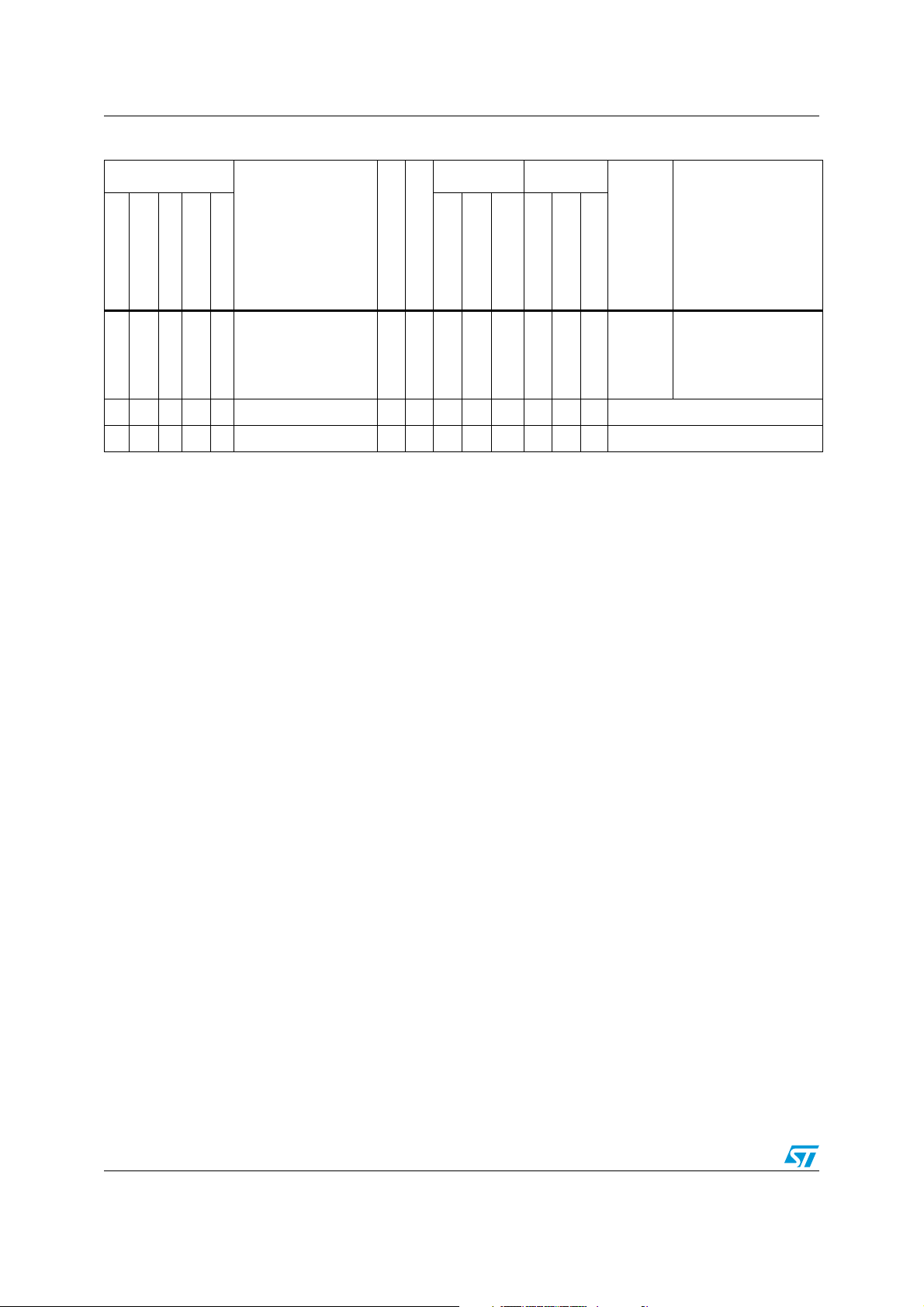
Table 4. Low density STM8L15xxx pin description
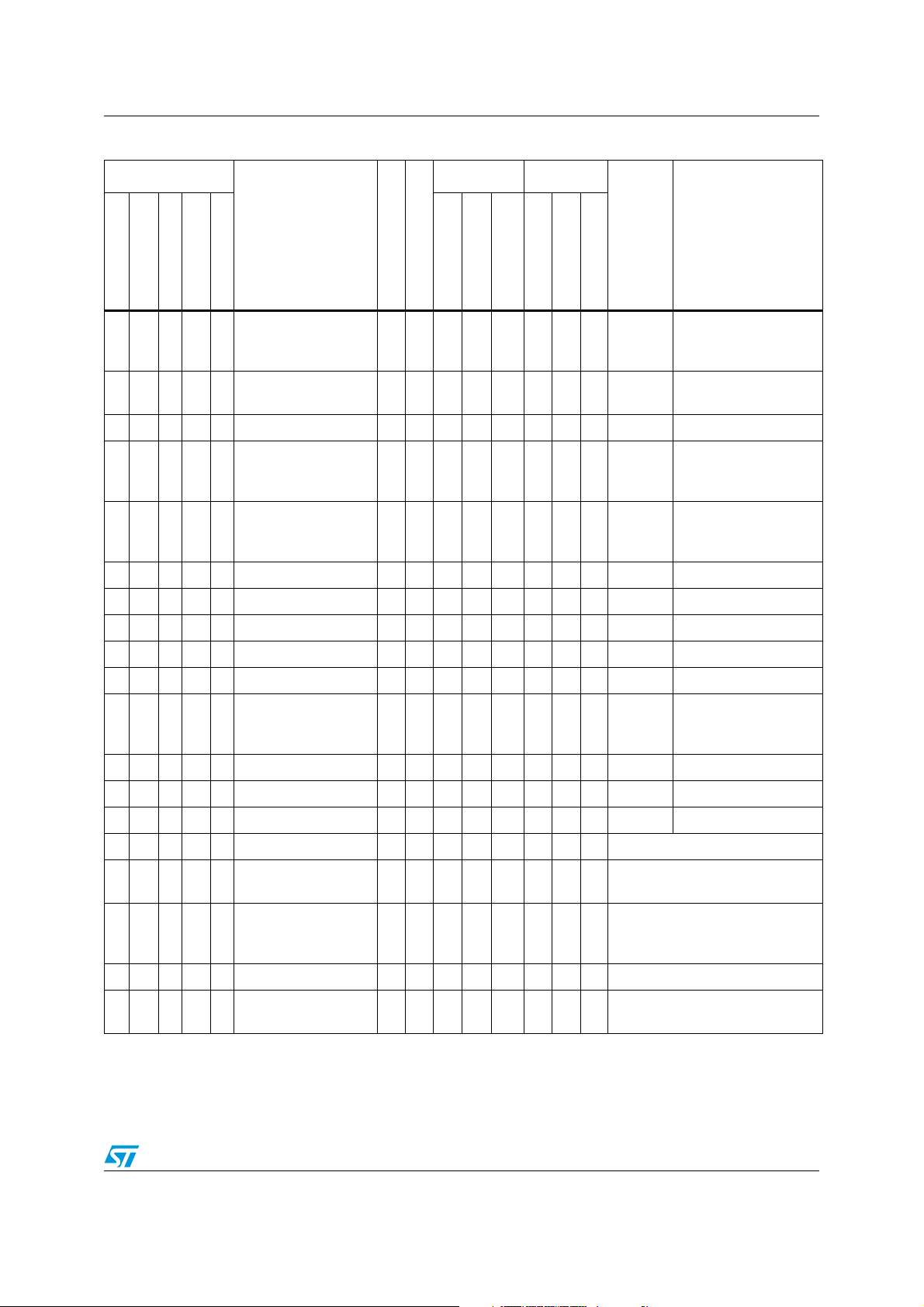
Pin number
LQFP48
21114NRST/PA1
32225
43336
544- -
Input Output
Pin name
UFQFPN32
UFQFPN28
TSSOP20
UFQFPN20
PA2/OSC_IN/
[USART_TX]
[SPI_MISO]
PA3/OSC_OUT/[USA
RT_RX]
]
(2)
(2)
PA4/TIM2_BKIN/
[TIM2_ETR]
(1)
(2)
/
(2)
/[SPI_MOSI
(2)
Typ e
I/O level
floating
I/O X HS X Reset PA 1
I/O X XXHSXXPort A2
I/O X XXHSXXPort A3
I/O X XXHSXXPort A4
ADC1_IN2
655- -
PA5/TIM3_BKIN/
[TIM3_ETR]
(2)
/ADC1_
I/O X XXHSXXPort A5
IN1
wpu
Ext. interrupt
Default alternate
function
PP
OD
(after reset)
Main function
High sink/source
HSE oscillator input /
[USART transmit] / [SPI
master in- slave out] /
HSE oscillator output /
[USART receive]/ [SPI
master out/slave in]/
Timer 2 - break input /
[Timer 2 - external
trigger] /ADC1 input 2
Timer 3 - break input /
[Timer 3 - external
trigger] /
ADC1input 1
76- - -
PA6/ADC1_TRIG/
ADC1_IN0
I/O X XXHSXXPort A6
8----PA7 I/O X XXHSXXPort A7
24 13 12 7 10
25 14 13 8 11
26 15 14 9 12
PB0
ADC1_IN18
PB1/TIM3_CH1/
ADC1_IN17
PB2/ TIM2_CH2/
ADC1_IN16
I/O X XXHSXXPort B0
I/O X XXHSXXPort B1
I/O X XXHSXXPort B2
(3)
/TIM2_CH1/
PB3/TIM2_ETR/
27 16 15 10 13
ADC1_IN15/RTC_AL
(4)
ARM
I/O X XXHSXXPort B3
Doc ID 018780 Rev 4 27/112
ADC1- trigger
/ADC1input 0
Timer 2 - channel 1 /
ADC1_IN18
Timer 3 - channel 1 /
ADC1_IN17
Timer 2 - channel 2
ADC1_IN16
Timer 2 - external
trigger / ADC1_IN15 /
RTC_ALARM
(4)

Pin description STM8L151x2, STM8L151x3
Table 4. Low density STM8L15xxx pin description (continued)
Pin number
LQFP48
UFQFPN32
UFQFPN28
UFQFPN20
Pin name
TSSOP20
Type
Input Output
I/O level
wpu
floating
OD
Ext. interrupt
High sink/source
(3)
/SPI1_NSS/
28 17 16 11 14
29 18 17 12 15
30 19 18 13 16
31 20 19 14 17
PB4
ADC1_IN14
PB5/SPI_SCK/
/ADC1_IN13
PB6/SPI1_MOSI/
ADC1_IN12
PB7/SPI1_MISO/
ADC1_IN11
37 25 21 15 18 PC0/I2C_SDA I/O FT X XT
38 26 22 16 19 PC1/I2C_SCL I/O FT X XT
41 27 23 - -
42 28 24 - -
PC2/USART_RX/ADC
1_IN6
PC3/USART_TX/
ADC1_IN5
I/O X XXHSXXPort B4
I/O X XXHSXXPort B5
I/O X XXHSXXPort B6
I/O X XXHSXXPort B7
(5)
(3)
I/O X XXHSXXPort C2
I/O X XXHSXXPort C3
PC4/USART_CK]/
43 29 25 17 20
I2C_SMB/CCO/
I/O X XXHSXXPort C4
ADC1_IN4
Default alternate
PP
(after reset)
Main function
SPI master/slave select
/ ADC1_IN14
[SPI clock] /
ADC1_IN13
SPI master out/
slave in / ADC1_IN12
SPI1 master in- slave
out/
ADC1_IN11
Port C0 I2C data
Port C1 I2C clock
USART receive /
ADC1_IN6
USART transmit /
ADC1_IN5
USART synchronous
clock / I2C1_SMB /
Configurable clock
output / ADC1_IN4
function
LSE oscillator input /
[SPI master/slave
select] / [USART
transmit]/
Timer 2 -channel 1
LSE oscillator output /
[SPI clock] / [USART
receive]/
Timer 2 -channel 2
44 30 26 18 1
45 31 27 19 2
PC5/OSC32_IN
/[SPI1_NSS]
[USART_TX]
TIM2_CH1
PC6/OSC32_OUT/
[SPI_SCK]
[USART_RX]
TIM2_CH2
(6)
(2)
(6)
(2)
(2)
/
(2)
/
/
/
I/O X XXHSXXPort C5
I/O X XXHSXXPort C6
46----PC7/ADC1_IN3 I/O X XXHSXXPort C7 ADC1_IN3
Timer 3 - channel 2 /
[ADC1_Trigger] /
ADC1_IN22
Timer 3 - external
trigger / ADC1_IN21
209869
21 10 9 - -
22 11 10 - -
PD0/TIM3_CH2/
[ADC1_TRIG]
(2)
ADC1_IN22
PD1/TIM3_ETR/
ADC1_IN21
PD2/
ADC1_IN20
/
I/O X XXHSXXPort D0
I/O X XXHSXXPort D1
I/O X XXHSXXPort D2 ADC1_IN20
28/112 Doc ID 018780 Rev 4
(6)
(6)
STM8L151x2, STM8L151x3 Pin description
Table 4. Low density STM8L15xxx pin description (continued)
Pin number
LQFP48
UFQFPN32
UFQFPN28
UFQFPN20
Pin name
TSSOP20
Type
Input Output
I/O level
wpu
floating
OD
Ext. interrupt
PP
Main function
Default alternate
function
(after reset)
High sink/source
23 12 11 - -
33 21 20 - -
PD3/
ADC1_IN19/
RTC_CALIB
PD4/
ADC1_IN10
(7)
I/O X XXHSXXPort D3
I/O X XXHSXXPort D4 ADC1_IN10
ADC1_IN19/
RTC calibration
34 22 - - - PD5/ ADC1_IN9 I/O X XXHSXXPort D5 ADC1_IN9
-23- - -
PD6/
ADC1_IN8/RTC_CALIBI/O X XXHSXXPort D6
ADC1_IN8 / RTC
calibration
PD7
36 24 - - -
/ADC1_IN7/RTC_ALARMI/O X XXHSXXPort D7 ADC1_IN7 / RTC alarm
14----PE0 I/O X XXHSXXPort E0
15----PE1 I/O X XXHSXXPort E1
16----PE2 I/O X XXHSXXPort E2
17 - - - - PE3/ADC1_IN26 I/O X XXHSXXPort E3 ADC1_IN26
(7)
18 - - - - PE4/ADC1_IN27 I/O X XXHSXXPort E4 ADC1_IN27
ADC1_IN23/
Comparator positive
input
19----
PE5/ADC1_IN23/
COMP_INP
I/O X XXHSXXPort E5
47 - - - - PE6/PVD_IN I/O X XXHSXXPort E6 PVD_IN
48 - - - - PE7/ADC1_IN25 I/O X XXHSXXPort E7 ADC1_IN25
32----PF0/ADC1_IN24 I/O X XXHSXXPort F0 ADC1_IN24
10----V
- 8758V
DD
DD /VDDA
/ V
REF+
S Digital supply voltage
S
Digital supply voltage /
ADC1 positive voltage reference
Ground voltage / ADC1 negative
97647V
SS
REF-
/ V
SSA
voltage reference / Analog ground
/ V
voltage
11----V
12----V
DDA
REF+
S Analog supply voltage
S
ADC1 positive voltage
reference
Doc ID 018780 Rev 4 29/112
Pin description STM8L151x2, STM8L151x3
Table 4. Low density STM8L15xxx pin description (continued)
Pin number
LQFP48
UFQFPN32
UFQFPN28
UFQFPN20
Pin name
TSSOP20
Type
Input Output
I/O level
wpu
floating
OD
Ext. interrupt
PP
Main function
Default alternate
function
(after reset)
High sink/source
(8)
/[USART_CK]
PA 0
13228203
40----V
39----V
1. At power-up, the PA1/NRST pin is a reset input pin with pull-up. To be used as a general purpose pin (PA1), it can be
configured only as output open-drain or push-pull, not as a general purpose input. Refer to Section Configuring NRST/PA1
pin as general purpose output in the STM8L15xxx and STM8L16xxx reference manual (RM0031).
2. [ ] Alternate function remapping option (if the same alternate function is shown twice, it indicates an exclusive choice not a
duplication of the function).
3. A pull-up is applied to PB0 and PB4 during the reset phase. These two pins are input floating after reset release.
4. 20-pin and 28-pin packages only.
5. In the open-drain output column, ‘T’ defines a true open-drain I/O (P-buffer and protection diode to V
implemented).
6. 20-pin packages only.
7. 28-pin packages only
8. The PA0 pin is in input pull-up during the reset phase and after reset release.
9. High Sink LED driver capability available on PA0.
/
SWIM/BEEP/IR_TIM
(9)
SSIO
DDIO
(2)
I/O X X X
HS
XXPort A0
(9)
[USART1 synchronous
clock]
and output /
Beep output / Infrared
Timer output
I/O ground voltage
I/O supply voltage
are not
DD
(2)
/ SWIM input
Note: The slope control of all GPIO pins, except true open drain pins, can be programmed. By
default, the slope control is limited to 2 MHz.
4.1 System configuration options
As shown in Table 4: Low density STM8L15xxx pin description, some alternate functions
can be remapped on different I/O ports by programming one of the two remapping registers
described in the “ Routing interface (RI) and system configuration controller” section in the
STM8L15x and STM8L16x reference manual (RM0031).
30/112 Doc ID 018780 Rev 4
 Loading...