

8-bit ultralow power microcontroller with up to 8 Kbytes Flash,
UFQFPN28
UFQFPN32
LQFP32
TSSOP20
UFQFPN20
Features
■ Main microcontroller features
– Supply voltage range 1.65 V to 3.6 V
– Low power consumption (Halt: 0.3 µA,
Active-halt: 0.8 µA, Dynamic Run:
150 µA/MHz)
– STM8 Core with up to 16 CISC MIPS
throughput
– Temp. range: -40 to 85 °C and 125 °C
■ Memories
– Up to 8 Kbytes of Flash program including
up to 2 Kbytes of data EEPROM
– Error correction code (ECC)
– Flexible write and read protection modes
– In-application and in-circuit programming
– Data EEPROM capability
– 1.5 Kbytes of static RAM
■ Clock management
– Internal 16 MHz RC with fast wakeup time
(typ. 4 µs)
– Internal low consumption 38 kHz RC
driving both the IWDG and the AWU
■ Reset and supply management
– Ultralow power, ultrasafe power-on-reset
/power down reset
– Three low power modes: Wait, Active-halt,
Halt
■ Interrupt management
– Nested interrupt controller with software
priority control
– Up to 29 external interrupt sources
■ I/Os
– Up to 30 I/Os, all mappable on external
interrupt vectors
– I/Os with prog. input pull-ups, high
sink/source capability and one LED driver
infrared output
STM8L101xx
multifunction timers, comparators, USART, SPI, I2C
■ Peripherals
– Two 16-bit general purpose timers (TIM2
and TIM3) with up and down counter and 2
channels (used as IC, OC, PWM)
– One 8-bit timer (TIM4) with 7-bit prescaler
– Infrared remote control (IR)
– Independent watchdog
– Auto-wakeup unit
– Beeper timer with 1, 2 or 4 kHz frequencies
– SPI synchronous serial interface
– Fast I2C Multimaster/slave 400 kHz
– USART with fractional baud rate generator
– 2 comparators with 4 inputs each
■ Development support
– Hardware single wire interface module
(SWIM) for fast on-chip programming and
non intrusive debugging
– In-circuit emulation (ICE)
■ 96-bit unique ID
Table 1. Device summary
Reference Part number
STM8L101F1, STM8L101F2,
STM8L101xx
STM8L101F3,
STM8L101G2, STM8L101G3
STM8L101K3
October 2010 Doc ID 15275 Rev 11 1/81
www.st.com
1

Contents STM8L101xx
Contents
1 Introduction . . . . . . . . . . . . . . . . . . . . . . . . . . . . . . . . . . . . . . . . . . . . . . . . 7
2 Description . . . . . . . . . . . . . . . . . . . . . . . . . . . . . . . . . . . . . . . . . . . . . . . . . 7
3 Product overview . . . . . . . . . . . . . . . . . . . . . . . . . . . . . . . . . . . . . . . . . . . 9
3.1 Central processing unit STM8 . . . . . . . . . . . . . . . . . . . . . . . . . . . . . . . . . 10
3.2 Development tools . . . . . . . . . . . . . . . . . . . . . . . . . . . . . . . . . . . . . . . . . . 10
3.3 Single wire data interface (SWIM) and debug module . . . . . . . . . . . . . . . 10
3.4 Interrupt controller . . . . . . . . . . . . . . . . . . . . . . . . . . . . . . . . . . . . . . . . . . 10
3.5 Memory . . . . . . . . . . . . . . . . . . . . . . . . . . . . . . . . . . . . . . . . . . . . . . . . . . 11
3.6 Low power modes . . . . . . . . . . . . . . . . . . . . . . . . . . . . . . . . . . . . . . . . . . 11
3.7 Voltage regulators . . . . . . . . . . . . . . . . . . . . . . . . . . . . . . . . . . . . . . . . . . 11
3.8 Clock control . . . . . . . . . . . . . . . . . . . . . . . . . . . . . . . . . . . . . . . . . . . . . . . 11
3.9 Independent watchdog . . . . . . . . . . . . . . . . . . . . . . . . . . . . . . . . . . . . . . . 11
3.10 Auto-wakeup counter . . . . . . . . . . . . . . . . . . . . . . . . . . . . . . . . . . . . . . . . 12
3.11 General purpose and basic timers . . . . . . . . . . . . . . . . . . . . . . . . . . . . . . 12
3.12 Beeper . . . . . . . . . . . . . . . . . . . . . . . . . . . . . . . . . . . . . . . . . . . . . . . . . . . 12
3.13 Infrared (IR) interface . . . . . . . . . . . . . . . . . . . . . . . . . . . . . . . . . . . . . . . . 12
3.14 Comparators . . . . . . . . . . . . . . . . . . . . . . . . . . . . . . . . . . . . . . . . . . . . . . . 12
3.15 USART . . . . . . . . . . . . . . . . . . . . . . . . . . . . . . . . . . . . . . . . . . . . . . . . . . . 13
3.16 SPI . . . . . . . . . . . . . . . . . . . . . . . . . . . . . . . . . . . . . . . . . . . . . . . . . . . . . . 13
3.17 I²C . . . . . . . . . . . . . . . . . . . . . . . . . . . . . . . . . . . . . . . . . . . . . . . . . . . . . . 13
4 Pin description . . . . . . . . . . . . . . . . . . . . . . . . . . . . . . . . . . . . . . . . . . . . 14
5 Memory and register map . . . . . . . . . . . . . . . . . . . . . . . . . . . . . . . . . . . 23
6 Interrupt vector mapping . . . . . . . . . . . . . . . . . . . . . . . . . . . . . . . . . . . . 32
7 Option bytes . . . . . . . . . . . . . . . . . . . . . . . . . . . . . . . . . . . . . . . . . . . . . . 34
8 Unique ID . . . . . . . . . . . . . . . . . . . . . . . . . . . . . . . . . . . . . . . . . . . . . . . . . 36
2/81 Doc ID 15275 Rev 11

STM8L101xx Contents
9 Electrical parameters . . . . . . . . . . . . . . . . . . . . . . . . . . . . . . . . . . . . . . . 37
9.1 Parameter conditions . . . . . . . . . . . . . . . . . . . . . . . . . . . . . . . . . . . . . . . . 37
9.1.1 Minimum and maximum values . . . . . . . . . . . . . . . . . . . . . . . . . . . . . . . 37
9.1.2 Typical values . . . . . . . . . . . . . . . . . . . . . . . . . . . . . . . . . . . . . . . . . . . . . 37
9.1.3 Typical curves . . . . . . . . . . . . . . . . . . . . . . . . . . . . . . . . . . . . . . . . . . . . 37
9.1.4 Loading capacitor . . . . . . . . . . . . . . . . . . . . . . . . . . . . . . . . . . . . . . . . . 37
9.1.5 Pin input voltage . . . . . . . . . . . . . . . . . . . . . . . . . . . . . . . . . . . . . . . . . . 38
9.2 Absolute maximum ratings . . . . . . . . . . . . . . . . . . . . . . . . . . . . . . . . . . . . 38
9.3 Operating conditions . . . . . . . . . . . . . . . . . . . . . . . . . . . . . . . . . . . . . . . . 40
9.3.1 General operating conditions . . . . . . . . . . . . . . . . . . . . . . . . . . . . . . . . . 40
9.3.2 Power-up / power-down operating conditions . . . . . . . . . . . . . . . . . . . . 41
9.3.3 Supply current characteristics . . . . . . . . . . . . . . . . . . . . . . . . . . . . . . . . 42
9.3.4 Clock and timing characteristics . . . . . . . . . . . . . . . . . . . . . . . . . . . . . . 46
9.3.5 Memory characteristics . . . . . . . . . . . . . . . . . . . . . . . . . . . . . . . . . . . . . 49
9.3.6 I/O port pin characteristics . . . . . . . . . . . . . . . . . . . . . . . . . . . . . . . . . . . 50
9.3.7 Communication interfaces . . . . . . . . . . . . . . . . . . . . . . . . . . . . . . . . . . . 57
9.3.8 Comparator characteristics . . . . . . . . . . . . . . . . . . . . . . . . . . . . . . . . . . 61
9.3.9 EMC characteristics . . . . . . . . . . . . . . . . . . . . . . . . . . . . . . . . . . . . . . . . 62
9.4 Thermal characteristics . . . . . . . . . . . . . . . . . . . . . . . . . . . . . . . . . . . . . . 64
10 Package characteristics . . . . . . . . . . . . . . . . . . . . . . . . . . . . . . . . . . . . . 66
10.1 ECOPACK . . . . . . . . . . . . . . . . . . . . . . . . . . . . . . . . . . . . . . . . . . . . . . . . 66
10.2 Package mechanical data . . . . . . . . . . . . . . . . . . . . . . . . . . . . . . . . . . . . 67
11 Device ordering information . . . . . . . . . . . . . . . . . . . . . . . . . . . . . . . . . . 73
12 STM8 development tools . . . . . . . . . . . . . . . . . . . . . . . . . . . . . . . . . . . . 74
12.1 Emulation and in-circuit debugging tools . . . . . . . . . . . . . . . . . . . . . . . . . 74
12.2 Software tools . . . . . . . . . . . . . . . . . . . . . . . . . . . . . . . . . . . . . . . . . . . . . . 75
12.2.1 STM8 toolset . . . . . . . . . . . . . . . . . . . . . . . . . . . . . . . . . . . . . . . . . . . . . 75
12.2.2 C and assembly toolchains . . . . . . . . . . . . . . . . . . . . . . . . . . . . . . . . . . 75
12.3 Programming tools . . . . . . . . . . . . . . . . . . . . . . . . . . . . . . . . . . . . . . . . . . 75
13 Revision history . . . . . . . . . . . . . . . . . . . . . . . . . . . . . . . . . . . . . . . . . . . 76
Doc ID 15275 Rev 11 3/81

List of tables STM8L101xx
List of tables
Table 1. Device summary . . . . . . . . . . . . . . . . . . . . . . . . . . . . . . . . . . . . . . . . . . . . . . . . . . . . . . . . . . 1
Table 2. Device features . . . . . . . . . . . . . . . . . . . . . . . . . . . . . . . . . . . . . . . . . . . . . . . . . . . . . . . . . . . 8
Table 3. Legend/abbreviation for table 4 . . . . . . . . . . . . . . . . . . . . . . . . . . . . . . . . . . . . . . . . . . . . . 20
Table 4. STM8L101xx pin description . . . . . . . . . . . . . . . . . . . . . . . . . . . . . . . . . . . . . . . . . . . . . . . 20
Table 5. Flash and RAM boundary addresses . . . . . . . . . . . . . . . . . . . . . . . . . . . . . . . . . . . . . . . . . 24
Table 6. I/O Port hardware register map . . . . . . . . . . . . . . . . . . . . . . . . . . . . . . . . . . . . . . . . . . . . . 24
Table 7. General hardware register map . . . . . . . . . . . . . . . . . . . . . . . . . . . . . . . . . . . . . . . . . . . . . 25
Table 8. CPU/SWIM/debug module/interrupt controller registers . . . . . . . . . . . . . . . . . . . . . . . . . . . 30
Table 9. Interrupt mapping . . . . . . . . . . . . . . . . . . . . . . . . . . . . . . . . . . . . . . . . . . . . . . . . . . . . . . . . 32
Table 10. Option bytes . . . . . . . . . . . . . . . . . . . . . . . . . . . . . . . . . . . . . . . . . . . . . . . . . . . . . . . . . . . . 34
Table 11. Option byte description . . . . . . . . . . . . . . . . . . . . . . . . . . . . . . . . . . . . . . . . . . . . . . . . . . . . 34
Table 12. Unique ID registers (96 bits) . . . . . . . . . . . . . . . . . . . . . . . . . . . . . . . . . . . . . . . . . . . . . . . . 36
Table 13. Voltage characteristics . . . . . . . . . . . . . . . . . . . . . . . . . . . . . . . . . . . . . . . . . . . . . . . . . . . . 38
Table 14. Current characteristics . . . . . . . . . . . . . . . . . . . . . . . . . . . . . . . . . . . . . . . . . . . . . . . . . . . . 39
Table 15. Thermal characteristics. . . . . . . . . . . . . . . . . . . . . . . . . . . . . . . . . . . . . . . . . . . . . . . . . . . . 39
Table 16. General operating conditions . . . . . . . . . . . . . . . . . . . . . . . . . . . . . . . . . . . . . . . . . . . . . . . 40
Table 17. Operating conditions at power-up / power-down . . . . . . . . . . . . . . . . . . . . . . . . . . . . . . . . 41
Table 18. Total current consumption in Run mode . . . . . . . . . . . . . . . . . . . . . . . . . . . . . . . . . . . . . . 42
Table 19. Total current consumption in Wait mode . . . . . . . . . . . . . . . . . . . . . . . . . . . . . . . . . . . . . . 43
Table 20. Total current consumption and timing in Halt and Active-halt mode at
VDD = 1.65 V to 3.6 V . . . . . . . . . . . . . . . . . . . . . . . . . . . . . . . . . . . . . . . . . . . . . . . . . . . . 44
Table 21. Peripheral current consumption . . . . . . . . . . . . . . . . . . . . . . . . . . . . . . . . . . . . . . . . . . . . . 45
Table 22. HSI oscillator characteristics . . . . . . . . . . . . . . . . . . . . . . . . . . . . . . . . . . . . . . . . . . . . . . . 46
Table 23. LSI oscillator characteristics . . . . . . . . . . . . . . . . . . . . . . . . . . . . . . . . . . . . . . . . . . . . . . . 47
Table 24. RAM and hardware registers . . . . . . . . . . . . . . . . . . . . . . . . . . . . . . . . . . . . . . . . . . . . . . . 49
Table 25. Flash program memory. . . . . . . . . . . . . . . . . . . . . . . . . . . . . . . . . . . . . . . . . . . . . . . . . . . . 49
Table 26. I/O static characteristics . . . . . . . . . . . . . . . . . . . . . . . . . . . . . . . . . . . . . . . . . . . . . . . . . . . 50
Table 27. Output driving current (standard ports). . . . . . . . . . . . . . . . . . . . . . . . . . . . . . . . . . . . . . . . 53
Table 28. Output driving current (true open drain ports). . . . . . . . . . . . . . . . . . . . . . . . . . . . . . . . . . . 53
Table 29. Output driving current (PA0 with high sink LED driver capability). . . . . . . . . . . . . . . . . . . . 53
Table 30. NRST pin characteristics . . . . . . . . . . . . . . . . . . . . . . . . . . . . . . . . . . . . . . . . . . . . . . . . . . 55
Table 31. SPI characteristics . . . . . . . . . . . . . . . . . . . . . . . . . . . . . . . . . . . . . . . . . . . . . . . . . . . . . . . 57
Table 32. I2C characteristics . . . . . . . . . . . . . . . . . . . . . . . . . . . . . . . . . . . . . . . . . . . . . . . . . . . . . . . 60
Table 33. Comparator characteristics . . . . . . . . . . . . . . . . . . . . . . . . . . . . . . . . . . . . . . . . . . . . . . . . . 61
Table 34. EMS data . . . . . . . . . . . . . . . . . . . . . . . . . . . . . . . . . . . . . . . . . . . . . . . . . . . . . . . . . . . . . . 62
Table 35. EMI data . . . . . . . . . . . . . . . . . . . . . . . . . . . . . . . . . . . . . . . . . . . . . . . . . . . . . . . . . . . . . . 63
Table 36. ESD absolute maximum ratings . . . . . . . . . . . . . . . . . . . . . . . . . . . . . . . . . . . . . . . . . . . . . 63
Table 37. Electrical sensitivities . . . . . . . . . . . . . . . . . . . . . . . . . . . . . . . . . . . . . . . . . . . . . . . . . . . . . 64
Table 38. Thermal characteristics. . . . . . . . . . . . . . . . . . . . . . . . . . . . . . . . . . . . . . . . . . . . . . . . . . . . 65
Table 39. UFQFPN32 - 32-lead ultra thin fine pitch quad flat no-lead package (5 x 5),
package mechanical data . . . . . . . . . . . . . . . . . . . . . . . . . . . . . . . . . . . . . . . . . . . . . . . . . . 67
Table 40. LQFP32- 32-pin low profile quad flat package (7x7), package mechanical data . . . . . . . . 69
Table 41. UFQFPN28 - 28-lead ultra thin fine pitch quad flat no-lead package (4 x 4),
Table 42. UFQFPN20 3 x 3 mm 0.6 mm mechanical data . . . . . . . . . . . . . . . . . . . . . . . . . . . . . . . . . 71
Table 43. 20-lead thin shrink small package, mechanical data . . . . . . . . . . . . . . . . . . . . . . . . . . . . . 72
Table 44. Document revision history . . . . . . . . . . . . . . . . . . . . . . . . . . . . . . . . . . . . . . . . . . . . . . . . . 76
package mechanical data . . . . . . . . . . . . . . . . . . . . . . . . . . . . . . . . . . . . . . . . . . . . . . . . . . 70
4/81 Doc ID 15275 Rev 11

STM8L101xx List of figures
List of figures
Figure 1. STM8L101xx device block diagram . . . . . . . . . . . . . . . . . . . . . . . . . . . . . . . . . . . . . . . . . . . 9
Figure 2. Standard 20-pin UFQFPN package pinout . . . . . . . . . . . . . . . . . . . . . . . . . . . . . . . . . . . . . 14
Figure 3. 20-pin UFQFPN package pinout for STM8L101F1U6ATR,
STM8L101F2U6ATR and STM8L101F3U6ATR part numbers. . . . . . . . . . . . . . . . . . . . . . 15
Figure 4. 20-pin TSSOP package pinout . . . . . . . . . . . . . . . . . . . . . . . . . . . . . . . . . . . . . . . . . . . . . . 16
Figure 5. Standard 28-pin UFQFPN package pinout . . . . . . . . . . . . . . . . . . . . . . . . . . . . . . . . . . . . . 17
Figure 6. 28-pin UFQFPN package pinout for STM8L101G3U6ATR and
STM8L101G2U6ATR part numbers . . . . . . . . . . . . . . . . . . . . . . . . . . . . . . . . . . . . . . . . . . 18
Figure 7. 32-pin package pinout . . . . . . . . . . . . . . . . . . . . . . . . . . . . . . . . . . . . . . . . . . . . . . . . . . . . 19
Figure 8. Memory map . . . . . . . . . . . . . . . . . . . . . . . . . . . . . . . . . . . . . . . . . . . . . . . . . . . . . . . . . . . . 23
Figure 9. Pin loading conditions . . . . . . . . . . . . . . . . . . . . . . . . . . . . . . . . . . . . . . . . . . . . . . . . . . . . . 37
Figure 10. Pin input voltage . . . . . . . . . . . . . . . . . . . . . . . . . . . . . . . . . . . . . . . . . . . . . . . . . . . . . . . . . 38
Figure 11. IDD(RUN) vs. VDD, fCPU = 2 MHz . . . . . . . . . . . . . . . . . . . . . . . . . . . . . . . . . . . . . . . . . . 42
Figure 12. IDD(RUN) vs. VDD, fCPU = 16 MHz . . . . . . . . . . . . . . . . . . . . . . . . . . . . . . . . . . . . . . . . . 42
Figure 13. IDD(WAIT) vs. VDD, fCPU = 2 MHz . . . . . . . . . . . . . . . . . . . . . . . . . . . . . . . . . . . . . . . . . . 43
Figure 14. IDD(WAIT) vs. VDD, fCPU = 16 MHz . . . . . . . . . . . . . . . . . . . . . . . . . . . . . . . . . . . . . . . . . 43
Figure 15. Typ. IDD(Halt) vs. VDD, fCPU = 2 MHz and 16 MHz . . . . . . . . . . . . . . . . . . . . . . . . . . . . 44
Figure 16. Typical HSI frequency vs. V
Figure 17. Typical HSI accuracy vs. temperature, V
Figure 18. Typical HSI accuracy vs. temperature, VDD = 1.65 V to 3.6 V. . . . . . . . . . . . . . . . . . . . . . 47
Figure 19. Typical LSI RC frequency vs. VDD . . . . . . . . . . . . . . . . . . . . . . . . . . . . . . . . . . . . . . . . . . . 48
Figure 20. Typical VIL and VIH vs. VDD (standard I/Os) . . . . . . . . . . . . . . . . . . . . . . . . . . . . . . . . . . . 51
Figure 21. Typical VIL and VIH vs. VDD (true open drain I/Os). . . . . . . . . . . . . . . . . . . . . . . . . . . . . . 51
Figure 22. Typical pull-up resistance R
Figure 23. Typical pull-up current IPU vs. V
Figure 24. Typ. VOL at VDD = 3.0 V (standard ports) . . . . . . . . . . . . . . . . . . . . . . . . . . . . . . . . . . . . . 54
Figure 25. Typ. VOL at VDD = 1.8 V (standard ports) . . . . . . . . . . . . . . . . . . . . . . . . . . . . . . . . . . . . . 54
Figure 26. Typ. VOL at VDD = 3.0 V (true open drain ports) . . . . . . . . . . . . . . . . . . . . . . . . . . . . . . . . 54
Figure 27. Typ. VOL at VDD = 1.8 V (true open drain ports) . . . . . . . . . . . . . . . . . . . . . . . . . . . . . . . . 54
Figure 28. Typ. VDD - VOH at VDD = 3.0 V (standard ports) . . . . . . . . . . . . . . . . . . . . . . . . . . . . . . . 54
Figure 29. Typ. VDD - VOH at VDD = 1.8 V (standard ports) . . . . . . . . . . . . . . . . . . . . . . . . . . . . . . . 54
Figure 30. Typical NRST pull-up resistance R
Figure 31. Typical NRST pull-up current I
Figure 32. Recommended NRST pin configuration . . . . . . . . . . . . . . . . . . . . . . . . . . . . . . . . . . . . . . . 56
Figure 33. SPI timing diagram - slave mode and CPHA = 0 . . . . . . . . . . . . . . . . . . . . . . . . . . . . . . . . 58
Figure 34. SPI timing diagram - slave mode and CPHA = 1
Figure 35. SPI timing diagram - master mode
Figure 36. Typical application with I2C bus and timing diagram 1) . . . . . . . . . . . . . . . . . . . . . . . . . . . 61
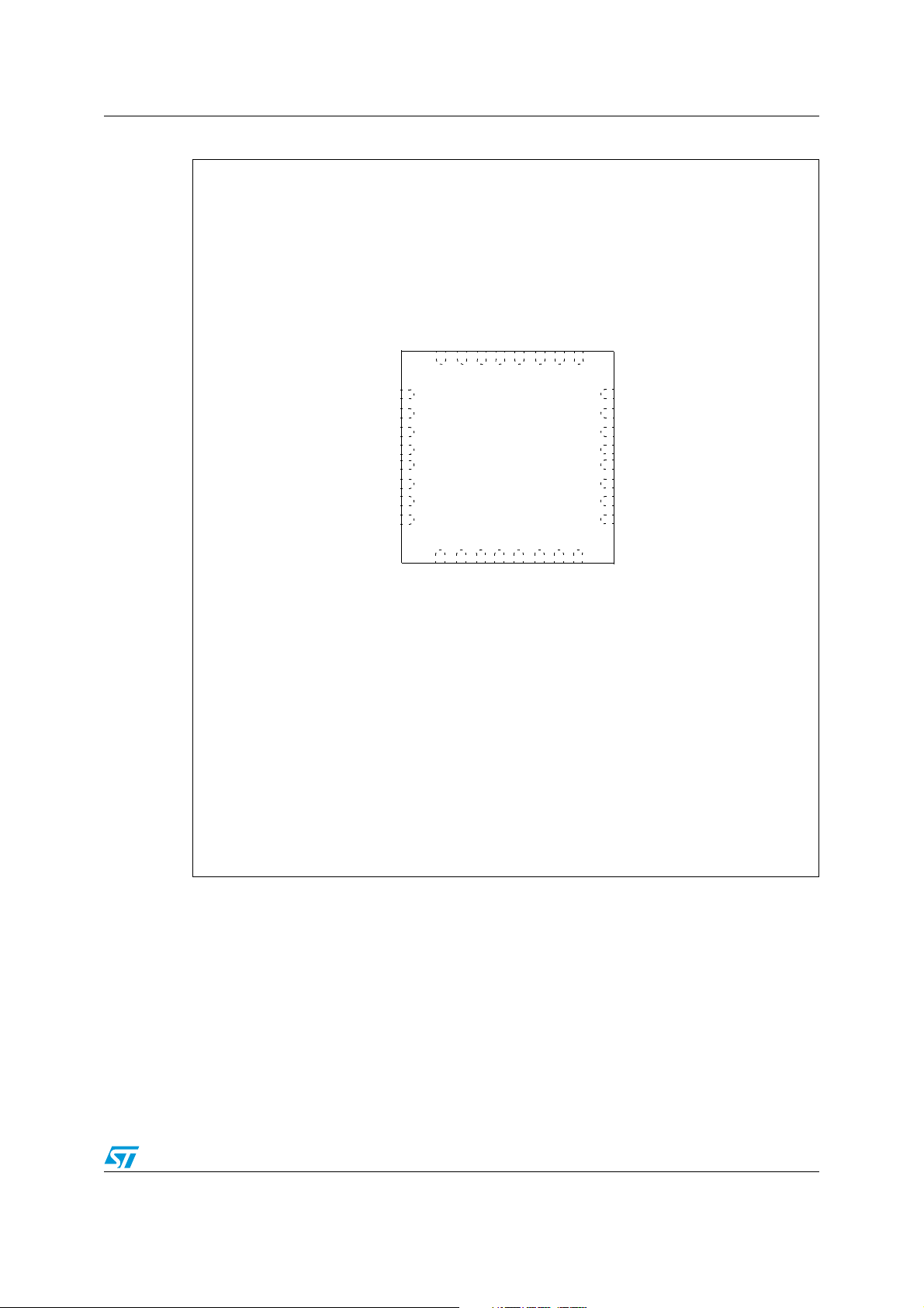
Figure 37. UFQFPN32 - 32-lead ultra thin fine pitch quad flat no-lead package outline (5 x 5). . . . . . 67
Figure 38. UFQFPN32 recommended footprint
Figure 39. LQFP32 - 32-pin low profile quad flat package outline (7 x 7) . . . . . . . . . . . . . . . . . . . . . . 69
Figure 40. LQFP32 recommended footprint
Figure 41. UFQFPN28 - 28-lead ultra thin fine pitch quad flat no-lead package outline (4 x 4)
Figure 42. UFQFPN28 recommended footprint . . . . . . . . . . . . . . . . . . . . . . . . . . . . . . . . . . . . . . . . . . 70
Figure 43. UFQFPN20 3 x 3 mm 0.6 mm package outline . . . . . . . . . . . . . . . . . . . . . . . . . . . . . . . . . 71
Figure 44. UFQFPN20 recommended footprint
Figure 45. TSSOP20 - 20-lead thin shrink small package outline . . . . . . . . . . . . . . . . . . . . . . . . . . . 72
Figure 46. TSSOP20 recommended footprint
. . . . . . . . . . . . . . . . . . . . . . . . . . . . . . . . . . . . . . . . . . . . . . 46
DD
vs. VDD with VIN=VSS. . . . . . . . . . . . . . . . . . . . . . . . . . . . 51
PU
with VIN=VSS. . . . . . . . . . . . . . . . . . . . . . . . . . . . . . . 52
DD
PU
vs. VDD. . . . . . . . . . . . . . . . . . . . . . . . . . . . . . . . . . . . . . 56
pu
(1)
(1)
(1)
. . . . . . . . . . . . . . . . . . . . . . . . . . . . . . . . . . . . . . . . . . . 69
(1)
= 3 V . . . . . . . . . . . . . . . . . . . . . . . . . . . . . . . 47
DD
vs. VDD . . . . . . . . . . . . . . . . . . . . . . . . . . . . . . . . . . 55
(1)
. . . . . . . . . . . . . . . . . . . . . . . . . . . . . . 58
. . . . . . . . . . . . . . . . . . . . . . . . . . . . . . . . . . . . . . . . . 59
. . . . . . . . . . . . . . . . . . . . . . . . . . . . . . . . . . . . . . . . 67
(1)
. . . . . . . . . . . . . . . . . . . . . . . . . . . . . . . . . . . . . . . . 71
. . . . . . . . . . . . . . . . . . . . . . . . . . . . . . . . . . . . . . . . . 72
(1)
. . . . 70
Doc ID 15275 Rev 11 5/81

List of figures STM8L101xx
Figure 47. STM8L101xx ordering information scheme . . . . . . . . . . . . . . . . . . . . . . . . . . . . . . . . . . . . 73
6/81 Doc ID 15275 Rev 11

STM8L101xx Introduction
1 Introduction
This datasheet provides the STM8L101xx pinout, ordering information, mechanical and
electrical device characteristics.
For complete information on the STM8L101xx microcontroller memory, registers and
peripherals, please refer to the STM8L reference manual.
The STM8L101xx devices are members of the STM8L low power 8-bit family. They are
referred to as low-density devices in the STM8L101xx microcontroller family reference
manual (RM0013) and in the STM8L Flash programming manual (PM0054).
All devices of the SM8L product line provide the following benefits:
● Reduced system cost
– Up to 8 Kbytes of low-density embedded Flash program memory including up to
2 Kbytes of data EEPROM
– High system integration level with internal clock oscillators and watchdogs.
– Smaller battery and cheaper power supplies.
● Low power consumption and advanced features
– Up to 16 MIPS at 16 MHz CPU clock frequency
– Less than 150 µA/MH, 0.8 µA in Active-halt mode, and 0.3 µA in Halt mode
– Clock gated system and optimized power management
● Short development cycles
– Application scalability across a common family product architecture with
compatible pinout, memory map and modular peripherals.
– Full documentation and a wide choice of development tools
● Product longevity
– Advanced core and peripherals made in a state-of-the art technology
– Product family operating from 1.65 V to 3.6 V supply
2 Description
The STM8L101xx low power family features the enhanced STM8 CPU core providing
increased processing power (up to 16 MIPS at 16 MHz) while maintaining the advantages of
a CISC architecture with improved code density, a 24-bit linear addressing space and an
optimized architecture for low power operations.
The family includes an integrated debug module with a hardware interface (SWIM) which
allows non-intrusive in-application debugging and ultrafast Flash programming.
All STM8L101xx microcontrollers feature low power low-voltage single-supply program
Flash memory. The 8-Kbyte devices embed data EEPROM.
The STM8L101xx low power family is based on a generic set of state-of-the-art peripherals.
The modular design of the peripheral set allows the same peripherals to be found in different
ST microcontroller families including 32-bit families. This makes any transition to a different
Doc ID 15275 Rev 11 7/81
Description STM8L101xx
family very easy, and simplified even more by the use of a common set of development
tools.
All STM8L low power products are based on the same architecture with the same memory
mapping and a coherent pinout.
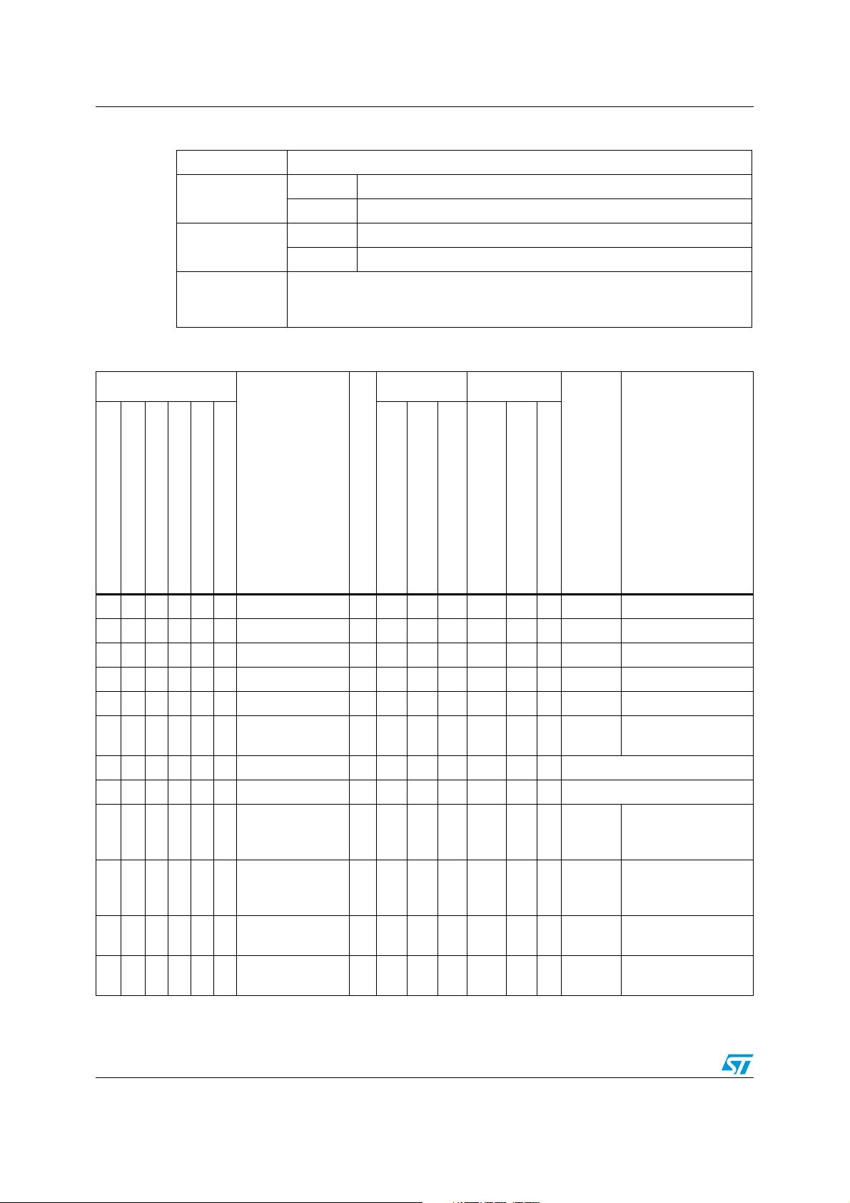
Table 2. Device features
Features STM8L101xx
Flash
2 Kbytes of Flash program
memory
4 Kbytes of Flash program
memory
RAM 1.5 Kbytes
Independent watchdog (IWDG), Auto-wakeup unit (AWU), Beep,
Peripheral functions
Serial peripheral interface (SPI), Inter-integrated circuit (I²C),
Universal synchronous / asynchronous receiver / transmitter (USART),
2 comparators, Infrared (IR) interface
Timers Two 16-bit timers, one 8-bit timer
Operating voltage 1.65 to 3.6 V
Operating temperature -40 to +85 °C
UFQFPN28 4x 4
Packages UFQFPN20 3x3
UFQFPN20 3x3
TSSOP20 4.4 x 6.4
8 Kbytes of Flash program
memory including up to
2 Kbytes of Data EEPROM
-40 to +85 °C or
-40 to +125 °C
UFQFPN28 4x4
UFQFPN20 3x3
UFQFPN32
LQFP32
8/81 Doc ID 15275 Rev 11
STM8L101xx Product overview
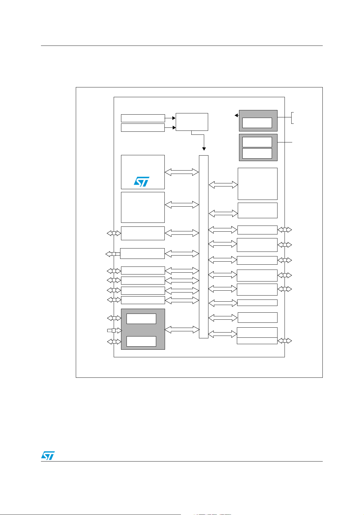
STM8
16 MHz int RC
Clock
controller
Clocks
AWU
Beeper
Address and data bus
38 kHz int RC
Debug module
I²C1
SPI
USART
Up to 8 Kbytes
Flash memory
controller
1.5 Kbytes
to core and
peripherals
IWDG
Core
16-bit Timer 2
(SWIM)
up to 16 MHz
Nested interrupt
up to 29 external
multimaster
8-bit Timer 4
SRAM
interrupts
(including
up to 2 Kbytes
data EEPROM)
Power
Volt. reg.
@V
DD
V
DD18
V
DD
=1.65 V
V
SS
3.6 V
NRST
POR/PDR
to
Reset
COMP1
COMP2
Port A
Port B
Port C
Port D
RX, TX, CK
SDA, SCL
PA[6:0]
PB[7:0]
PC[6:0]
PD[7:0]
MOSI, MISO,
SCK, NSS
BEEP
SWIM
COMP1_CH[4:1]
COMP_REF
Infrared interface
IR_TIM
16-bit Timer 3
TIM2_CH[2:1]
TIM3_CH[2:1]
TIM2_TRIG
TIM3_TRIG
COMP2_CH[4:1]
3 Product overview
Figure 1. STM8L101xx device block diagram
Legend:
AWU: Auto-wakeup unit
Int. RC: internal RC oscillator
I²C: Inter-integrated circuit multimaster interface
POR/PDR: Power on reset / power down reset
SPI: Serial peripheral interface
SWIM: Single wire interface module
USART: Universal synchronous / asynchronous receiver / transmitter
IWDG: Independent watchdog
Doc ID 15275 Rev 11 9/81

Product overview STM8L101xx
3.1 Central processing unit STM8
The 8-bit STM8 core is designed for code efficiency and performance.
It features 21 internal registers, 20 addressing modes including indexed, indirect and relative
addressing, and 80 instructions.
3.2 Development tools
Development tools for the STM8 microcontrollers include:
● The STice emulation system offering tracing and code profiling
● The STVD high-level language debugger including C compiler, assembler and
integrated development environment
● The STVP Flash programming software
The STM8 also comes with starter kits, evaluation boards and low-cost in-circuit
debugging/programming tools.
3.3 Single wire data interface (SWIM) and debug module
The debug module with its single wire data interface (SWIM) permits non-intrusive real-time
in-circuit debugging and fast memory programming.
The Single wire interface is used for direct access to the debugging module and memory
programming. The interface can be activated in all device operation modes.
The non-intrusive debugging module features a performance close to a full-featured
emulator. Beside memory and peripherals, also CPU operation can be monitored in realtime by means of shadow registers.
3.4 Interrupt controller
The STM8L101xx features a nested vectored interrupt controller:
● Nested interrupts with 3 software priority levels
● 26 interrupt vectors with hardware priority
● Up to 29 external interrupt sources on 10 vectors
● Trap and reset interrupts
10/81 Doc ID 15275 Rev 11

STM8L101xx Product overview
3.5 Memory
The STM8L101xx devices have the following main features:
● 1.5 Kbytes of RAM
● The EEPROM is divided into two memory arrays (see the STM8L reference manual for
details on the memory mapping):
– Up to 8 Kbytes of low-density embedded Flash program including up to 2 Kbytes
of data EEPROM. Data EEPROM and Flash program areas can be write protected
independently by using the memory access security mechanism (MASS).
– 64 option bytes (one block) of which 5 bytes are already used for the device.
Error correction code is implemented on the EEPROM.
3.6 Low power modes
To minimize power consumption, the product features three low power modes:
● Wait mode: CPU clock stopped, selected peripherals at full clock speed.
● Active-halt mode: CPU and peripheral clocks are stopped. The programmable wakeup
time is controlled by the AWU unit.
● Halt mode: CPU and peripheral clocks are stopped, the device remains powered on.
Wakeup is triggered by an external interrupt.
3.7 Voltage regulators
The STM8L101xx embeds an internal voltage regulator for generating the 1.8 V power
supply for the core and peripherals.
This regulator has two different modes: main voltage regulator mode (MVR) and low power
voltage regulator mode (LPVR). When entering Halt or Active-halt modes, the system
automatically switches from the MVR to the LPVR in order to reduce current consumption.
3.8 Clock control
The STM8L101xx embeds a robust clock controller. It is used to distribute the system clock
to the core and the peripherals and to manage clock gating for low power modes. This
system clock is a 16-MHz High Speed Internal RC oscillator (HSI RC), followed by a
programmable prescaler.
In addition, a 38 kHz low speed internal RC oscillator is used by the independent watchdog
(IWDG) and Auto-wakeup unit (AWU).
3.9 Independent watchdog
The independent watchdog (IWDG) peripheral can be used to resolve processor
malfunctions due to hardware or software failures.
It is clocked by the 38 kHZ LSI internal RC clock source, and thus stays active even in case
of a CPU clock failure.
Doc ID 15275 Rev 11 11/81

Product overview STM8L101xx
3.10 Auto-wakeup counter
The auto-wakeup (AWU) counter is used to wakeup the device from Active-halt mode.
3.11 General purpose and basic timers
STM8L101xx devices contain two 16-bit general purpose timers (TIM2 and TIM3) and one
8-bit basic timer (TIM4).
16-bit general purpose timers
The 16-bit timers consist of 16-bit up/down auto-reload counters driven by a programmable
prescaler. They perform a wide range of functions, including:
● Time base generation
● Measuring the pulse lengths of input signals (input capture)
● Generating output waveforms (output compare, PWM and One pulse mode)
● Interrupt capability on various events (capture, compare, overflow, break, trigger)
● Synchronization with other timers or external signals (external clock, reset, trigger and
enable)
8-bit basic timer
The 8-bit timer consists of an 8-bit up auto-reload counter driven by a programmable
prescaler. It can be used for timebase generation with interrupt generation on timer overflow.
3.12 Beeper
The STM8L101xx devices include a beeper function used to generate a beep signal in the
range of 1, 2 or 4 kHz when the LSI clock is operating at a frequency of 38 kHz.
3.13 Infrared (IR) interface
The STM8L101xx devices contain an infrared interface which can be used with an IR LED
for remote control functions. Two timer output compare channels are used to generate the
infrared remote control signals.
3.14 Comparators
The STM8L101xx features two zero-crossing comparators (COMP1 and COMP2) sharing
the same current bias and voltage reference. The voltage reference can be internal
(comparison with ground) or external (comparison to a reference pin voltage).
Each comparator is connected to 4 channels, which can be used to generate interrupt, timer
input capture or timer break. Their polarity can be inverted.
12/81 Doc ID 15275 Rev 11

STM8L101xx Product overview
3.15 USART
The USART interface (USART) allows full duplex, asynchronous communications with
external devices requiring an industry standard NRZ asynchronous serial data format. It
offers a very wide range of baud rates.
3.16 SPI
The serial peripheral interface (SPI) provides half/ full duplex synchronous serial
communication with external devices. It can be configured as the master and in this case it
provides the communication clock (SCK) to the external slave device. The interface can also
operate in multi-master configuration.
3.17 I²C
The inter-integrated circuit (I2C) bus interface is designed to serve as an interface between
the microcontroller and the serial I
2
C bus. It provides multi-master capability, and controls all
I²C bus-specific sequencing, protocol, arbitration and timing. It manages standard and fast
speed modes.
Doc ID 15275 Rev 11 13/81
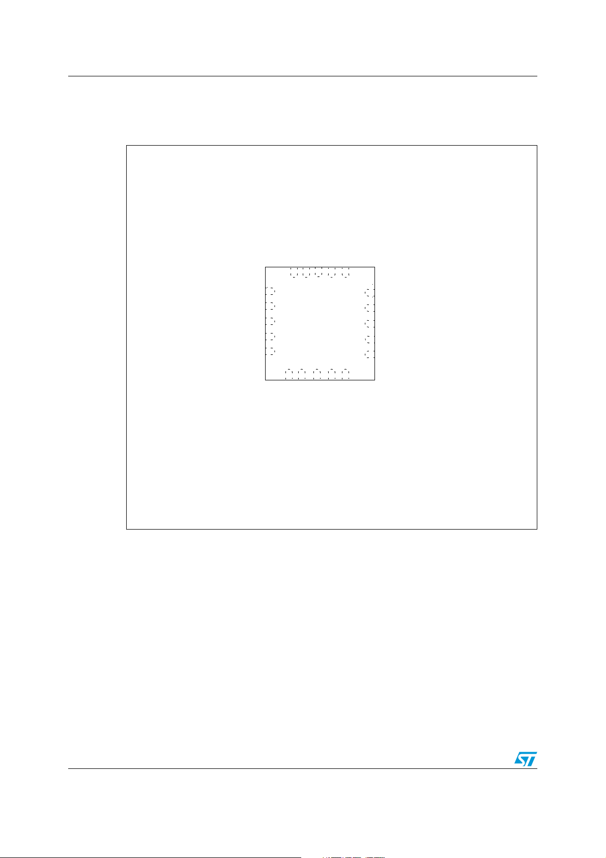
Pin description STM8L101xx
2
1
3
4
5
67 8
9
11
12
13
14
15
16171819
PD0 (HS) / TIM3_CH2 / COMP1_CH3
V
DD
V
SS
PA3 (HS)
PA2 (HS)
PB0 (HS) / TIM2_CH1 / COMP1_CH1
NRST / PA1 (HS)
PC3 (HS) / USART_TX
PC4 (HS) / USART_CK / CCO
PC2 (HS) / USART_RX
PC1 / I²C_SCL
PB4 (HS) / SPI_NSS
PB5 (HS) / SPI_SCK
PB6 (HS) / SPI_MOSI
PB7 (HS) / SPI_MISO
PC0 / I²C_SDA
PB1 (HS) / TIM3_CH1 /COMP1_CH2
PB2 (HS) / TIM2_CH2 / COMP2_CH1
10
PB3 (HS) / TIM2_TRIG / COMP2_CH2
PA0 (HS) / SWIM / BEEP / IR_TIM
20
4 Pin description
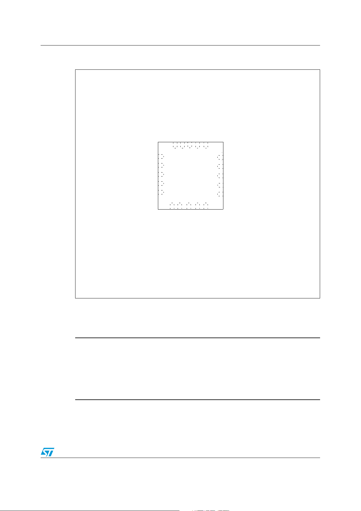
Figure 2. Standard 20-pin UFQFPN package pinout
1. HS corresponds to 20 mA high sink/source capability.
2. High sink LED driver capability available on PA0. Refer to the description of the IR_CR register in the
STM8L reference manual (RM0013).
Note: The COMP_REF pin is not available in this standard 20-pin UFQFPN package. It is available
on Port A6 in the 20-pin UFQFPN package pinout for STM8L101F1U6ATR,
STM8L101F2U6ATR and STM8L101F3U6ATR part numbers (Figure 3 on page 15).
14/81 Doc ID 15275 Rev 11
STM8L101xx Pin description
2
1
3
4
5
67 8
9
11
12
13
14
15
16171819
PD0 (HS) / TIM3_CH2 / COMP1_CH3
V
DD
V
SS
PA6 (HS) / COMP_REF
PA2 (HS)
PB0 (HS) / TIM2_CH1 / COMP1_CH1
NRST / PA1 (HS)
PC3 (HS) / USART_TX
PC4 (HS) / USART_CK / CCO
PC2 (HS) / USART_RX
PC1 / I²C_SCL
PB4 (HS) / SPI_NSS
PB5 (HS) / SPI_SCK
PB6 (HS) / SPI_MOSI
PB7 (HS) / SPI_MISO
PC0 / I²C_SDA
PB1 (HS) / TIM3_CH1 /COMP1_CH2
PB2 (HS) / TIM2_CH2 / COMP2_CH1
10
PB3 (HS) / TIM2_TRIG / COMP2_CH2
PA0 (HS) / SWIM / BEEP / IR_TIM
20
Figure 3. 20-pin UFQFPN package pinout for STM8L101F1U6ATR,
STM8L101F2U6ATR and STM8L101F3U6ATR part numbers
1. Please refer to the warning below.
2. HS corresponds to 20 mA high sink/source capability.
3. High sink LED driver capability available on PA0. Refer to the description of the IR_CR register in the
STM8L reference manual (RM0013).
Warning: For the STM8L101F1U6ATR, STM8L101F2U6ATR and
STM8L101F3U6ATR part numbers (devices with COMP_REF
pin), all ports available on 32-pin packages must be
considered as active ports. To avoid spurious effects, you
have to configure them as input pull-up. A small increase in
consumption (typ. < 300 µA) may occur during the power up
and reset phase until these ports are properly configured.
Doc ID 15275 Rev 11 15/81
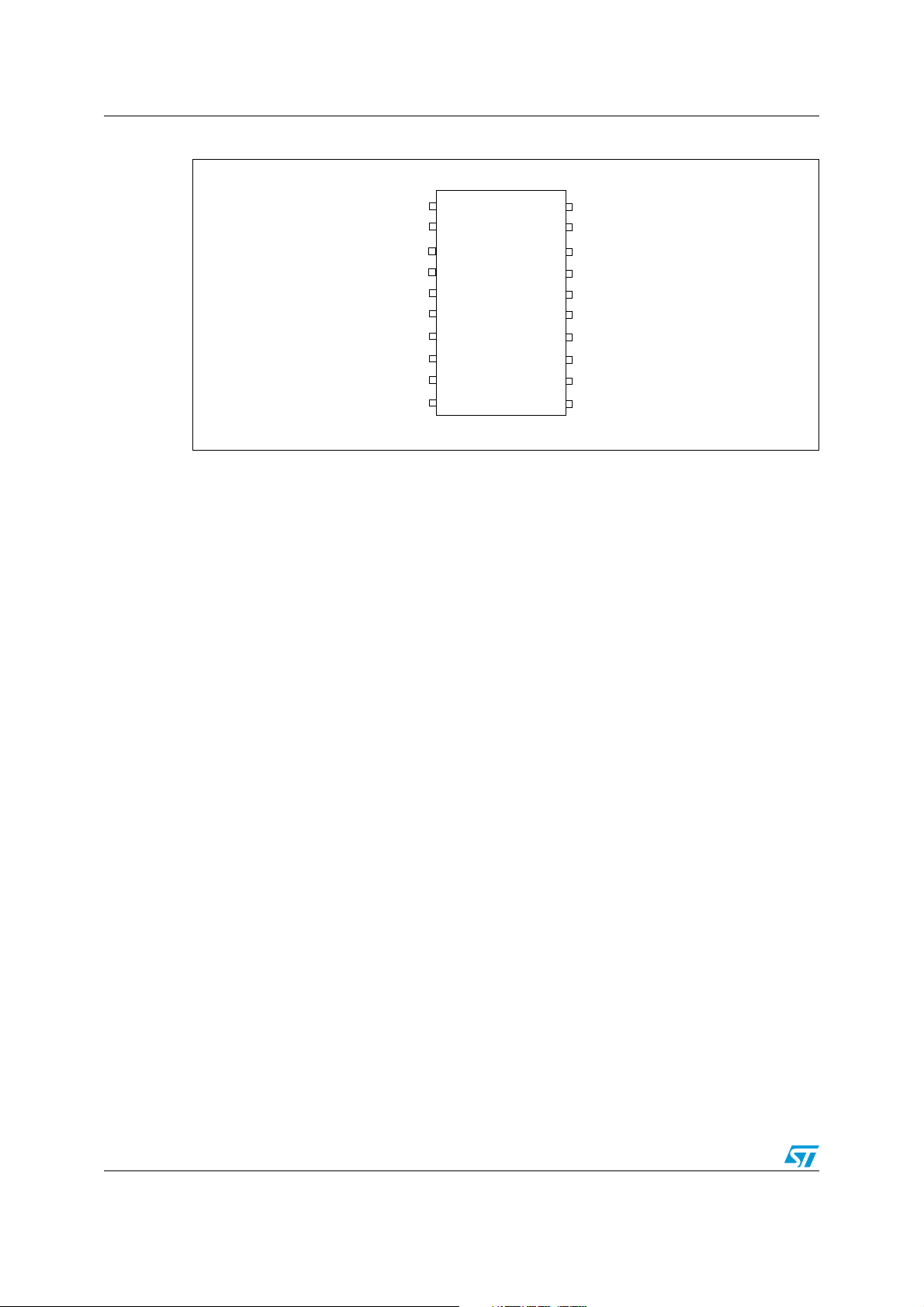
Pin description STM8L101xx
PA 3 ( H S )
PA 2 ( HS )
NRST / PA1 (HS)
PA0 (HS) / SWIM / BEEP / IR_TIM
PC4 (HS) / USART_CK/ CCO
V
SS
PC3 (HS) / USART_TX
PC0 / I²C_SDA
PC1 / I²C_SCL
PB7 (HS) / SPI_MISO
PB6 (HS) / SPI_MOSI
PB1 (HS) / TIM3_CH1 / COMP1_CH2
PB2 (HS) / TIM2_CH2 / COMP2_CH1
PB3 (HS) /TIM2_TRIG /COMP2_CH2
PB4 (HS) / SPI_NSS
PB5 (HS) / SPI_SCK
V
DD
PD0 (HS) / TIM3_CH2 / COMP1_CH3
PB0 (HS) / TIM2_CH1 / COMP1_CH1
PC2 (HS) / USART_RX
1
2
3
4
5
6
7
10
9
8
20
19
18
17
16
15
14
11
12
13
Figure 4. 20-pin TSSOP package pinout
1. HS corresponds to 20 mA high sink/source capability.
2. High sink LED driver capability available on PA0. Refer to the description of the IR_CR register in the
STM8L reference manual (RM0013).
16/81 Doc ID 15275 Rev 11
STM8L101xx Pin description
PD3
(HS) / COMP2_CH4
PB0 (HS) / TIM2_CH1 / COMP1_CH1
PB1 (HS) / TIM3_CH1 / COMP1_CH2
PB2 (HS) / TIM2_CH2 / COMP2_CH1
PD0 (HS) / TIM3_CH2 / COMP1_CH3
PD1 (HS) / TIM3_TRIG / COMP1_CH4
PD2(HS) / COMP2_CH3
PA5 (HS) / TIM3_BKIN
V
SS
V
DD
NRST / PA1 (HS)
PA2 ( H S )
PA3 (HS)
PA4 (HS) / TIM2_BKIN
PB6 (HS) / SPI_MOSI
PB5 (HS) / SPI_SCK
PB4 (HS) / SPI_NSS
PB3 (HS) / TIM2_TRIG / COMP2_CH2
PC0 / I²C_SDA
PD4 (HS)
PB7 (HS) / SPI_MISO
PC4 (HS) / USART_CK / CCO
PC3 (HS) / USART_TX
PC2 (HS) / USART_RX
PC1 / I²C_SCL
PA0 (HS) / SWIM / BEEP / IR_TIM
PC6 (HS)
PC5 (HS)
2
1
3
4
5
6
7
98 10 11 12 13 14
20
21
19
18
17
16
15
2728 26 25 24 23 22
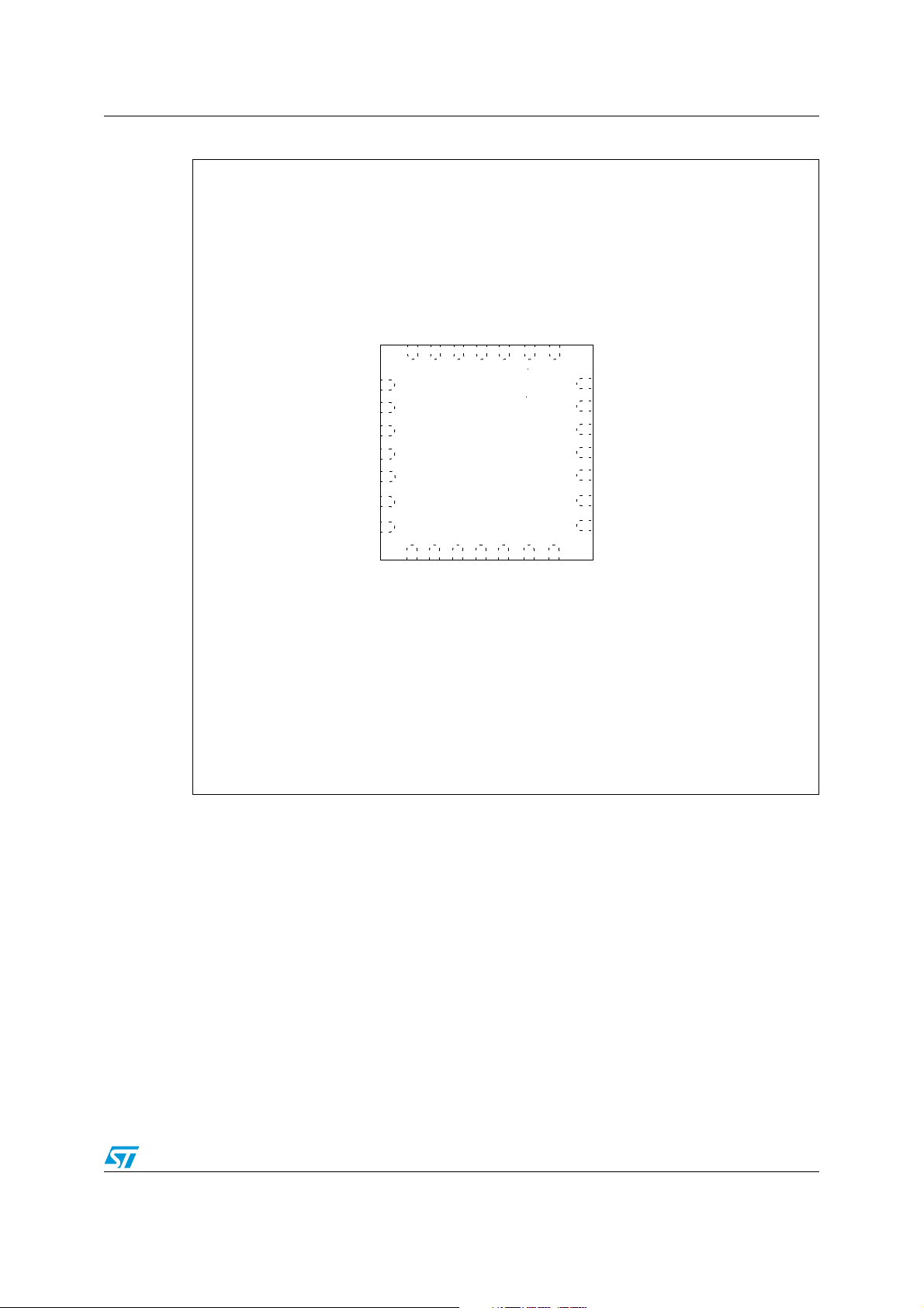
Figure 5. Standard 28-pin UFQFPN package pinout
1. HS corresponds to 20 mA high sink/source capability.
2. High sink LED driver capability available on PA0. Refer to the description of the IR_CR register in the
STM8L reference manual (RM0013).
Note: The COMP_REF pin is not available in this standard 28-pin UFQFPN package. It is available
on Port A6 in the 28-pin UFQFPN package pinout for STM8L101G3U6ATR and
STM8L101G2U6ATR part numbers (Figure 6 on page 18).
Doc ID 15275 Rev 11 17/81
Pin description STM8L101xx
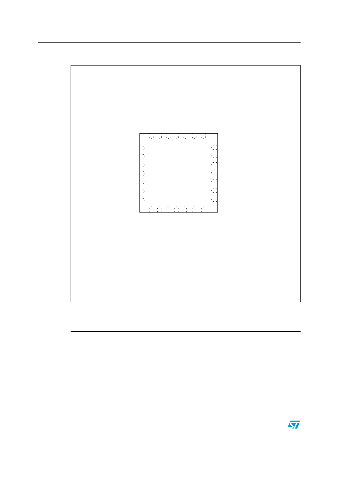
PD3(HS) / COMP2_CH4
PB0 (HS) / TIM2_CH1 / COMP1_CH1
PB1 (HS) / TIM3_CH1 / COMP1_CH2
PB2 (HS) / TIM2_CH2 / COMP2_CH1
PD0 (HS) / TIM3_CH2 / COMP1_CH3
PD1 (HS) / TIM3_TRIG / COMP1_CH4
PD2(HS) / COMP2_CH3
PA6 (HS) / COMP_REF
V
SS
V
DD
NRST / PA1 (HS)
PA2 ( H S )
PA3 (HS)
PA4 (HS) / TIM2_BKIN
PB6 (HS) / SPI_MOSI
PB5 (HS) / SPI_SCK
PB4 (HS) / SPI_NSS
PB3 (HS) / TIM2_TRIG / COMP2_CH2
PC0 / I²C_SDA
PD4 (HS)
PB7 (HS) / SPI_MISO
PC4 (HS) / USART_CK / CCO
PC3 (HS) / USART_TX
PC2 (HS) / USART_RX
PC1 / I²C_SCL
PA0 (HS) / SWIM / BEEP / IR_TIM
PC6 (HS)
PC5 (HS)
2
1
3
4
5
6
7
98 10 11 12 13 14
20
21
19
18
17
16
15
2728 26 25 24 23 22
Figure 6. 28-pin UFQFPN package pinout for STM8L101G3U6ATR and
STM8L101G2U6ATR part numbers
1. HS corresponds to 20 mA high sink/source capability.
2. High sink LED driver capability available on PA0. Refer to the description of the IR_CR register in the
STM8L reference manual (RM0013).
Warning: For the STM8L101G3U6ATR and STM8L101G2U6ATR part
numbers (devices with COMP_REF pin), all ports available on
32-pin packages must be considered as active ports. To avoid
spurious effects, you have to configure them as input pull-up.
A small increase in consumption (typ. < 300 µA) may occur
during the power up and reset phase until these ports are
properly configured.
18/81 Doc ID 15275 Rev 11
STM8L101xx Pin description
1
2
3
4
PA5 (HS) / TIM3_BKIN
PA6 (HS) / COMP_REF
V
SS
V
DD
NRST / PA1 (HS)
PA2 (HS)
PA3 (HS)
PA4 (HS) / TIM2_BKIN
PD1 (HS) / TIM3_TRIG / COMP1_CH4
PD2 (HS) / / COMP2_CH3
PD3 (HS) / COMP2_CH4
PB0 (HS) / TIM2_CH1 / COMP1_CH1
PB1 (HS) / TIM3_CH1 / COMP1_CH2
PB2 (HS) / TIM2_CH2 / COMP2_CH1
PB3 (HS) / TIM2_TRIG / COMP2_CH2
PD0 (HS) / TIM3_CH2 / COMP1_CH3
PD7 (HS)
PD6 (HS)
PB4 (HS) / SPI_NSS
PB5 (HS) / SPI_SCK
PB7 (HS) / SPI_MISO
PD5 (HS)
PD4 (HS)
PB6 (HS) / SPI_MOSI
PC3 (HS) / USART_TX
PC2 (HS) / USART_RX
PC1 / I²C_SCL
PC0 / I²C_SDA
PA0 (HS) / SWIM / BEEP / IR_TIM
PC6 (HS)
PC5 (HS)
PC4 (HS) / USART_CK / CCO
5
6
7
8
910111213 14 15 16
17
18
19
20
21
22
23
24
32 31 30 29
28 27 26 25
Figure 7. 32-pin package pinout
1. Example given for the UFQFPN32 package. The pinout is the same for the LQFP32 package.
2. HS corresponds to 20 mA high sink/source capability.
3. High sink LED driver capability available on PA0. Refer to the description of the IR_CR register in the
STM8L reference manual (RM0013).
Doc ID 15275 Rev 11 19/81
Pin description STM8L101xx
Table 3. Legend/abbreviation for table 4
Typ e I= input, O = output, S = power supply
Level
Input CM = CMOS
Output HS = high sink/source (20 mA)
Port and control
configuration
Input float = floating, wpu = weak pull-up
Output T = true open drain, OD = open drain, PP = push pull
Bold X (pin state after reset release).
Reset state
Unless otherwise specified, the pin state is the same during the reset phase (i.e.
“under reset”) and after internal reset release (i.e. at reset state).
(1)
TSSOP20
UFQFPN20 with COMP_REF
standard UFQFPN28
(1)
UFQFPN32 or LQFP32
UFQFPN28 with COMP_REF
Pin name
(2)
Input Output
Typ e
wpu
floating
OD
PP
Main function
Alternate function
(after reset)
Ext. interrupt
High sink/source
I/O X HS X X Reset PA 1
Table 4. STM8L101xx pin description
Pin number
standard UFQFPN20
1 14111NRST/PA1
2 25222PA2 I/OX XXHSXXPort A2
3 - 6333PA3 I/OX XXHSXXPort A3
- - - 4 4 4 PA4/TIM2_BKIN I/O X XXHSXXPort A4 Timer 2 - break input
- - - 5 - 5 PA5/TIM3_BKIN I/O X XXHSXXPort A5 Timer 3 - break input
- 3 - - 5 6 PA6/COMP_REF I/O X XXHSXXPort A6
4 47667V
5 58778V
6 69889
---9910
---101011
---111112
SS
DD
PD0/TIM3_CH2/
COMP1_CH3
PD1/TIM3_TRIG/
COMP1_CH4
PD2/
COMP2_CH3
PD3/
COMP2_CH4
S Ground
S Power supply
I/O X XXHSXXPort D0
I/O X XXHSXXPort D1
I/O X XXHSXXPort D2
I/O X XXHSXXPort D3
Comparator external
reference
Timer 3 - channel 2 /
Comparator 1 channel 3
Timer 3 - trigger /
Comparator 1 channel 4
Comparator 2 channel 3
Comparator 2 channel 4
20/81 Doc ID 15275 Rev 11

STM8L101xx Pin description
Table 4. STM8L101xx pin description (continued)
Pin number
(1)
(1)
TSSOP20
standard UFQFPN20
UFQFPN20 with COMP_REF
standard UFQFPN28
UFQFPN28 with COMP_REF
7 7 10 12 12 13
8 8 11 13 13 14
9 9 12 14 14 15
10 10 13 15 15 16
Pin name
UFQFPN32 or LQFP32
PB0/TIM2_CH1/
COMP1_CH1
PB1/TIM3_CH1/
COMP1_CH2
PB2/ TIM2_CH2/
COMP2_CH1/
PB3/TIM2_TRIG/
COMP2_CH2
Input Output
Typ e
wpu
floating
OD
Ext. interrupt
High sink/source
(3)
I/O X
XHSX XPort B0
(3)X(3)
I/O X XXHSXXPort B1
I/O X XXHSXXPort B2
I/O X XXHSXXPort B3
PP
Main function
Alternate function
(after reset)
Timer 2 - channel 1 /
Comparator 1 channel 1
Timer 3 - channel 1 /
Comparator 1 channel 2
Timer 2 - channel 2 /
Comparator 2 channel 1
Timer 2 - trigger /
Comparator 2 channel 2
11 11 14 16 16 17 PB4/SPI_NSS
(3)
I/O X
(3)X(3)
XHSX XPort B4
SPI master/slave
select
12 12 15 17 17 18 PB5/SPI_SCK I/O X XXHSXXPort B5 SPI clock
13 13 16 18 18 19 PB6/SPI_MOSI I/O X XXHSXXPort B6
14 14 17 19 19 20 PB7/SPI_MISO I/O X XXHSXXPort B7
SPI master out/ slave
in
SPI master in/ slave
out
- - - 202021PD4 I/O X XXHSXXPor t D4
- ----22PD5 I/OX XXHSXXPort D5
- ----23PD6 I/OX XXHSXXPort D6
- ----24PD7 I/OX XXHSXXPort D7
15 15 18 21 21 25 PC0/I2C_SDA I/O X XT
16 16 19 22 22 26 PC1/I2C_SCL I/O X XT
(4)
(4)
Port C0 I2C data
Port C1 I2C clock
17 17 20 23 23 27 PC2/USART_RX I/O X XXHSXXPort C2 USART receive
18 18 1 24 24 28 PC3/USART_TX I/O X XXHSXXPort C3 USART transmit
19 19 2 25 25 29
PC4/USART_CK/
CCO
I/O X XXHSXXPort C4
USART synchronous
clock / Configurable
clock output
- - - 262630PC5 I/O X XXHSXXPor t C5
Doc ID 15275 Rev 11 21/81
Pin description STM8L101xx
Table 4. STM8L101xx pin description (continued)
Pin number
(1)
TSSOP20
standard UFQFPN20
UFQFPN20 with COMP_REF
(1)
standard UFQFPN28
UFQFPN32 or LQFP32
UFQFPN28 with COMP_REF
Pin name
Input Output
Typ e
wpu
floating
OD
Ext. interrupt
High sink/source
PP
Main function
Alternate function
(after reset)
- - - 272731PC6 I/O X XXHSXXPor t C6
SWIM input and output /Beep output/Timer Infrared
20 20 3 28 28 32
(5)
/SWIM/
PA 0
BEEP/IR_TIM
(6)
I/O X X
(5)
XHS
(6)
XXPort A0
output
1. Please refer to the warning below.
2. At power-up, the PA1/NRST pin is a reset input pin with pull-up. To be used as a general purpose pin (PA1), it can be
configured only as output open-drain or push-pull, not as a general purpose input. Refer to Section Configuring NRST/PA1
pin as general purpose output in the STM8L101xx reference manual (RM0013).
3. A pull-up is applied to PB0 and PB4 during the reset phase. These two pins are input floating after reset release.
4. In the open-drain output column, ‘T’ defines a true open-drain I/O (P-buffer and protection diode to V
implemented).
5. The PA0 pin is in input pull-up during the reset phase and after reset release.
6. High sink LED driver capability available on PA0.
are not
DD
Warning: For the STM8L101F1U6ATR, STM8L101F2U6ATR,
STM8L101F3U6ATR, STM8L101G2U6ATR and
STM8L101G3U6ATR part numbers (devices with COMP_REF
pin), all ports available on 32-pin packages must be
considered as active ports. To avoid spurious effects, you
have to configure them as input pull-up. A small increase in
consumption (typ. < 300 µA) may occur during the power up
and reset phase until these ports are properly configured.
22/81 Doc ID 15275 Rev 11
STM8L101xx Memory and register map
GPIO and peripheral registers
(2)
0x00 0000
Reserved
Flash program memory
(up to 8 Kbytes)
(1)
Interrupt vectors
0x00 4800
0x00 48FF
RAM
0x00 05FF
(1.5 Kbytes)
(1)
(up to 513 bytes)
(1)
0x 004900
Option bytes
0x00 5000
0x00 57FF
0x00 5800
0x00 7FFF
0x00 8000
0x00 9FFF
0x00 0600
0x00 47FF
0x00 49FF
0x00 7EFF
0x00 8080
0x00 807F
CPU/SWIM/Debug/ITC
Registers
0x00 7F00
Reserved
Reserved
including
Stack
including
Data EEPROM
(up to 2 Kbytes)
0x 004925
0x 004931
0x 004924
0x 004930
Unique ID
Reserved
Low-density
5 Memory and register map
Figure 8. Memory map
1. Table 5 lists the boundary addresses for each memory size. The top of the stack is at the RAM end
address.
2. Refer to Table 7 for an overview of hardware register mapping, to Table 6 for details on I/O port hardware
registers, and to Ta b le 8 for information on CPU/SWIM/debug module controller registers.
Doc ID 15275 Rev 11 23/81
Memory and register map STM8L101xx
Table 5. Flash and RAM boundary addresses
Memory area Size Start address End address
RAM 1.5 Kbytes 0x00 0000 0x00 05FF
2 Kbytes 0x00 8000 0x00 87FF
Flash program memory
Table 6. I/O Port hardware register map
4 Kbytes 0x00 8000 0x00 8FFF
8 Kbytes 0x00 8000 0x00 9FFF
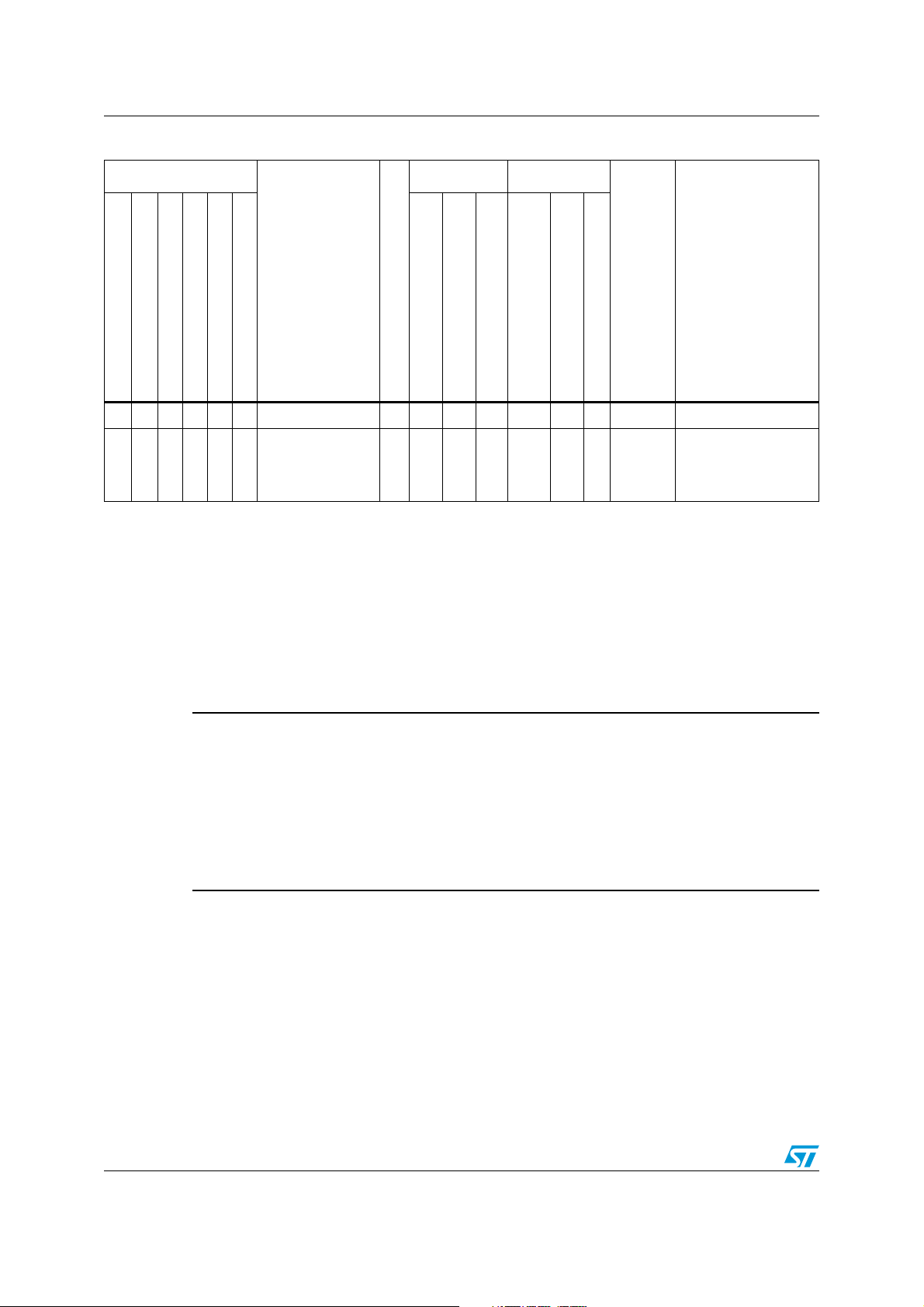
Address Block Register label Register name
0x00 5000
PA_ODR Port A data output latch register 0x00
Reset
status
0x00 5001 PA_IDR Port A input pin value register 0xxx
0x00 5002 PA_DDR Port A data direction register 0x00
Por t A
0x00 5003 PA_CR1 Port A control register 1 0x00
0x00 5004 PA_CR2 Port A control register 2 0x00
0x00 5005
PB_ODR Port B data output latch register 0x00
0x00 5006 PB_IDR Port B input pin value register 0xxx
0x00 5007 PB_DDR Port B data direction register 0x00
Por t B
0x00 5008 PB_CR1 Port B control register 1 0x00
0x00 5009 PB_CR2 Port B control register 2 0x00
0x00 500A
PC_ODR Port C data output latch register 0x00
0x00 500B PC_IDR Port C input pin value register 0xxx
0x00 500C PC_DDR Port C data direction register 0x00
Por t C
0x00 500D PC_CR1 Port C control register 1 0x00
0x00 500E PC_CR2 Port C control register 2 0x00
0x00 500F
PD_ODR Port D data output latch register 0x00
0x00 5010 PD_IDR Port D input pin value register 0xxx
0x00 5011 PD_DDR Port D data direction register 0x00
Por t D
0x00 5012 PD_CR1 Port D control register 1 0x00
0x00 5013 PD_CR2 Port D control register 2 0x00
24/81 Doc ID 15275 Rev 11
STM8L101xx Memory and register map
Table 7. General hardware register map
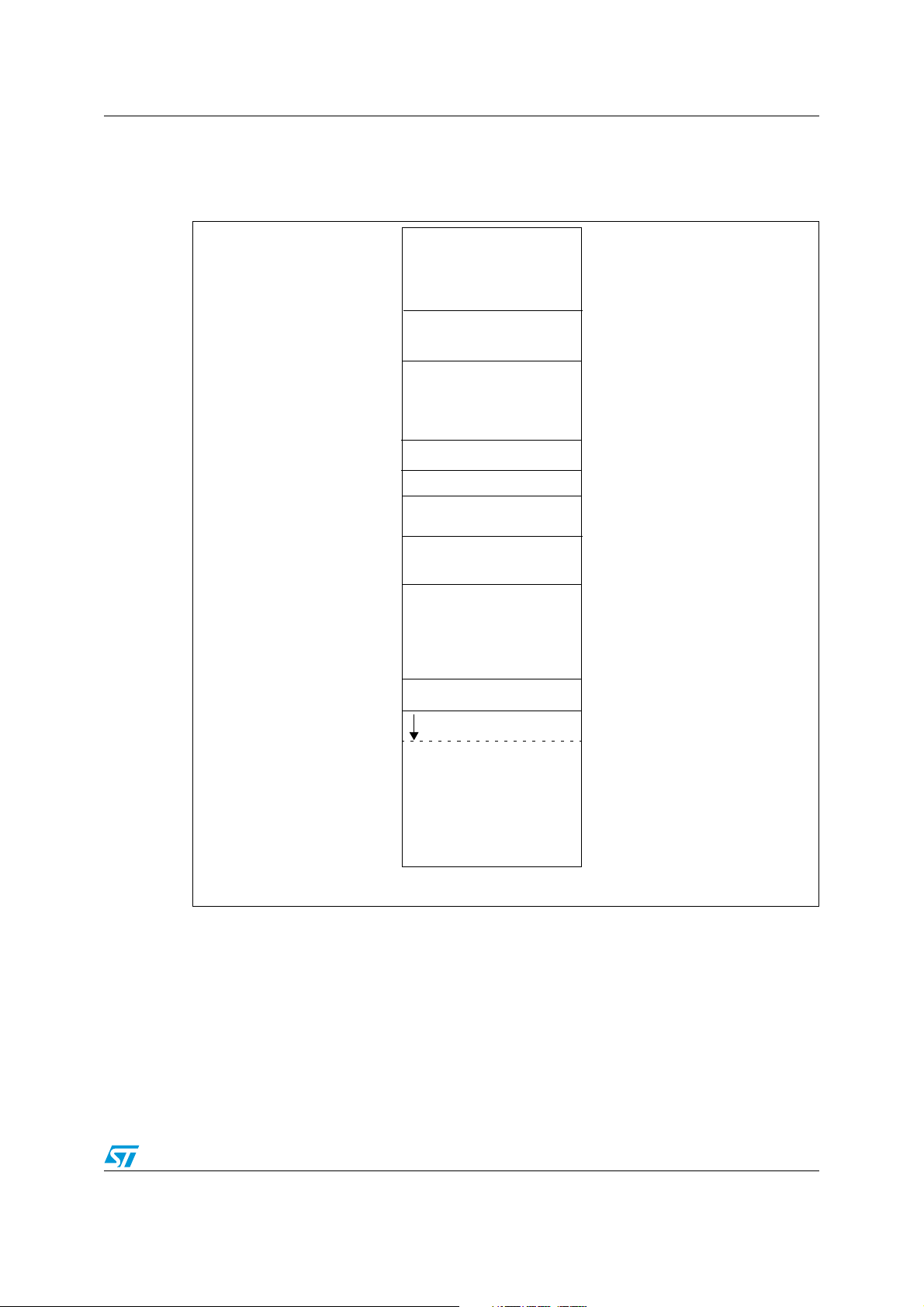
Address Block Register label Register name
0x00 5050
FLASH_CR1 Flash control register 1 0x00
Reset
status
0x00 5051 FLASH_CR2 Flash control register 2 0x00
0x00 5052 FLASH _PUKR
Flash
Flash Program memory unprotection
register
0x00
0x00 5053 FLASH _DUKR Data EEPROM unprotection register 0x00
0x00 5054 FLASH _IAPSR
Flash in-application programming status
register
0xX0
0x00 5055
to
Reserved area (75 bytes)
0x00 509F
0x00 50A0
EXTI_CR1 External interrupt control register 1 0x00
0x00 50A1 EXTI_CR2 External interrupt control register 2 0x00
0x00 50A2 EXTI_CR3 External interrupt control register 3 0x00
ITC-EXTI
0x00 50A3 EXTI_SR1 External interrupt status register 1 0x00
0x00 50A4 EXTI_SR2 External interrupt status register 2 0x00
0x00 50A5 EXTI_CONF External interrupt port select register 0x00
0x00 50A6
WFE_CR1 WFE control register 1 0x00
WFE
0x00 50A7 WFE_CR2 WFE control register 2 0x00
0x00 50A8
to
Reserved area (8 bytes)
0x00 50AF
0x00 50B0
RST_CR Reset control register 0x00
RST
0x00 50B1 RST_SR Reset status register 0x01
0x00 50B2
to
Reserved area (14 bytes)
0x00 50BF
0x00 50C0
CLK_CKDIVR Clock divider register 0x03
0x00 50C1
to
0x00 50C2
CLK
Reserved area (2 bytes)
0x00 50C3 CLK_PCKENR Peripheral clock gating register 0x00
0x00 50C4 Reserved (1 byte)
0x00 50C5 CLK_CCOR Configurable clock control register 0x00
0x00 50C6
to
0x00 50DF
Reserved area (25 bytes)
Doc ID 15275 Rev 11 25/81
 Loading...