

Page 1
High-performance, 802.15.4 wireless system-on-chip
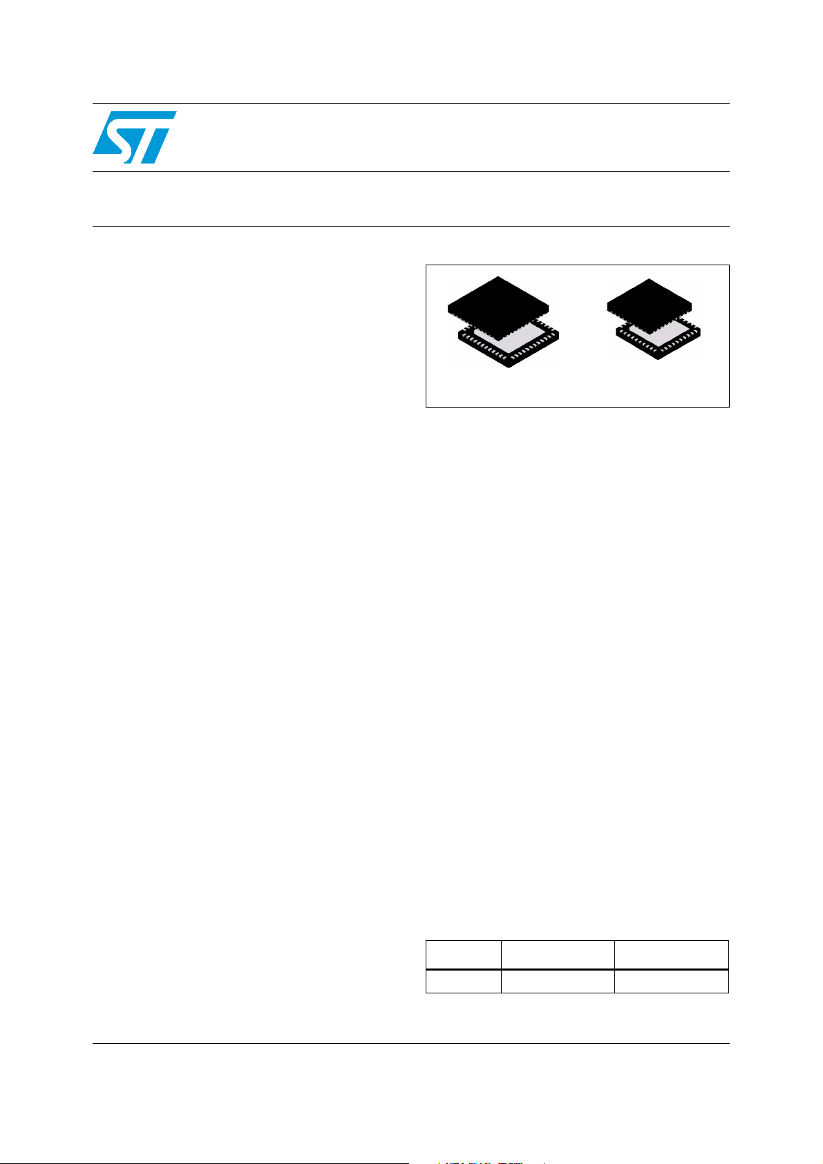
VFQFPN48
VFQFPN40
(6 x 6 mm)
(7 x 7 mm)
Features
■ Complete System-on-Chip
– 32-bit ARM® Cortex™-M3 processor
– 2.4 GHz IEEE 802.15.4 transceiver & lower
MAC
– 128-Kbyte Flash, 8-Kbyte RAM memory
– AES128 encryption accelerator
– Flexible ADC, SPI/UART/TWI serial
communications, and general-purpose
timers
– 24 highly configurable GPIOs with Schmitt
trigger inputs
■ Industry-leading ARM® Cortex™-M3
processor
– Leading 32-bit processing performance
– Highly efficient Thumb®-2 instruction set
– Operation at 6, 12 or 24 MHz
– Flexible nested vectored interrupt controller
■ Low power consumption, advanced
management
– RX Current (w/ CPU): 27 mA
– TX Current (w/ CPU, +3 dBm TX): 31 mA
– Low deep sleep current, with retained RAM
and GPIO: 400 nA/800 nA with/without
sleep timer
– Low-frequency internal RC oscillator for
low-power sleep timing
– High-frequency internal RC oscillator for
fast (100 µs) processor start-up from sleep
■ Exceptional RF performance
– Normal mode link budget up to 102 dB;
configurable up to 107 dB
– -99 dBm normal RX sensitivity;
configurable to -100 dBm (1% PER, 20
byte packet)
– +3 dB normal mode output power;
configurable up to +7 dBm
– Robust WiFi and Bluetooth coexistence
STM32W108HB
STM32W108CB
Data brief
■ Innovative network and processor debug
– Non-intrusive hardware packet trace
– Serial wire/JTAG interface
– Standard ARM debug capabilities: Flash
patch & breakpoint; data watchpoint &
trace; instrumentation trace macrocell
■ Application flexibility
– Single voltage operation: 2.1-3.6 V with
internal 1.8 V and 1.25 V regulators
– Optional 32.768 kHz crystal for higher timer
accuracy
– Low external component count with single
24 MHz crystal
– Support for external power amplifier
– Small 7x7 mm 48-pin QFN package or
6x6 mm 40-pin QFN package
Applications
■ Smart energy
■ Building automation and control
■ Home automation and control
■ Security and monitoring
■ ZigBee® Pro wireless sensor networking
■ RF4CE products and remote controls
■ 6LoWPAN and custom protocols
Table 1. Device summary
Feature STM32W108HB STM32W108CB
Package 40-pin QFN 48-pin QFN
August 2009 Doc ID 15851 Rev 1 1/20
For further information contact your local STMicroelectronics sales office.
www.st.com
20
Page 2

Description STM32W108CB, STM32W108HB
1 Description
The STM32W is a fully integrated System-on-Chip that integrates a 2.4 GHz, IEEE
802.15.4-compliant transceiver, 32-bit ARM® Cortex™-M3 microprocessor, Flash and RAM
memory, and peripherals of use to designers of ZigBee-based systems.
The transceiver utilizes an efficient architecture that exceeds the dynamic range
requirements imposed by the IEEE 802.15.4-2003 standard by over 15 dB. The integrated
receive channel filtering allows for robust co-existence with other communication standards
in the 2.4 GHz spectrum, such as IEEE 802.11 and Bluetooth. The integrated regulator,
VCO, loop filter, and power amplifier keep the external component count low. An optional
high performance radio mode (boost mode) is software-selectable to boost dynamic range.
The integrated 32-bit ARM® Cortex™-M3 microprocessor is highly optimized for high
performance, low power consumption, and efficient memory utilization. Including an
integrated MPU, it supports two different modes of operation: System mode and Application
mode. The networking stack software runs in System mode with full access to all areas of
the chip. Application code runs in Application mode with limited access to the STM32W
resources; this allows for the scheduling of events by the application developer while
preventing modification of restricted areas of memory and registers. This architecture
results in increased stability and reliability of deployed solutions.
The STM32W has 128 Kbytes of embedded Flash memory and 8 Kbytes of integrated RAM
for data and program storage. The STM32W HAL software employs an effective wearleveling algorithm that optimizes the lifetime of the embedded Flash.
To maintain the strict timing requirements imposed by the ZigBee and IEEE 802.15.4-2003
standards, the STM32W integrates a number of MAC functions into the hardware. The MAC
hardware handles automatic ACK transmission and reception, automatic backoff delay, and
clear channel assessment for transmission, as well as automatic filtering of received
packets. A packet trace interface is also integrated with the MAC, allowing complete, nonintrusive capture of all packets to and from the STM32W.
The STM32W offers a number of advanced power management features that enable long
battery life. A high-frequency internal RC oscillator allows the processor core to begin code
execution quickly upon waking. Various deep sleep modes are available with less than 1 µA
power consumption while retaining RAM contents. To support user-defined applications, onchip peripherals include UART, SPI, TWI, ADC and general-purpose timers, as well as up to
24 GPIOs. Additionally, an integrated voltage regulator, power-on-reset circuit, and sleep
timer are available.
1.1 Development tools
Finally, the STM32W utilizes standard Serial Wire and JTAG interfaces for powerful software
debugging and programming of the ARM Cortex-M3 core. The STM32W integrates the
standard ARM system debug components: Flash Patch and Breakpoint (FPB), Data
Watchpoint and Trace (DWT), and Instrumentation Trace Macrocell (DWT).
2/20 Doc ID 15851 Rev 1
Page 3
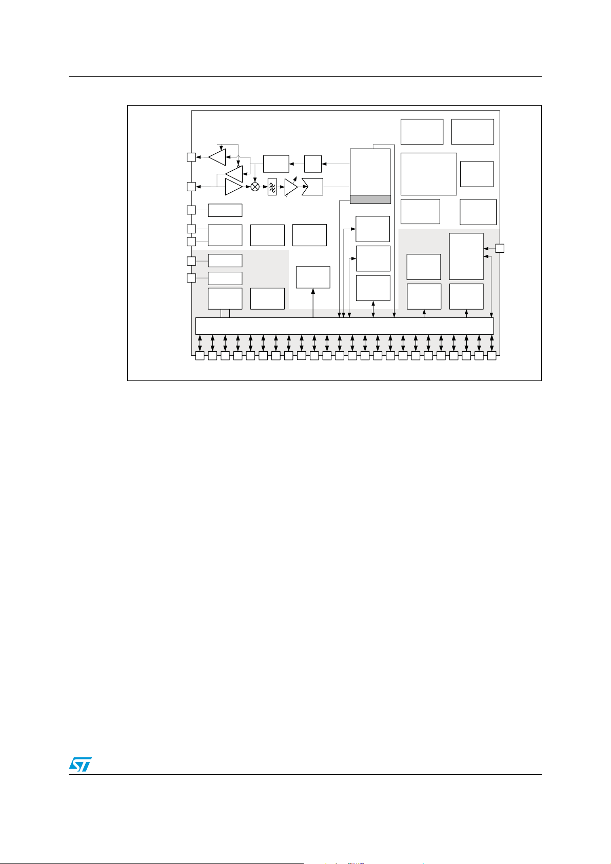
STM32W108CB, STM32W108HB Description
Packet sniffer
ADC
RF_P,N
Program
Flash
128 kBytes
Data
SRAM
8 kBytes
HF crystal
OSC
LF crystal
OSC
General
Purpose
ADC
Serial
Wire and
JTAG
debug
Internal LF
RC-OSC
GPIO multiplexor swtich
Chip
manage r
Regulator
Bias
2ndlevel
Interrupt
controller
RF_TX_ALT_P,N
OSCA
OSCB
PA[7:0], PB[7:0], PC[7:0]
Encryption
accl erator
IF
Always
Powered
Domain
ARM CORTEX-M3
®
CPU with NVIC
and MPU
VREG_OUT
Wat chdog
PA select
LNA
PA
PA
DAC
MAC
+
Baseband
Sleep
timer
BIAS_R
POR
nRESET
General
purpose
timers
GPIO
registers
UART/
SPI/TWI
SYNTH
Inte rnal H F
RC-OSC
TX_ACTIVE
SWCLK,
JTCK
Calibration
ADC
Packet Trace
CPU debug
TPIU/ITM/
FPB/DWT
Ai15250
Figure 1. STM32W block diagram
Doc ID 15851 Rev 1 3/20
Page 4
Electrical characteristics STM32W108CB, STM32W108HB
STM32W
C = 50 pF
STM32W
V
IN
2 Electrical characteristics
2.1 Parameter conditions
Unless otherwise specified, all voltages are referenced to VSS.
2.1.1 Minimum and maximum values
Unless otherwise specified the minimum and maximum values are guaranteed in the worst
conditions of ambient temperature, supply voltage and frequencies by tests in production on
100% of the devices with an ambient temperature at T
the selected temperature range).
Data based on characterization results, design simulation and/or technology characteristics
are indicated in the table footnotes and are not tested in production. Based on
characterization, the minimum and maximum values refer to sample tests and represent the
mean value plus or minus three times the standard deviation (mean ±3Σ).
2.1.2 Typical values
Unless otherwise specified, typical data are based on TA = 25 °C, VDD = 3.3 V (for the
2V≤ V
tested.
≤ 3.6 V voltage range). They are given only as design guidelines and are not
DD
= 25 °C and TA = TAmax (given by
A
Typical ADC accuracy values are determined by characterization of a batch of samples from
a standard diffusion lot over the full temperature range, where 95% of the devices have an
error less than or equal to the value indicated
2.1.3 Typical curves
Unless otherwise specified, all typical curves are given only as design guidelines and are
not tested.
2.1.4 Loading capacitor
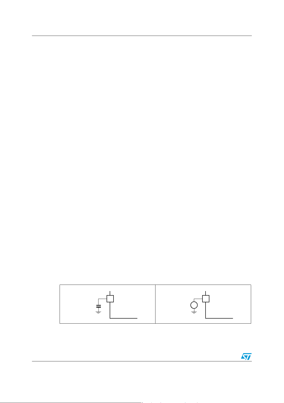
The loading conditions used for pin parameter measurement are shown in Figure 2.
2.1.5 Pin input voltage
The input voltage measurement on a pin of the device is described in Figure 3.
Figure 2. Pin loading conditions Figure 3. Pin input voltage
(mean ±2Σ).
4/20 Doc ID 15851 Rev 1
Page 5
STM32W108CB, STM32W108HB Electrical characteristics
2.2 Absolute maximum ratings
Stresses above the absolute maximum ratings listed in Table 2: Voltage characteristics,
Table 3: Current characteristics, and Table 4: Thermal characteristics may cause permanent
damage to the device. These are stress ratings only and functional operation of the device
at these conditions is not implied. Exposure to maximum rating conditions for extended
periods may affect device reliability.
Table 2. Voltage characteristics
Ratings Min. Max. Unit
Regulator input voltage (VDD_PADS) -0.3 +3.6 V
Analog, Memory and Core voltage (VDD_24MHZ, VDD_VCO,
VDD_RF, VDD_IF, VDD_PADSA, VDD_MEM, VDD_PRE,
VDD_SYNTH, VDD_CORE)
Voltage on RF_P,N; RF_TX_ALT_P,N -0.3 +3.6 V
-0.3 +2.0 V
RF Input Power (for max level for correct packet reception see
Table 11: Receive characteristics) RX signal into a lossless balun
Voltage on any GPIO (PA[7:0], PB[7:0], PC[7:0]), SWCLK, nRESET,
VREG_OUT
-0.3
Voltage on BIAS_R, OSCA, OSCB -0.3
Table 3. Current characteristics
+15 dBm
VDD_PADS
+0.3
VDD_PADSA
+0.3
Symbol Ratings Max. Unit
I
VDD
I
VSS
Total current into VDD/V
Total current out of V
power lines (source) 150
DDA
ground lines (sink) 150
SS
Output current sunk by any I/O and control pin 25
I
IO
Output current source by any I/Os and control pin − 25
Injected current on NRST pin ± 5
I
INJ(PIN)
Injected current on HSE OSC_IN and LSE OSC_IN pins ± 5
Injected current on any other pin ± 5
ΣI
INJ(PIN)
Table 4. Thermal characteristics
Total injected current (sum of all I/O and control pins) ± 25
Symbol Ratings Value Unit
V
V
mA
T
STG
T
J
Storage temperature range –40 to +140 °C
Maximum junction temperature 150 °C
Doc ID 15851 Rev 1 5/20
Page 6
Electrical characteristics STM32W108CB, STM32W108HB
2.3 Operating conditions
2.3.1 General operating conditions
Table 5. General operating conditions
Symbol Parameter Conditions Min. Typ. Max. Unit
– Regulator input voltage (VDD_PADS) 2.1 3.6 V
Analog and memory input voltage
(VDD_24MHZ, VDD_VCO, VDD_RF,
–
VDD_IF, VDD_PADSA, VDD_MEM,
VDD_PRE, VDD_SYNTH)
– Core input voltage (VDD_CORE) 1.18 1.25 1.32 V
– Operating temperature range -40 +85 °C
f
HCLK
PCLK1
f
PCLK2
V
Internal AHB clock frequency 0 72
Internal APB1 clock frequency 0 36
Internal APB2 clock frequency 0 72
Standard operating voltage 2 3.6 V
DD
Analog operating voltage
V
DDA
(ADC not used)
Analog operating voltage
Must be the same
potential as V
DD
(ADC used)
1.7 1.8 1.9 V
MHzf
23.6
V
2.4 3.6
V
Backup operating voltage 1.8 3.6 V
BAT
Maximum power
Ambient temperature for 6 suffix
version
dissipation
Low power
dissipation
TA
Maximum power
Ambient temperature for 7 suffix
version
dissipation
Low power
dissipation
6 suffix version –40 105
J Junction temperature range
T
7 suffix version –40 125
2.3.2 Absolute maximum ratings (electrical sensitivity)
Based on three different tests (ESD, LU) using specific measurement methods, the device is
stressed in order to determine its performance in terms of electrical sensitivity.
Electrostatic discharge (ESD)
Electrostatic discharges (a positive then a negative pulse separated by 1 second) are
applied to the pins of each sample according to each pin combination. The sample size
depends on the number of supply pins in the device (3 parts × (n+1) supply pins). This test
conforms to the JESD22-A114/C101 standard.
–40 85
°C
–40 105
–40 105
°C
–40 125
°C
6/20 Doc ID 15851 Rev 1
Page 7

STM32W108CB, STM32W108HB Electrical characteristics
Table 6. ESD absolute maximum ratings
Symbol Ratings Conditions Class Maximum value
(1)
Unit
TA = +25 °C
conforming to
JESD22-A114
2 ±2000
V
ESD(HBM)
Electrostatic discharge
voltage (human body model)
Electrostatic discharge
V
ESD(CDM)
voltage (charge device
model) for non-RF pins
Electrostatic discharge
voltage (charge device
TA = +25 °C
conforming to
JESD22-C101
II
±400
±225
model)for RF pins
MSL Moisture sensitivity level MSL3 –
1. Based on characterization results, not tested in production.
Static latch-up
Two complementary static tests are required on six parts to assess the latch-up
performance:
● A supply overvoltage is applied to each power supply pin
● A current injection is applied to each input, output and configurable I/O pin
These tests are compliant with EIA/JESD 78A IC latch-up standard.
Table 7. Electrical sensitivities
Symbol Parameter Conditions Class
V
LU Static latch-up class T
= +105 °C conforming to JESD78A II level A
A
2.4 DC electrical characteristics
Table 8. DC electrical characteristics
Parameter Conditions Min. Typ. Max. Unit
Regulator input voltage
(VDD_PADS)
Power supply range (VDD_MEM)
Power supply range
(VDD_CORE)
Deep Sleep Current
Quiescent current, internal RC
oscillator disabled
Regulator output or external
input
Regulator output 1.18 1.25 1.32 V
-40°C, VDD_PADS = 3.6 V 0.4 µA
+25°C, VDD_PADS = 3.6 V 0.4 µA
+85°C, VDD_PADS = 3.6 V 0.6 µA
2.1 3.6 V
1.7 1.8 1.9 V
Doc ID 15851 Rev 1 7/20
Page 8

Electrical characteristics STM32W108CB, STM32W108HB
Table 8. DC electrical characteristics (continued)
Parameter Conditions Min. Typ. Max. Unit
-40°C, VDD_PADS=3.6 V 0.7 µA
Quiescent current, including
internal RC oscillator
Quiescent current, including
32.768 kHz oscillator
+25°C, VDD_PADS=3.6 V 0.8 µA
+85°C, VDD_PADS=3.6 V 1.2 µA
-40°C, VDD_PADS=3.6V 1.2 µA
+25°C, VDD_PADS=3.6 V 1.3 µA
+85°C, VDD_PADS=3.6 V 1.7 µA
Quiescent current, including
internal RC oscillator and 32.768
kHz oscillator
Simulated deep sleep (debug
mode) current
Reset current
Quiescent current, nRESET
asserted
Processor and peripheral currents
®
ARM
Cortex-M3, RAM, and flash
memory
®
ARM
Cortex-M3, RAM, and flash
memory
®
ARM
Cortex-M3, RAM, and flash
memory sleep current
®
ARM
Cortex-M3, RAM, and flash
memory sleep current
-40°C, VDD_PADS=3.6V 1.4 µA
+25°C, VDD_PADS=3.6V 1.5 µA
+85°C, VDD_PADS=3.6 V 2.0 µA
With no debugger activity 200 µA
Typ at 25°C/3 V
Max at 85°C/3.6 V
1.2 mA
25°C, 1.8 V memory and 1.25
V core
ARM® Cortex-M3 running at 12
8.0 mA
MHz from crystal oscillator
Radio and all peripherals off
25°C, 1.8 V memory and 1.25
V core
®
Cortex-M3 running at 24
ARM
9.0 mA
MHz from crystal oscillator
Radio and all peripherals off
25°C, 1.8 V memory and 1.25
V core
®
ARM
Cortex-M3 clocked at 12
4.0 mA
MHz from the crystal oscillator
Radio and all peripherals off
25°C, 1.8 V memory and 1.25
V core
®
Cortex-M3 clocked at 6
ARM
MHz from the high frequency
2.0 mA
RC oscillator
Radio and all peripherals off
Serial controller current
General purpose timer current
For each controller at
maximum data rate
For each timer at maximum
clock rate
8/20 Doc ID 15851 Rev 1
0.2 mA
0.1 mA
Page 9

STM32W108CB, STM32W108HB Electrical characteristics
Table 8. DC electrical characteristics (continued)
Parameter Conditions Min. Typ. Max. Unit
General purpose ADC current
Rx current
Radio receiver, MAC, and
baseband
Total RX current ( = I
MAC and baseband, CPU
Flash memory )
Radio receiver,
+ I
RAM, and
Boost mode total RX current ( =
I
Radio receiver, MAC and baseband,
+ I
RAM, and Flash memory )
CPU
Tx current
Radio transmitter, MAC, and
baseband
At maximum sample rate, DMA
enabled
®
Cortex-M3 sleeping 20.0 mA
ARM
VDD_PADS = 3.0 V, 25°C,
®
ARM
Cortex-M3 running at 12
1.1 mA
27.0 mA
MHz
VDD_PADS = 3.0 V, 25°C,
®
ARM
Cortex-M3 running at 24
28.0 mA
MHz
VDD_PADS = 3.0 V, 25°C,
®
ARM
Cortex-M3 running at 12
28.0 mA
MHz
VDD_PADS = 3.0 V, 25°C,
®
ARM
Cortex-M3 running at 24
29.0 mA
MHz
25°C and 1.8 V core; max.
power out (+3 dBm typical)
®
ARM
Cortex-M3 sleeping
26.0 mA
VDD_PADS = 3.0 V, 25°C;
maximum power setting
(+7dBm); ARM
®
Cortex-M3
40.0 mA
running at 24 MHz
Total Tx current ( = I
MAC and baseband, CPU
Flash memory )
Radio transmitter,
+ I
RAM, and
VDD_PADS = 3.0 V, 25°C;
+3dBm power setting; ARM
®
32.0 mA
Cortex-M3 running at 24 MHz
VDD_PADS = 3.0 V, 25°C;
0dBm power setting; ARM
®
29.5 mA
Cortex-M3 running at 24 MHz
VDD_PADS = 3.0 V, 25°C;
minimum power setting; ARM
®
24.5 mA
Cortex-M3 running at 24 MHz
Doc ID 15851 Rev 1 9/20
Page 10

Electrical characteristics STM32W108CB, STM32W108HB
Figure 4 shows the variation of current in transmit mode (with the ARM® Cortex-M3 running
at 24 MHz).
Figure 4. Transmit power consumption
Figure 5 shows typical output power against power setting on the ST reference design.
Figure 5. Transmit output power
10/20 Doc ID 15851 Rev 1
Page 11

STM32W108CB, STM32W108HB Electrical characteristics
2.5 Digital I/O specifications
Ta bl e 9 lists the digital I/O specifications for the STM32W. The digital I/O power (named
VDD_PADS) comes from three dedicated pins (Pins 23, 28 and 37). The voltage applied to
these pins sets the I/O voltage.
Table 9. Digital I/O specifications
Parameter Conditions Min. Typ. Max. Unit
Voltage supply (Regulator Input) VDD_PADS 2.1 3.6 V
V
Low Schmitt switching threshold
High Schmitt switching
threshold
SWIL
Schmitt input threshold
going from high to low
V
SWIH
Schmitt input threshold
going from low to high
0.42 x
VDD_PADS
0.62 x
VDD_PADS
0.50 x
VDD_PADS
0.80 x
VDD_PADS
V
V
Input current for logic 0 I
Input current for logic 1 I
Input pull-up resistor value R
Input pull-down resistor value R
Output voltage for logic 0
Output voltage for logic 1
Output source current (standard
current pad)
Output sink current (standard
current pad)
Output source current
high current pad: PA6, PA7,
PB6, PB7, PC0
Output sink current
high current pad: PA6, PA7,
PB6, PB7, PC0
IL
IH
IPU
IPD
V
OL
(IOL = 4 mA for standard
pads, 8 mA for high current
pads)
V
OH
(IOH = 4 mA for standard
pads, 8 mA for high current
pads)
I
OHS
I
OLS
I
OHH
I
OLH
-0.5 µAA
+0.5 µAA
24 29 34 kΩ
24 29 34 kΩ
0
0.82 x
VDD_PADS
0.18 x
VDD_PADS
VDD_PADS V
4mA
4mA
8mA
8mA
V
Total output current (for I/O
Pads)
Input voltage threshold for
OSC32A
Input voltage threshold for
OSCA
I
OH
+ I
OL
0.2 x
VDD_PADS
0.2 x
VDD_PADS
40 mA
0.8 x
VDD_PADS
0.8 x
VDD_PADSAV
V
A
Doc ID 15851 Rev 1 11/20
Page 12

Electrical characteristics STM32W108CB, STM32W108HB
2.6 Non-RF system electrical characteristics
Ta bl e 1 0 lists the non-RF system level characteristics for the STM32W.
Table 10. Non-RF system electrical characteristics
Parameter Conditions Min. Typ. Max. Unit
From wakeup event to first ARM® Cortex-
System wake time
from deep sleep
M3 instruction running from 6MHz internal
RC clock
Includes supply ramp time and oscillator
startup time
–100– µs
Shutdown time going
into deep sleep
From last ARM® Cortex-M3 instruction to
deep sleep mode
–5–µs
2.7 RF electrical characteristics
2.7.1 Receive
Ta bl e 1 1 lists the key parameters of the integrated IEEE 802.15.4 receiver on the STM32W.
Note: Receive measurements were collected with ST’s STM32W Ceramic Balun Reference
Design (Version A0) at 2440 MHz. The Typical number indicates one standard deviation
above the mean, measured at room temperature (25
measured over process corners at room temperature
Table 11. Receive characteristics
Parameter Conditions Min. Typ. Max. Unit
Frequency range 2400 2500 MHz
Sensitivity (boost mode)
Sensitivity
High-side adjacent channel
rejection
1% PER, 20 byte packet
defined by IEEE 802.15.4-2003
1% PER, 20 byte packet
defined by IEEE 802.15.4-2003
IEEE 802.15.4 signal at -82
dBm
°
C). The Min and Max numbers were
-100 -95 dBm
-99 -94 dBm
35 dB
Low-side adjacent channel
rejection
nd
high-side adjacent channel
2
rejection
nd
low-side adjacent channel
2
rejection
Channel rejection for all other
channels
802.11g rejection centered at +12
MHz or -13 MHz
Maximum input signal level for
correct operation
12/20 Doc ID 15851 Rev 1
IEEE 802.15.4 signal at -82
dBm
IEEE 802.15.4 signal at -82
dBm
IEEE 802.15.4 signal at -82
dBm
IEEE 802.15.4 signal at -82
dBm
IEEE 802.15.4 signal at -82
dBm
35 dB
43 dB
43 dB
40 dB
35 dB
0dBm
Page 13

STM32W108CB, STM32W108HB Electrical characteristics
Table 11. Receive characteristics (continued)
Parameter Conditions Min. Typ. Max. Unit
Co-channel rejection
Relative frequency error
(2x40 ppm required by IEEE
802.15.4)
Relative timing error
(2x40 ppm required by IEEE
802.15.4)
Linear RSSI range As defined by IEEE 802.15.4 40 dB
RSSI Range -90 -30 dBm
IEEE 802.15.4 signal at -82
dBm
-6 dBc
-120 +120 ppm
-120 +120 ppm
2.7.2 Transmit
Ta bl e 1 2 lists the key parameters of the integrated IEEE 802.15.4 transmitter on the
STM32W.
Note: Transmit measurements were collected with ST’s STM32W Ceramic Balun Reference
Design (Version A0) at 2440 MHz. The Typical number indicates one standard deviation
above the mean, measured at room temperature (25
measured over process corners at room temperature
Table 12. Transmit characteristics
Parameter Conditions Min. Typ. Max. Unit
°
C). The Min and Max numbers were
Maximum output power (boost
mode)
Maximum output power At highest power setting 0 3 dBm
Minimum output power At lowest power setting -32 dBm
Error vector magnitude
Carrier frequency error -40 +40 ppm
Load impedance for optimum
transmit power
PSD mask relative 3.5 MHz away -20 dB
PSD mask absolute 3.5 MHz away -30 dBm
At highest power setting 7 dBm
As defined by IEEE 802.15.4,
which sets a 35% maximum
515%
200+j90
TBC
?
Doc ID 15851 Rev 1 13/20
Page 14

Electrical characteristics STM32W108CB, STM32W108HB
2.7.3 Synthesizer
Ta bl e 1 3 lists the key parameters of the integrated synthesizer on the STM32W.
Table 13. Synthesizer characteristics
Parameter Conditions Min. Typ. Max. Unit
Frequency range 2400 2500 MHz
Frequency resolution 11.7 kHz
Lock time
Relock time
Phase noise at 100 kHz offset -71 dBc/Hz
Phase noise at 1 MHz offset -91 dBc/Hz
Phase noise at 4 MHz offset -103 dBc/Hz
Phase noise at 10 MHz offset -111 dBc/Hz
From off, with correct VCO DAC
setting
Channel change or RX/TX
turnaround (IEEE 802.15.4
defines 192 µs turnaround s turnaround
time)
100 µss
100 µss
14/20 Doc ID 15851 Rev 1
Page 15

STM32W108CB, STM32W108HB Package characteristics
Seating
Plane
C
A3
A1
A2
A
ddd C
Pin no. 1 ID
R = 0.20
Bottom View
1
48
e
E
L
L
12
13
D2
b
24
25
b
E2
36
37
e
D
V0_ME
3 Package characteristics
3.1 Package mechanical data
In order to meet environmental requirements, ST offers these devices in different grades of
ECOPACK
®
packages, depending on their level of environmental compliance. ECOPACK®
specifications, grade definitions and product status are available at: www.st.com.
ECOPACK
®
is an ST trademark.
Figure 6. VFQFPN48 7x7mm package outline
Doc ID 15851 Rev 1 15/20
Page 16

Package characteristics STM32W108CB, STM32W108HB
Table 14. VFQFPN48 7x7mm package mechanical data
Millimeters Inches
Symbol
Min. Typ. Max. Min. Typ. Max.
A 0.800 0.900 1.000 0.0315 0.0354 0.0394
A1 0.020 0.050 0.0008 0.0020
A2 0.650 1.000 0.0256 0.0394
A3 0.250 0.0098
b 0.180 0.230 0.300 0.0071 0.0091 0.0118
D 6.850 7.000 7.150 0.2697 0.2756 0.2815
D2 2.250 4.700 5.250 0.0886 0.1850 0.2067
E 6.850 7.000 7.150 0.2697 0.2756 0.2815
E2 2.250 4.700 5.250 0.0886 0.1850 0.2067
e 0.450 0.500 0.550 0.0177 0.0197 0.0217
L 0.300 0.400 0.500 0.0118 0.0157 0.0197
ddd 0.080 0.0031
(1)
1. Values in inches are converted from mm and rounded to 4 decimal digits.
16/20 Doc ID 15851 Rev 1
Page 17

STM32W108CB, STM32W108HB Package characteristics
Bottom view
Exposed pad
Top view
Pin 1 ID
Pin 1 ID
ZF_ME
Figure 7. QFN 40L 6x6mm pitch 0.5 package outline
Table 15. QFN 40L 6x6mm package mechanical data
millimeters inches
(1)
Symbol
Min Typ Max Min Typ Max
A 0.800 0.900 1.000 0.0315 0.0354 0.0394
A1 0.020 0.050 0.0008 0.0020
A2 0.720 1.070 0.0283 0.0421
A3 0.200 0.0079
b 0.180 0.250 0.300 0.0071 0.0098 0.0118
D 5.900 6.000 6.100 0.2323 0.2362 0.2402
D2 4.500 4.550 4.700 0.1772 0.1791 0.1850
E 6.000 0.2362
E2 4.500 4.550 4.700 0.1772 0.1791 0.1850
e 0.500 0.0197
L 0.350 0.400 0.450 0.0138 0.0157 0.0177
ddd 0.080 0.0031
1. Values in inches are converted from mm and rounded to 4 decimal digits.
Doc ID 15851 Rev 1 17/20
Page 18

Ordering information scheme STM32W108CB, STM32W108HB
4 Ordering information scheme
Example: STM32 W 108 C B U 6 x
Device family
STM32 = ARM-based 32-bit microcontroller
Product type
W = wireless system-on-chip
Sub-family
108 = IEEE 802.15.4 specification
Pin count
H = 40 pins
C = 48 pins
Code size
B = 128 Kbytes
Package
U = QFN
Temperature range
6 = –40 °C to +85 °C
Firmware version
“Blank” = Open platform
1 = Ember ZigBee stack
2 = ST ZigBee stack
3 = RF4CE stack
4 = IEEE 802.15.4 media access control
For a list of available options (speed, package, etc.) or for further information on any aspect
of this device, please contact your nearest ST sales office.
18/20 Doc ID 15851 Rev 1
Page 19

STM32W108CB, STM32W108HB Revision history
5 Revision history
Table 16. Document revision history
Date Revision Changes
20-Aug-2009 1 Initial release.
Doc ID 15851 Rev 1 19/20
Page 20

STM32W108CB, STM32W108HB
Please Read Carefully:
Information in this document is provided solely in connection with ST products. STMicroelectronics NV and its subsidiaries (“ST”) reserve the
right to make changes, corrections, modifications or improvements, to this document, and the products and services described herein at any
time, without notice.
All ST products are sold pursuant to ST’s terms and conditions of sale.
Purchasers are solely responsible for the choice, selection and use of the ST products and services described herein, and ST assumes no
liability whatsoever relating to the choice, selection or use of the ST products and services described herein.
No license, express or implied, by estoppel or otherwise, to any intellectual property rights is granted under this document. If any part of this
document refers to any third party products or services it shall not be deemed a license grant by ST for the use of such third party products
or services, or any intellectual property contained therein or considered as a warranty covering the use in any manner whatsoever of such
third party products or services or any intellectual property contained therein.
UNLESS OTHERWISE SET FORTH IN ST’S TERMS AND CONDITIONS OF SALE ST DISCLAIMS ANY EXPRESS OR IMPLIED
WARRANTY WITH RESPECT TO THE USE AND/OR SALE OF ST PRODUCTS INCLUDING WITHOUT LIMITATION IMPLIED
WARRANTIES OF MERCHANTABILITY, FITNESS FOR A PARTICULAR PURPOSE (AND THEIR EQUIVALENTS UNDER THE LAWS
OF ANY JURISDICTION), OR INFRINGEMENT OF ANY PATENT, COPYRIGHT OR OTHER INTELLECTUAL PROPERTY RIGHT.
UNLESS EXPRESSLY APPROVED IN WRITING BY AN AUTHORIZED ST REPRESENTATIVE, ST PRODUCTS ARE NOT
RECOMMENDED, AUTHORIZED OR WARRANTED FOR USE IN MILITARY, AIR CRAFT, SPACE, LIFE SAVING, OR LIFE SUSTAINING
APPLICATIONS, NOR IN PRODUCTS OR SYSTEMS WHERE FAILURE OR MALFUNCTION MAY RESULT IN PERSONAL INJURY,
DEATH, OR SEVERE PROPERTY OR ENVIRONMENTAL DAMAGE. ST PRODUCTS WHICH ARE NOT SPECIFIED AS "AUTOMOTIVE
GRADE" MAY ONLY BE USED IN AUTOMOTIVE APPLICATIONS AT USER’S OWN RISK.
Resale of ST products with provisions different from the statements and/or technical features set forth in this document shall immediately void
any warranty granted by ST for the ST product or service described herein and shall not create or extend in any manner whatsoever, any
liability of ST.
ST and the ST logo are trademarks or registered trademarks of ST in various countries.
Information in this document supersedes and replaces all information previously supplied.
The ST logo is a registered trademark of STMicroelectronics. All other names are the property of their respective owners.
© 2009 STMicroelectronics - All rights reserved
STMicroelectronics group of companies
Australia - Belgium - Brazil - Canada - China - Czech Republic - Finland - France - Germany - Hong Kong - India - Israel - Italy - Japan -
Malaysia - Malta - Morocco - Philippines - Singapore - Spain - Sweden - Switzerland - United Kingdom - United States of America
www.st.com
20/20 Doc ID 15851 Rev 1
 Loading...