

www.DataSheet4U.com
查询STM32F101x6供应商查询STM32F101x6供应商
STM32F101x6
STM32F101x8 STM32F101xB
Access line, advanced ARM-based 32-bit MCU with Flash memory,
six 16-bit timers, ADC and seven communication interfaces
Preliminary Data
Features
■ Core: ARM 32-bit Cortex™-M3
– 36 MHz, 45 DMIPS with 1.25 DMIPS/MHz
– Single-cycle multiplication and hardware
division
– Nested interrupt controller with 43
maskable interrupt channels
– Interrupt processing (down to 6 CPU
cycles) with tail chaining
■ Memories
– 32-to -1 2 8 Kbytes of Flash me m ory
– 6-to- 16 Kbytes of SRAM
■ Clock, reset and supply management
– 2.0 to 3.6 V application supply and I/Os
– POR, PDR and programmable voltage
detector (PVD)
– 4-to-16 MHz high-speed quartz oscillator
– Internal 8 MHz factory-trimmed RC
– Internal 32 kHz RC
– PLL for CPU clock
– Dedicated 32 kHz oscillator for RTC with
calibration
■ Low power
– Sleep, Stop and Standby modes
–V
■ Debug mode
supply for RTC and backup registers
BAT
– Serial wire debug (SWD) and JTAG
interfaces
■ DMA
– 7-channel DMA controller
– Peripherals supported: timers, ADC, SPIs,
2
I
Cs and USARTs
■ 12-bit, 1 µs A/D converter (16-channel)
– Conversion range: 0 to 3.6 V
CPU
LQFP48
7 x 7 mm
LQFP64
10 x 10 mm
LQFP100
14 x 14 mm
– Temperature sensor
■ Up to 80 fast I/O ports
– 32/49/80 5 V-tolerant I/Os
– All mappable on 16 external interrupt
vectors
– Atomi c re ad /m o dif y/write operations
■ Up to 6 timers
– Up to three 16-bit timers, each with up to 4
IC/OC/PWM or pulse counter
– 2 x 16-bit watchdog timers (Independent
and Window)
– SysTick timer: 24-bit downcounter
■ Up to 7 communication interfaces
– Up to 2 x I
2
C interfaces (SMBus/PMBus)
– Up to 3 USARTs (ISO 7816 interface, LIN,
IrDA capability, modem control)
– Up to 2 SPIs (18 Mbit/s)
Table 1. Device summary
Reference Root part number
STM32F101x6 STM32F101C6, STM32F101R6
STM32F101x8
STM32F101xB STM32F101RB, STM32F101VB
STM32F101C8, STM32F101R8
STM32F101V8
July 2007 Rev 2 1/64
This is preliminary information on a new product now in development or undergoing ev aluation. Details are subject to
change without notice.
www.st.com
1

Contents STM32F101xx
Contents
1 Introduction . . . . . . . . . . . . . . . . . . . . . . . . . . . . . . . . . . . . . . . . . . . . . . . . 6
2 Description . . . . . . . . . . . . . . . . . . . . . . . . . . . . . . . . . . . . . . . . . . . . . . . . . 6
2.1 Device overview . . . . . . . . . . . . . . . . . . . . . . . . . . . . . . . . . . . . . . . . . . . . . 7
2.2 Overview . . . . . . . . . . . . . . . . . . . . . . . . . . . . . . . . . . . . . . . . . . . . . . . . . . 8
3 Pin descriptions . . . . . . . . . . . . . . . . . . . . . . . . . . . . . . . . . . . . . . . . . . . 14
4 Memory mapping . . . . . . . . . . . . . . . . . . . . . . . . . . . . . . . . . . . . . . . . . . 20
5 Electrical characteristics . . . . . . . . . . . . . . . . . . . . . . . . . . . . . . . . . . . . 21
5.1 Test conditions . . . . . . . . . . . . . . . . . . . . . . . . . . . . . . . . . . . . . . . . . . . . . 21
5.1.1 Minimum and maximum values . . . . . . . . . . . . . . . . . . . . . . . . . . . . . . . 21
5.1.2 Typical values . . . . . . . . . . . . . . . . . . . . . . . . . . . . . . . . . . . . . . . . . . . . . 21
5.1.3 Typical curves . . . . . . . . . . . . . . . . . . . . . . . . . . . . . . . . . . . . . . . . . . . . 21
5.1.4 Loading capacitor . . . . . . . . . . . . . . . . . . . . . . . . . . . . . . . . . . . . . . . . . 21
5.1.5 Pin input voltage . . . . . . . . . . . . . . . . . . . . . . . . . . . . . . . . . . . . . . . . . . 21
5.1.6 Power supply scheme . . . . . . . . . . . . . . . . . . . . . . . . . . . . . . . . . . . . . . 22
5.1.7 Current consumption measurement . . . . . . . . . . . . . . . . . . . . . . . . . . . 23
5.2 Absolute maximum ratings . . . . . . . . . . . . . . . . . . . . . . . . . . . . . . . . . . . . 24
5.3 Operating conditions . . . . . . . . . . . . . . . . . . . . . . . . . . . . . . . . . . . . . . . . 26
5.3.1 General operating conditions . . . . . . . . . . . . . . . . . . . . . . . . . . . . . . . . . 26
5.3.2 Operating conditions at power-up / power-down . . . . . . . . . . . . . . . . . . 26
5.3.3 Embedded reset and power control block characteristics . . . . . . . . . . . 27
5.3.4 Embedded reference voltage . . . . . . . . . . . . . . . . . . . . . . . . . . . . . . . . . 27
5.3.5 Supply current characteristics . . . . . . . . . . . . . . . . . . . . . . . . . . . . . . . . 28
5.3.6 External clock source characteristics . . . . . . . . . . . . . . . . . . . . . . . . . . . 32
5.3.7 Internal Clock source characteristics . . . . . . . . . . . . . . . . . . . . . . . . . . . 36
5.3.8 PLL characteristics . . . . . . . . . . . . . . . . . . . . . . . . . . . . . . . . . . . . . . . . 37
5.3.9 Memory characteristics . . . . . . . . . . . . . . . . . . . . . . . . . . . . . . . . . . . . . 38
5.3.10 EMC characteristics . . . . . . . . . . . . . . . . . . . . . . . . . . . . . . . . . . . . . . . . 39
5.3.11 Absolute maximum ratings (electrical sensitivity) . . . . . . . . . . . . . . . . . 40
5.3.12 I/O port characteristics . . . . . . . . . . . . . . . . . . . . . . . . . . . . . . . . . . . . . . 42
5.3.13 NRST pin characteristics . . . . . . . . . . . . . . . . . . . . . . . . . . . . . . . . . . . . 47
2/64

STM32F101xx Contents
5.3.14 TIM timer characteristics . . . . . . . . . . . . . . . . . . . . . . . . . . . . . . . . . . . . 48
5.3.15 Communications interfaces . . . . . . . . . . . . . . . . . . . . . . . . . . . . . . . . . . 49
5.3.16 12-bit ADC characteristics . . . . . . . . . . . . . . . . . . . . . . . . . . . . . . . . . . . 54
5.3.17 Temperature sensor characteristics . . . . . . . . . . . . . . . . . . . . . . . . . . . . 57
6 Package characteristics . . . . . . . . . . . . . . . . . . . . . . . . . . . . . . . . . . . . . 58
6.1 Thermal characteristics . . . . . . . . . . . . . . . . . . . . . . . . . . . . . . . . . . . . . . 61
7 Order codes . . . . . . . . . . . . . . . . . . . . . . . . . . . . . . . . . . . . . . . . . . . . . . . 62
7.1 Future family enhancements . . . . . . . . . . . . . . . . . . . . . . . . . . . . . . . . . . 62
8 Revision history . . . . . . . . . . . . . . . . . . . . . . . . . . . . . . . . . . . . . . . . . . . 63
3/64

List of tables STM32F101xx
List of tables
Table 1. Device summary. . . . . . . . . . . . . . . . . . . . . . . . . . . . . . . . . . . . . . . . . . . . . . . . . . . . . . . . . . 1
Table 2. Device features and peripheral counts (STM32F101xx access line) . . . . . . . . . . . . . . . . . . 7
Table 3. Pin definitions . . . . . . . . . . . . . . . . . . . . . . . . . . . . . . . . . . . . . . . . . . . . . . . . . . . . . . . . . . . 16
Table 4. Voltage characteristics . . . . . . . . . . . . . . . . . . . . . . . . . . . . . . . . . . . . . . . . . . . . . . . . . . . . 24
Table 5. Current characteristics . . . . . . . . . . . . . . . . . . . . . . . . . . . . . . . . . . . . . . . . . . . . . . . . . . . . 24
Table 6. Thermal characteristics. . . . . . . . . . . . . . . . . . . . . . . . . . . . . . . . . . . . . . . . . . . . . . . . . . . . 25
Table 7. General operating conditions . . . . . . . . . . . . . . . . . . . . . . . . . . . . . . . . . . . . . . . . . . . . . . . 26
Table 8. Operating conditions at power-up / power-down . . . . . . . . . . . . . . . . . . . . . . . . . . . . . . . . 26
Table 9. Embedded reset and power control block characteristics. . . . . . . . . . . . . . . . . . . . . . . . . . 27
Table 10. Embedded internal reference voltage. . . . . . . . . . . . . . . . . . . . . . . . . . . . . . . . . . . . . . . . . 27
Table 11. Maximum current consumption in Run and Sleep modes (T
Table 12. Maximum current consumption in Stop and Standby modes . . . . . . . . . . . . . . . . . . . . . . . 29
Table 13. Typical current consumption in Run and Sleep modes . . . . . . . . . . . . . . . . . . . . . . . . . . . 30
Table 14. Typical current consumption in Stop and Standby modes . . . . . . . . . . . . . . . . . . . . . . . . . 31
Table 15. High-speed user external (HSE) clock characteristics . . . . . . . . . . . . . . . . . . . . . . . . . . . . 32
Table 16. Low-speed user external clock characteristics . . . . . . . . . . . . . . . . . . . . . . . . . . . . . . . . . . 32
Table 17. HSE 4-16 MHz oscillator characteristics. . . . . . . . . . . . . . . . . . . . . . . . . . . . . . . . . . . . . . . 34
Table 18. LSE oscillator characteristics (
= 32.768 kHz) . . . . . . . . . . . . . . . . . . . . . . . . . . . . . . . 35
fLSE
Table 19. HSI oscillator characteristics. . . . . . . . . . . . . . . . . . . . . . . . . . . . . . . . . . . . . . . . . . . . . . . . 36
Table 20. LSI oscillator characteristics . . . . . . . . . . . . . . . . . . . . . . . . . . . . . . . . . . . . . . . . . . . . . . . 36
Table 21. Low-power mode wakeup timings . . . . . . . . . . . . . . . . . . . . . . . . . . . . . . . . . . . . . . . . . . . 37
Table 22. PLL characteristics . . . . . . . . . . . . . . . . . . . . . . . . . . . . . . . . . . . . . . . . . . . . . . . . . . . . . . . 37
Table 23. Flash memory characteristics. . . . . . . . . . . . . . . . . . . . . . . . . . . . . . . . . . . . . . . . . . . . . . . 38
Table 24. Flash endurance and data retention. . . . . . . . . . . . . . . . . . . . . . . . . . . . . . . . . . . . . . . . . . 38
Table 25. EMS characteristics . . . . . . . . . . . . . . . . . . . . . . . . . . . . . . . . . . . . . . . . . . . . . . . . . . . . . . 39
Table 26. EMI characteristics . . . . . . . . . . . . . . . . . . . . . . . . . . . . . . . . . . . . . . . . . . . . . . . . . . . . . . . 40
Table 27. ESD absolute maximum ratings . . . . . . . . . . . . . . . . . . . . . . . . . . . . . . . . . . . . . . . . . . . . . 40
Table 28. Electrical sensitivities . . . . . . . . . . . . . . . . . . . . . . . . . . . . . . . . . . . . . . . . . . . . . . . . . . . . . 41
Table 29. I/O static characteristics . . . . . . . . . . . . . . . . . . . . . . . . . . . . . . . . . . . . . . . . . . . . . . . . . . . 42
Table 30. Output voltage characteristics . . . . . . . . . . . . . . . . . . . . . . . . . . . . . . . . . . . . . . . . . . . . . . 44
Table 31. I/O AC characteristics. . . . . . . . . . . . . . . . . . . . . . . . . . . . . . . . . . . . . . . . . . . . . . . . . . . . . 45
Table 32. NRST pin characteristics . . . . . . . . . . . . . . . . . . . . . . . . . . . . . . . . . . . . . . . . . . . . . . . . . . 47
Table 33. TIMx characteristics . . . . . . . . . . . . . . . . . . . . . . . . . . . . . . . . . . . . . . . . . . . . . . . . . . . . . . 48
Table 34. I
Table 35. SCL frequency (f
2
C characteristics. . . . . . . . . . . . . . . . . . . . . . . . . . . . . . . . . . . . . . . . . . . . . . . . . . . . . . . . 49
= 36 MHz, VDD = 3.3 V) . . . . . . . . . . . . . . . . . . . . . . . . . . . . . . . . . 50
PCLK1
Table 36. SPI characteristics . . . . . . . . . . . . . . . . . . . . . . . . . . . . . . . . . . . . . . . . . . . . . . . . . . . . . . . 51
Table 37. ADC characteristics . . . . . . . . . . . . . . . . . . . . . . . . . . . . . . . . . . . . . . . . . . . . . . . . . . . . . . 54
Table 38. ADC accuracy (f
PCLK2
= 10 MHz, f
= 10 MHz, R
ADC
AIN
Table 39. TS characteristics . . . . . . . . . . . . . . . . . . . . . . . . . . . . . . . . . . . . . . . . . . . . . . . . . . . . . . . . 57
Table 40. LQPF100 – 100-pin low-profile quad flat package mechanical data . . . . . . . . . . . . . . . . . 58
Table 41. LQFP64 – 64-pin low-profile quad flat package mechanical data . . . . . . . . . . . . . . . . . . . 59
Table 42. LQFP48 – 48-pin low-profile quad flat package mechanical data . . . . . . . . . . . . . . . . . . . 60
Table 43. Thermal characteristics. . . . . . . . . . . . . . . . . . . . . . . . . . . . . . . . . . . . . . . . . . . . . . . . . . . . 61
Table 44. Order codes . . . . . . . . . . . . . . . . . . . . . . . . . . . . . . . . . . . . . . . . . . . . . . . . . . . . . . . . . . . . 62
Table 45. Document revision history . . . . . . . . . . . . . . . . . . . . . . . . . . . . . . . . . . . . . . . . . . . . . . . . . 63
= 85 °C) . . . . . . . . . . . . . . . 28
A
< 10 kΩ, V
= 3.3 V) . . . . . . . . 55
DDA
4/64

STM32F101xx List of figures
List of figures
Figure 1. STM32F101xx access line block diagram . . . . . . . . . . . . . . . . . . . . . . . . . . . . . . . . . . . 13
Figure 2. STM32F101xx access line LQFP100 pinout . . . . . . . . . . . . . . . . . . . . . . . . . . . . . . . . . . . 14
Figure 3. STM32F101xx access line LQFP64 pinout . . . . . . . . . . . . . . . . . . . . . . . . . . . . . . . . . . . . 15
Figure 4. STM32F101xx access line LQFP48 pinout . . . . . . . . . . . . . . . . . . . . . . . . . . . . . . . . . . . . 15
Figure 5. Memory map. . . . . . . . . . . . . . . . . . . . . . . . . . . . . . . . . . . . . . . . . . . . . . . . . . . . . . . . . . . . 20
Figure 6. Pin loading conditions. . . . . . . . . . . . . . . . . . . . . . . . . . . . . . . . . . . . . . . . . . . . . . . . . . . . . 22
Figure 7. Pin input voltage . . . . . . . . . . . . . . . . . . . . . . . . . . . . . . . . . . . . . . . . . . . . . . . . . . . . . . . . . 22
Figure 8. Power supply scheme. . . . . . . . . . . . . . . . . . . . . . . . . . . . . . . . . . . . . . . . . . . . . . . . . . . . . 22
Figure 9. Current consumption measurement scheme . . . . . . . . . . . . . . . . . . . . . . . . . . . . . . . . . . . 23
Figure 10. High-speed external clock source AC timing diagram . . . . . . . . . . . . . . . . . . . . . . . . . . . . 33
Figure 11. Low-speed external clock source AC timing diagram. . . . . . . . . . . . . . . . . . . . . . . . . . . . . 33
Figure 12. Typical application with an 8 MHz crystal. . . . . . . . . . . . . . . . . . . . . . . . . . . . . . . . . . . . . . 34
Figure 13. Typical application with a 32.768 kHz crystal . . . . . . . . . . . . . . . . . . . . . . . . . . . . . . . . . . . 35
Figure 14. Unused I/O pin connection . . . . . . . . . . . . . . . . . . . . . . . . . . . . . . . . . . . . . . . . . . . . . . . . . 43
Figure 15. I/O AC characteristics definition . . . . . . . . . . . . . . . . . . . . . . . . . . . . . . . . . . . . . . . . . . . . . 46
Figure 16. Recommended NRST pin protection . . . . . . . . . . . . . . . . . . . . . . . . . . . . . . . . . . . . . . . . . 47
Figure 17. I
Figure 18. SPI timing diagram - slave mode and CPHA=0 . . . . . . . . . . . . . . . . . . . . . . . . . . . . . . . . . 52
Figure 19. SPI timing diagram - slave mode and CPHA=11). . . . . . . . . . . . . . . . . . . . . . . . . . . . . . . . 52
Figure 20. SPI timing diagram - master mode . . . . . . . . . . . . . . . . . . . . . . . . . . . . . . . . . . . . . . . . . . . 53
Figure 21. ADC accuracy characteristics. . . . . . . . . . . . . . . . . . . . . . . . . . . . . . . . . . . . . . . . . . . . . . . 55
Figure 22. Typical connection diagram using the ADC . . . . . . . . . . . . . . . . . . . . . . . . . . . . . . . . . . . . 55
Figure 23. Power supply and reference decoupling (V
Figure 24. Power supply and reference decoupling (VREF+ connected to VDDA). . . . . . . . . . . . . . . 56
Figure 25. LQPF100 – 100-pin low-profile quad flat package outline . . . . . . . . . . . . . . . . . . . . . . . . . 58
Figure 26. LQFP64 – 64-pin low-profile quad flat package outline . . . . . . . . . . . . . . . . . . . . . . . . . . . 59
Figure 27. LQFP48 – 48-pin low-profile quad flat package outline . . . . . . . . . . . . . . . . . . . . . . . . . . . 60
2
C bus AC waveforms and measurement circuit . . . . . . . . . . . . . . . . . . . . . . . . . . . . . . . 50
not connected to V
REF+
). . . . . . . . . . . . . . 56
DDA
5/64
Introduction STM32F101xx
1 Introduction
This datasheet contains the description of the STM32F101xx access line family features,
pinout, Electrical Characteristics, Mechanical Data and Ordering information.
For information on programming, erasing and protection of the internal Flash memory
please refer to the STM32F10x Flash Programming Reference Manual
For information on the Cortex™-M3 core please refer to the Cortex™-M3 Technical
Reference Manual.
2 Description
The STM32F101xx access line family incorporates the high- performance ARM Cortex™-M3
32-bit RISC core operating at a 36 MHz frequency, high-speed embedded memories (Flash
memory up to 128Kbytes and SRAM up to 16 Kbytes), and an extensive ran ge of enhanced
peripherals and I/Os connected to tw o APB bu ses. All de vices off er standard comm unication
interfaces (two I
purpose 16-bit timers.
2
Cs, two SPIs, a nd up to three USARTs), one 12-bit ADC and three g ener al
The STM32F101 family oper at es in the −40 to +85°C temperature range , from a 2.0 to 3. 6 V
power supply. A comprehensive set of power-saving mode allows to design low-power
applications.
The complete STM32F101xx access line family includes devices in 3 different package
types: from 48 pins to 100 pins. Depending on the device chosen, different sets of
peripherals are included, the description below gives an overview of the complete range of
peripherals proposed in this family.
These features make the STM32F101xx access line microcontroller family suitable for a
wide range of applications:
● Application control and user interface
● Medical and handheld equipment
● PC peripherals, gaming and GPS platforms
● Industrial applications: PLC, inverters, printers, and scanners
● Alarm systems, Video intercom, and HVAC
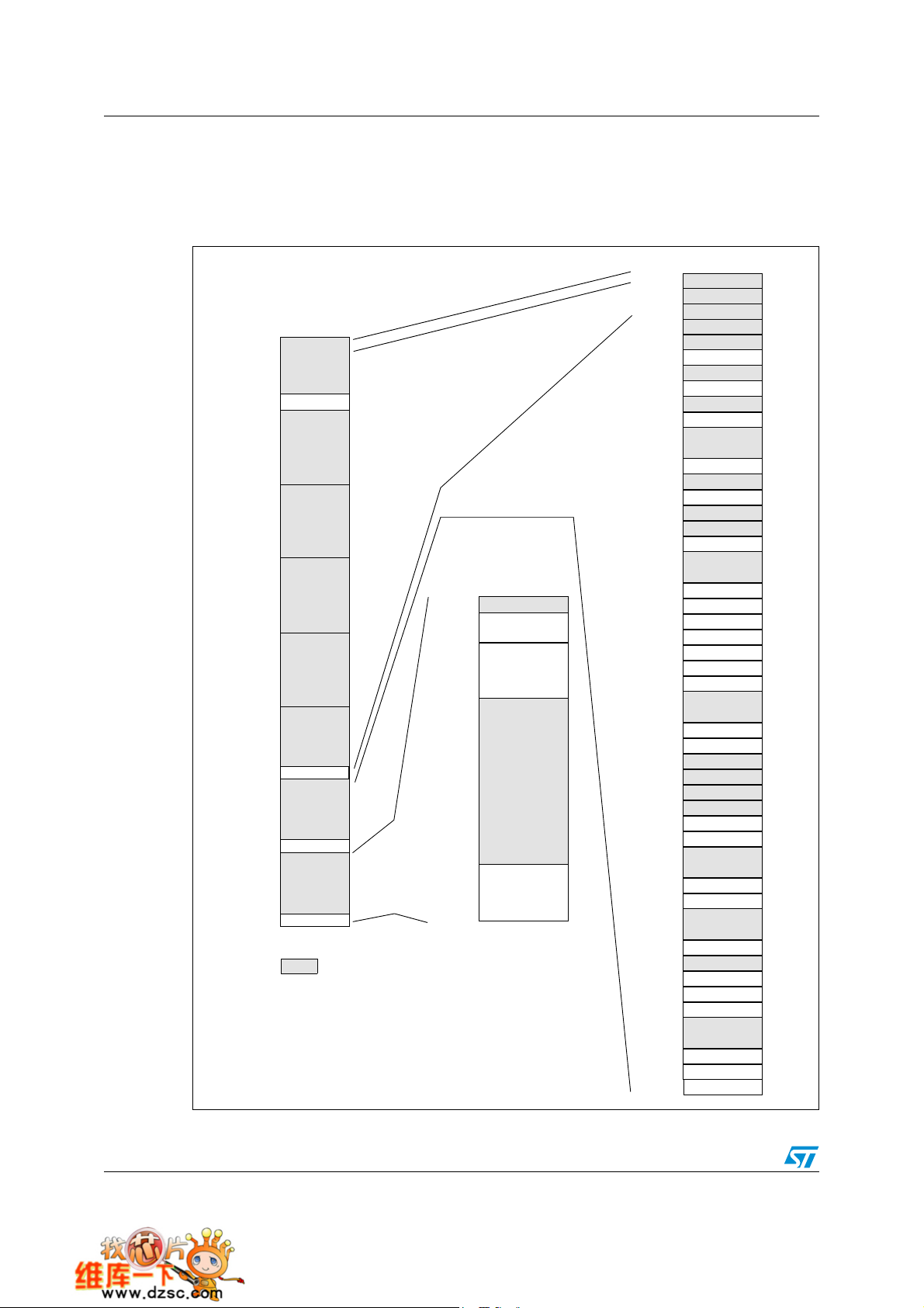
Figure 1 shows the general block diagram of the device family.
6/64

STM32F101xx Description
2.1 Device overview
Table 2. Device features and peripheral counts (STM32F101xx access line)
Peripheral
Flash - Kbytes 32 64 32 64 128 64 128
SRAM - Kbytes 610610161016
General purpose 23 3 3
Timers
SPI 121 2 2
2
C 121 2 2
I
USART 232 3 3
Communication
12-bit synchronized ADC
number of channels
GPIOs 32 49 80
STM32F101Cx STM32F101Rx STM32F101Vx
1
10 channels
1
16 channels
CPU frequency 36 MHz
Operating voltage 2.0 to 3.6 V
Operating temperature -40 to +85 °C
Packages LQFP48 LQFP64 LQFP100
7/64

Description STM32F101xx
2.2 Overview
ARM® CortexTM-M3 core with embedded Flash and SRAM
The ARM Cortex™-M3 processor is the latest generation of ARM processors for embedded
systems. It has been de v eloped t o prov ide a low- cost platform that meets the needs of MCU
implementation, with a reduced pin count and low-power consumption, while delivering
outstanding computational performance and an advanced system response to interrupts.
The ARM Cortex™-M3 32-bit RISC processor features exceptional code-efficiency,
delivering the high-performance expected from an ARM core in the memory size usually
associated with 8- and 16-bit devices.
The STM32F101xx access line family having an embedded ARM core, is therefore
compatible with all ARM tools and software.
Embedded Flash memory
Up to 128 Kbytes of embedded Flash is available for storing programs and data.
Embedded SRAM
Up to 16 Kbytes of embedded SRAM accessed (read/write) at CPU clock speed with 0 wait
states.
Nested vectored interrupt controller (NVIC)
The STM32F101xx access line embeds a nested vectored interrupt controller able to handle
up to 43 maskable interrupt channels (not including the 16 interrupt lines of Cortex™-M3)
and 16 priority levels.
● Closely coupled NVIC gives low latency interrupt processing
● Interrupt entry vector table address passed directly to the core
● Closely coupled NVIC core interface
● Allows early processing of interrupts
● Processing of late arriving higher priority inte r rupts
● Support for tail-chaining
● Processor state automatically saved
● Interrupt entry restored on interrupt exit with no instruction overhead
This hardware block provides flexible interrupt management features with minimal interrupt
latency.
8/64

STM32F101xx Description
External interrupt/event controller (EXTI)
The external interrupt/event controller consists of 19 edge detectors lines used to generate
interrupt/event requests. Each line can be independently configured to select the trigger
event (rising edge , falling edge, both) and ca n be mask ed ind ependently. A pending register
maintains the status of the interrupt requests. The EXTI can detect external line with pulse
width lower than the Internal APB2 clock period. Up to 80 GPIOs are connected to the 16
external interrupt lines.
Clocks and startup
System clock selection is performed on startup, however the internal RC 8 MHz oscillator is
selected as default CPU clock on reset. An external 4-16 MHz clock can be selected and is
monitored for failure. During such a scenario, it is disabled and software interrupt
management follo ws . Similarly, full interrupt management of the PLL clock entry is av ailable
when necessary (for example with failure of an indirectly used external oscillator).
Several prescalers allow the configuration of the AHB frequency, the High Speed APB
(APB2) and the low Speed APB (APB1) domains. The maximum frequency of the AHB and
the APB domains is 36 MHz.
Boot modes
At startup, boot pins are used to select one of five boot options:
● Boot from User Flash
● Boot from System Memory
● Boot from SRAM
The boot loader is located in System Memory. It is used to reprogram the Flash memory by
using the USART.
Power supply schemes
● V
● V
● V
= 2.0 to 3.6 V: External power sup ply for I/Os and the internal regulator.
DD
Provided externally through V
, V
SSA
and PLL. In V
BAT
= 2.0 to 3.6 V: External analog power sup plies for ADC, Reset b loc ks , RCs
DDA
range (ADC is limited at 2.4 V).
DD
= 1.8 to 3.6 V: Power supply for RTC, external clock 32 kHz oscillator and backup
registers (through power switch) when V
DD
pins.
is not present.
DD
Power supply supervisor
The device has an integrated power on reset (POR)/power down reset (PDR) circuitry. It is
always active, and ensures proper operation starting from/down to 2 V. The device remains
in reset mode when V
external reset circuit.
The device features an embedded Programmable voltage detector (PVD) that monitors the
V
power supply and compares it to the V
DD
when V
drops below the V
DD
interrupt service routine can then generate a warning message and/or put the MCU into a
safe state. The PVD is enabled by software.
Refer to Table 9: Embedded reset and power control block characteristics for the values of
V
POR/PDR
and V
PVD
is below a specified threshold, V
DD
and/or when VDD is higher than the V
PVD
PVD
.
POR/PDR
, without the need for an
threshold. An interrupt can be generated
threshold. The
PVD
9/64

Description STM32F101xx
Voltage regulator
The regulator has three operation modes: ma in (M R ), low power (LPR) and power down.
● MR is used in the nominal regulation mode (Run)
● LPR is used in the Stop modes
● Power down is used in Standby Mode: the regulator output is in high impedance: the
kernel circuitry is powered-down, inducing zero consumption (but the contents of the
registers and SRAM are lost)
This regulator is always enabled after RESET. It is disabled in Standby Mode, providing high
impedance output.
Low-power modes
The STM32F101xx access line supports three low-power modes to achieve the best
compromise between low power consumption, short startup time and available wakeup
sources:
● Sleep mode
In Sleep mode, only the CPU is stopped. All peripherals continue to operate and can
wake up the CPU when an interrupt/event occurs.
● Stop mode
Stop mode allows to achieve the lowest po we r consumption while re taining the co ntent
of SRAM and registers. All clocks in the 1.8 V domain are stopped, the PLL, the HSI
and the HSE RC oscillators are disabled. The voltage regulator can also be put either in
normal or in low power mode.
The device can be wok en up from Stop mode by any of the EXTI line. The EXTI line
source can be one of the 16 external lines, the PVD output or the RTC alarm.
● Standby mode
The Standby mode allows to achieve the lo west power consumption. The internal
voltage regulator is switched off so that the entire 1.8 V domain is powered off. The
PLL, the HSI and the HSE RC oscillators are also switched off. After entering Standby
mode, SRAM and registers content are lost except for registers in the Backup domain
and Standby circuitry.
The device exits Standby mode when an external reset (NRST pin), a IWDG reset, a
rising edge on the WKUP pin, or an RTC alarm occurs.
Note: The RTC , the IWDG, and t he corresponding cloc k sources ar e not stopped by e ntering Stop
or Standby mode.
DMA
The flexible 7-channel general-purpose DMA is able to manage memory-to-memory,
peripheral-to-memory and memory-to-peripheral transfers. The DMA controller supports
circular buffer management avoiding the generation of interrupts when the controller
reaches the end of the buffer.
Each channel is connected to dedicated hardware DMA requests, with support for software
trigger on each channel. Configuration is made by software and transfer sizes between
source and destination are independent.
The DMA can be used with the main peripherals: SPI, I
TIMx and ADC.
10/64
2
C, USART, general purpose timers

STM32F101xx Description
RTC (real-time clock) and backup registers
The RTC and the bac kup registers are supplied through a switch that takes po wer either on
V
supply when present or through the V
DD
can be used to store data when V
power is not present.
DD
pin. The backup registers (ten 16-bit registers)
BAT
The Real-Time Clock provides a set of continuously running counters which can be used
with suitable software to provide a clock calendar function, and provides an alarm interrupt
and a periodic interrupt. It is clocked by an external 32.768 kHz oscillator, the internal low
power RC oscillator or the high-speed external clock divided by 128. The internal low pow er
RC has a typical frequency of 32 kHz. The RTC can be calibrated using an external 512Hz
output to compensate for any natural quartz deviation. The RTC features a 32-bit
programmable counter for long term measurement using the Compare register to generate
an alarm. A 20-bit prescaler is used for the time base clock and is by default configured to
generate a time base of 1 second from a clock at 32.768 kHz.
Independent watchdog
The independent watchdog is based on a 12-bit downcounter and 8-bit prescaler. It is
clocked from an independent 32 kHz internal RC and as it operates independently from the
main clock, it can operate in Stop and Standby modes. It can be used as a watchdog to
reset the device when a problem occurs, or as a free running timer for application time out
management. It is hardware o r software configurable through the option bytes. The counter
can be frozen in debug mode.
Window watchdog
The window watchdog is based on a 7-bit downcounter that can be set as free running. It
can be used as a watchdog to reset the de vice when a prob lem occurs . It is clock ed from the
main clock. It has an early warning interrupt capability and the counter can be frozen in
debug mode.
SysTick timer
This timer is dedicated for OS, but could also be used as a standard down counter. It
features:
● A 24-bit down counter
● Autoreload capability
● Maskable system interrupt generation whe n th e co un te r re ach e s 0.
● Programmable clock source
General purpose timers (TIMx)
There are up to 3 synchronizable standard timers embedded in the STM32F101xx access
line devices. These timers are based on a 16-bit auto-reload up/down counter, a 16-bit
prescaler and feature 4 in dependent channels each f or input captu re, output compa re, PWM
or one pulse mode output. This give s u p to 12 input ca ptur es / o utpu t compar es / PWMs on
the largest packages. They can work together via the Timer Link feature for synchronization
or event chaining.
The counter can be frozen in debug mode.
Any of the standard timers can be used to generate PWM outputs. Each of the timers has
independent DMA request generations.
11/64

Description STM32F101xx
I²C bus
Up to two I²C bus interf aces can oper ate in multi-maste r and slav e modes . They can sup port
standard and fast modes.
They support dual slave addressing (7-bit only) and both 7/10-bit addressing in master
mode. A hardware CRC generation/verification is embedded.
They can be served by DMA and they support SM Bus 2.0/PM Bus.
Universal synchronous/asynchronous receiver transmitter (USART)
The available USART interfaces communicate at up to 2.25 Mbit/s. They provide hardware
management of the CTS and RTS signals, support IrDA SIR ENDEC, are ISO 7816
compliant and have LIN Master/Slave capability.
The USART interfaces can be served by the DMA controller.
Serial peripheral interface (SPI)
Up to two SPIs are able to communicate up to 18 Mbits/s in slave and master modes in fullduplex and simplex communication modes. The 3-bit prescaler gives 8 master mode
frequencies and the frame is configurable from 8-bit to 16-bit. The hardware CRC
generation/ve rification supports basic SD Card/MMC modes.
Both SPIs can be served by the DMA controller.
GPIOs (general purpose inputs/outputs)
Each of the GPIO pins can be configured b y softw are as output ( push-pull or open-dr ain), as
input (with or without pull-up or pull-down) or as Peripheral Alternate Function. Most of the
GPIO pins are shared with digital or analog alternate functions. All GPIOs are high currentcapable.
The I/Os alternate function configuration can be locked if needed following a specific
sequence in order to avoid spurious writing to the I/Os registers.
ADC (analog to digital converter)
The 12-bit Analog to Digital Converter has up to 16 external channels and performs
conversions in single-shot or scan modes. In scan mode, automatic conversion is performed
on a selected group of analog inputs.
The ADC can be served by the DMA controller.
An analog watchdog f eatur e allo ws very precise monitoring of the converted voltage of one ,
some or all selected channels. An interrupt is generated when the converted voltage is
outside the programmed thresholds.
Temperature sensor
The temperature sensor has to generate a linear voltage with any variation in temperature.
The conversion range is between 2V < V
connected to the ADC_IN16 input channel which is used to convert the sensor output
voltage into a digital value.
< 3.6V. The temperature sensor is internally
DDA
12/64
STM32F101xx Description
Serial wire JTAG debug port (SWJ-DP)
The ARM SWJ-DP Interface is embedded. and is a combined JTAG and serial wire debug
port that enables either a serial wire debug or a JTAG probe to be connected to the target.
The JTAG TMS and TCK pins are shared respectively with SWDIO and SWCLK and a
specific sequence on the TMS pin is used to switch between JTAG-DP and SW-DP.
Figure 1. STM32F101xx access line block diagram
JNTRST
JTDI
JTCK/SWCLK
JTMS/SWDIO
JTDO
as AF
80AF
PA[15:0]
PB[15:0]
PC[15:0]
PD[15:0]
PE[15:0]
MOSI,MISO,
SCK,NSS as AF
RX,TX, CTS, RTS,
SmartCard as AF
16AF
V
REF+
V
REF-
NRST
VDDA
VSSA
JTAG & SWD
Cortex M3 CPU
F
max
NVIC
NVIC
7 channels
SUPERVISION
POR / PDR
EXTI
WAKEUP
GPIOA
GPIOB
GPIOC
GPIOD
GPIOE
SPI1
USART1
@VDDA
12bit ADC1
Temp sensor
: 36 MHz
GP DMA
@VDDA
SUPPLY
PVD
IF
pbus
Dbus
System
Rst
Int
Ibus
= 36 MHz
max
APB2 : F
BusMatrix
Controller
AHB2
APB2
Trace
=36 MHz
max
AHB:F
obl
FLASH 128 KB
Interface
Flash
SRAM
16 KB
PCLK1
PCLK2
HCLK
FCLK
RC 8 MHz
RC 32 kHz
@VDDA
AHB2
APB1
64 bit
CLOCK
MANAGT
PLL &
=24 / 36 MHz
max
APB1 : F
@VBAT
Backup interface
2x(8x16bit)
POWER
VOLT. REG.
3.3V TO 1.8V
@VDD
@VDD
XTAL OSC
4-16 MHz
IWDG
Standby
interface
XTAL 32 kHz
Backup
RTC
AWU
TIM2
TIM3
TIM4
USART2
USART3
SPI2
I2C1
I2C2
W W D G
reg
V
= 2 to 3.6V
DD
V
SS
OSC_IN
OSC_OUT
V
BAT
OSC32_IN
OSC32_OUT
ANTI_TAMP
4 Channels
4 Channels
4 Channels
RX,TX, CTS, RTS,
SmartCard as AF
RX,TX, CTS, RTS,
SmartCard as AF
MOSI,MISO,SCK,NSS
as AF
SCL,SDA,SMBAL
as AF
SCL,SDA
as AF
1. AF = alternate function on I/O port pin.
2. TA = –40 °C to +85 °C (junction temperature up to 125 °C).
13/64
ai14385
Pin descriptions STM32F101xx
3 Pin descriptions
Figure 2. STM32F101xx access line LQFP100 pinout
VDD_3
VSS_3
PE1
PE0
PB9
PB8
BOOT0
PB7
PB6
PB5
PB4
PB3
PD7
PD6
PD5
PD4
PD3
PD2
PD1
PD0
PC12
PC11
PC10
PA15
PA14
PE2
PE3
PE4
PE5
PE6
VBAT
PC13-ANTI_TAMP
PC14-OSC32_IN
PC15-OSC32_OUT
VSS_5
VDD_5
OSC_IN
OSC_OUT
NRST
PC0
PC1
PC2
PC3
VSSA
VREF-
VREF+
VDDA
PA0-WKUP
PA1
PA2
100999897969594939291908988878685848382818079787776
1
2
3
4
5
6
7
8
9
10
11
12
13
14
15
16
17
18
19
20
21
22
23
24
25
26272829303132333435363738394041424344454647484950
PA3
PA4
PA5
PA6
PA7
VSS_4
VDD_4
PC4
PC5
PB0
LQFP100
PB1
PB2
PE7
PE8
PE9
PE10
PE11
PE12
PE13
PE14
PE15
PB10
PB11
VSS_1
75
VDD_2
74
VSS_2
73
NC
72
PA 13
71
PA 12
70
PA 11
69
PA 10
68
PA 9
67
PA 8
66
PC9
65
PC8
64
PC7
63
PC6
62
PD15
61
PD14
60
PD13
59
PD12
58
PD11
57
PD10
56
PD9
55
PD8
54
PB15
53
PB14
52
PB13
51
PB12
VDD_1
14/64
ai14386
STM32F101xx Pin descriptions
Figure 3. STM32F101xx access line LQFP64 pinout
VDD_3
VSS_3
PB9
PB8
BOOT0
PB7
PB6
PB5
PB4
PB3
PD2
PC12
PC11
PC10
PA15
PA14
PC13-ANTI_T AMP
VBAT
PC14-OSC32_IN
PC15-OSC32_OUT
PD0 OSC_IN
PD1 OSC_OUT
NRST
PC0
PC1
PC2
PC3
VSSA
VDDA
PA0-WKUP
PA1
PA2
64 63 62 61 60 59 58 57 56 55 54 53 52 51 50 49
1
2
3
4
5
6
7
8
9
10
11
12
13
14
15
16
17 18 19 20 21 22 23 24 29 30 31 3225 26 27 28
PA3
VSS_4
VDD_4
PA4
PA5
PA6
LQFP64
PA7
PC4
PC5
PB0
PB1
PB2
PB10
PB11
VDD_2
48
VSS_2
47
PA13
46
PA12
45
PA11
44
PA10
43
PA9
42
PA8
41
PC9
40
PC8
39
PC7
38
PC6
37
PB15
36
PB14
35
PB13
34
33
PB12
VSS_1
VDD_1
Figure 4. STM32F101xx access line LQFP48 pinout
VDD_3
VSS_3
PB9
PB8
BOOT0
PB7
PB6
PB5
PB4
PB3
PC13-ANTI_TAMP
VBAT
PC14-OSC32_IN
PC15-OSC32_OUT
PD0 OSC_IN
PD1 OSC_OUT
NRST
VSSA
VDDA
PA0-WKUP
PA1
PA2
48 47 46 45
1
2
3
4
5
6
7
8
9
10
11
12
13 14 15 16 17 18
PA3
44 43 42 41 40 39 38 37
LQFP48
19 20 21 22
PA4
PA5
PA6
PA7
PB0
PB1
PB2
PB10
23
PB11
VSS_1
ai14387
PA15
PA14
VDD_2
36
VSS_2
35
PA13
34
PA12
33
PA11
32
PA10
31
PA9
30
PA8
29
PB15
28
PB14
27
26
PB13
25
PB12
24
VDD_1
ai14378
15/64
Pin descriptions STM32F101xx
LQFP64
(2)
(1)
Pin name
Type
LQFP100
SV
BAT
(4)
(4)
(4)
SS_5
DD_5
I/O PC13 ANTI_TAMP
I/O
I/O
SV
SV
I / O level
FT
FT
FT
FT
FT
Main
function
(after reset)
PE2 TRACECK
PE3 TRACED0
PE4 TRACED1
PE5 TRACED2
PE6 TRACED3
PC14-
OSC32_IN
PC15-
OSC32_OUT
Table 3. Pin definitions
Pins
LQFP48
- - 1 PE2/TRACECK I/O
- - 2 PE3/TRACED0 I/O
- - 3 PE4/TRACED1 I/O
- - 4 PE5/TRACED2 I/O
- - 5 PE6/TRACED3 I/O
11 6 V
2 2 7 PC13-ANTI_TAMP
3 3 8 PC14-OSC32_IN
4 4 9 PC15-OSC32_OUT
--10 V
--11 V
5 5 12 OSC_IN I OSC_IN
BAT
SS_5
DD_5
(3)
Default alternate functions
(3)
6 6 13 OSC_OUT O OSC_OUT
7 7 14 NRST I/O NRST
- 8 15 PC0/ADC_IN10 I/O PC0 ADC_IN10
- 9 16 PC1/ADC_IN11 I/O PC1 ADC_IN11
- 10 17 PC2/ADC_IN12 I/O PC2 ADC_IN12
- 11 18 PC3/ADC_IN13 I/O PC3 ADC_IN13
81219 V
SSA
SV
SSA
- - 20 VREF- S VREF-
- - 21 VREF+ S VREF+
91322 V
10 14 23
11 15 24
12 16 25
13 17 26
PA0-WKUP/USART2_CTS/
ADC_IN0/TIM2_CH1_ETR
PA1/USART2_RTS/ADC_
PA2/USART2_TX/ADC_IN2/
PA3/USART2_RX/ADC_IN3/
-1827 V
-1928 V
DDA
IN1/TIM2_CH2
TIM2_CH3
TIM2_CH4
SS_4
DD_4
SV
I/O PA0
DDA
WKUP/USART2_CTS
I/O PA1
I/O PA2
I/O PA3
SV
SV
SS_4
DD_4
TIM2_CH1_ETR
USART2_RTS
TIM2_CH2
USART2_TX
TIM2_CH3
USART2_RX
TIM2_CH4
(7)
/ ADC_IN0/
(7)
/ADC_IN1/
(7)
(7)
/ADC_IN2/
(7)
(7)
/ADC_IN3/
(7)
(7)
16/64
STM32F101xx Pin descriptions
Table 3. Pin definitions (continued)
Pins
LQFP48
LQFP64
14 20 29
Pin name
LQFP100
PA4/SPI1_NSS/
USART2_CK/ADC_IN4
I/O PA4
(1)
(2)
Type
Main
function
(3)
(after reset)
Default alternate functions
I / O level
SPI1_NSS/USART2_CK
ADC_IN4
15 21 30 PA5/SPI1_SCK/ADC_IN5 I/O PA5 SPI1_SCK/ADC_IN5
16 22 31
17 23 32
PA6/SPI1_MISO/ADC_IN6/
TIM3_CH1
PA7/SPI1_MOSI/ADC_IN7/
TIM3_CH2
I/O PA6
I/O PA7
SPI1_MISO/ADC_IN6/
TIM3_CH1
SPI1_MOSI/ADC_IN7/
TIM3_CH2
(7)
(7)
- 24 33 PC4/ADC_IN14 I/O PC4 ADC_IN14
- 25 34 PC5/ADC_IN15 I/O PC5 ADC_IN15
18 26 35 PB0/ADC_IN8/TIM3_CH3 I/O PB0 ADC_IN8/TIM3_CH3
19 27 36 PB1/ADC_IN9/TIM3_CH4 I/O PB1 ADC_IN9/TIM3_CH4
(7)
(7)
20 28 37 PB2/BOOT1 I/O FT PB2/BOOT1
- - 38 PE7 I/O FT PE7
- - 39 PE8 I/O FT PE8
- - 40 PE9 I/O FT PE9
(7)
(3)
/
- - 41 PE10 I/O FT PE10
- - 42 PE11 I/O FT PE11
- - 43 PE12 I/O FT PE12
- - 44 PE13 I/O FT PE13
- - 45 PE14 I/O FT PE14
- - 46 PE15 I/O FT PE15
21 29 47
22 30 48
PB10/I2C2_SCL
USART3_TX
PB11/I2C2_SDA
USART3_RX
23 31 49 V
24 32 50 V
25 33 51
26 34 52
27 35 53
PB12/SPI2_NSS/
I2C2_SMBAl/USART3_CK
PB13/SPI2_SCK/
USART3_CTS
PB14/SPI2_MISO/
USART3_RTS
SS_1
DD_1
I/O FT PB10 I2C2_SCL
I/O FT PB11 I2C2_SDA
SV
SV
I/O FT PB12
SS_1
DD_1
SPI2_NSS
I/O FT PB13 SPI2_SCK
I/O FT PB14 SPI2_MISO
(5)
/USART3_TX
(5)
/USART3_RX
(5) (7)
/I2C2_SMBAl
USART3_CK
(5)(7)
/USART3_CTS
(5)(7)
/USART3_RTS
28 36 54 PB15/SPI2_MOSI I/O FT PB15 SPI2_MOSI
- - 55 PD8 I/O FT PD8
(5) (7)
(5) (7)
(5) (7)
(5) (7)
(5)
(5)(7)
(5)(7)
/
17/64

Pin descriptions STM32F101xx
Table 3. Pin definitions (continued)
LQFP48
Pins
LQFP64
Pin name
LQFP100
(1)
(2)
Type
Main
function
(3)
(after reset)
Default alternate functions
I / O level
- - 56 PD9 I/O FT PD9
- - 57 PD10 I/O FT PD10
- - 58 PD11 I/O FT PD11
- - 59 PD12 I/O FT PD12
- - 60 PD13 I/O FT PD13
- - 61 PD14 I/O FT PD14
- - 62 PD15 I/O FT PD15
- 37 63 PC6 I/O FT PC6
38 64 PC7 I/O FT PC7
39 65 PC8 I/O FT PC8
- 40 66 PC9 I/O FT PC9
29 41 67 PA8/USART1_CK/MCO I/O FT PA8 USART1_CK/MCO
30 42 68 PA9/USART1_TX I/O FT PA9 USART1_TX
31 43 69 PA10/USART1_RX I/O FT PA10 USART1_RX
(7)
(7)
32 44 70 PA11/USART1_CTS I/O FT P A11 USART1_CTS
(3)
33 45 71 PA12/USART1_RTS I/O FT PA12 USART1_RTS
34 46 72 PA13/JTMS/SWDIO I/O FT JTMS-SWDIO PA13
- - 73 Not connected
35 47 74 V
36 48 75 V
SS_2
DD_2
SV
SV
SS_2
DD_2
37 49 76 PA14/JTCK/SWCLK I/O FT JTCK/SWCLK PA14
38 50 77 PA15/JTDI I/O FT JTDI PA15
-5178 PC10 I/OFT PC10
-5279 PC11 I/OFT PC11
-5380 PC12 I/OFT PC12
5 5 81 PD0 I/O FT OSC_IN
6 6 82 PD1 I/O FT OSC_OUT
(6)
(6)
54 83 PD2/TIM3_ETR I/O FT PD2 TIM3_ETR
- - 84 PD3 I/O FT PD3
- - 85 PD4 I/O FT PD4
- - 86 PD5 I/O FT PD5
- - 87 PD6 I/O FT PD6
18/64
STM32F101xx Pin descriptions
Table 3. Pin definitions (continued)
LQFP48
Pins
LQFP64
Pin name
LQFP100
(1)
(2)
Type
Main
function
(3)
(after reset)
Default alternate functions
(3)
I / O level
- - 88 PD7 I/O FT PD7
39 55 89 PB3/JTDO/TRACESWO I/O FT JTDO PB3/TRACESWO
40 56 90 PB4/JNTRST I/O FT JNTRST PB4
41 57 91 PB5/I2C1_SMBAl I/O PB5 I2C1_SMBAl
42 58 92 PB6/I2C1_SCL/TIM4_CH1 I/O FT PB6 I2C1_SCL
43 59 93 PB7/I2C1_SDA/TIM4_CH2 I/O FT PB7 I2C1_SDA
(7)
/TIM4_CH1
(7)
/TIM4_CH2
(5) (7)
(5) (7)
44 60 94 BOOT0 I BOOT0
45 61 95 PB8/TIM4_CH3 I/O FT PB8 TIM4_CH3
46 62 96 PB9/TIM4_CH4 I/O FT PB9 TIM4_CH4
- - 97 PE0/TIM4_ETR I/O FT PE0 TIM4_ETR
(5) (7)
(5) (7)
(5)
- - 98 PE1 I/O FT PE1
47 63 99 V
48 64 100 V
1. I = input, O = output, S = supply, HiZ= high impedance.
2. FT= 5 V tolerant.
3. Function availability depends on the chosen device. Refer to Table 2 on page 7.
4. PC13, PC14 and PC15 are supplied through the power switch, and so their use in ouptut mode is limited: they can be used
only in output 2 MHz mode with a maximum load of 30 pF and only one pin can be put in output mode at a time.
5. Available only on devices with a Flash memory density equal or higher than 64 Kbytes.
6. For the LQFP48 and LQFP64 packages, the pins number 5 and 6 are configured as OSC_IN/OSC_OUT after reset,
however the functionality of PD0 and PD1 can be remapped by software on these pins.
7. This alternate function can be remapped by software to some other port pins (if available on the used package). For more
details, refer to the Alternate function I/O and debug configuration section in the STM32F10xxx reference manual,
UM0306, available from the STMicroelectronics website: www.st.com.
SS_3
DD_3
SV
SV
SS_3
DD_3
19/64
Memory mapping STM32F101xx
4 Memory mapping
The memory map is shown in Figure 5.
Figure 5. Memory map
APB memory space
0xFFFF FFFF
0xFFFF F000
7
0xE010 0000
0xE000 0000
6
0xC000 0000
5
0xA000 0000
4
0x8000 0000
3
0x6000 0000
2
0x4000 0000
1
0x2000 0000
0
0x0000 0000
ai14379
Cortex-M3 internal
peripherals
Peripherals
SRAM
Code
Reserved
0x1FFF FFFF
0x1FFF F9FF
0x1FFF F800
0x1FFF F000
0x0801 FFFF
0x0800 0000
reserved
Option bytes
System memory
reserved
Flash memory
0xFFFF FFFF
0xE010 0000
0x6000 0000
0x4002 3400
0x4002 3000
0x4002 2400
0x4002 2000
0x4002 1400
0x4002 1000
0x4002 0400
0x4002 0000
0x4001 3C00
0x4001 3800
0x4001 3400
0x4001 3000
0x4001 2C00
0x4001 2800
0x4001 2400
0x4001 1C00
0x4001 1800
0x4001 1400
0x4001 1000
0x4001 0C00
0x4001 0800
0x4001 0400
0x4001 0000
0x4000 7400
0x4000 7000
0x4000 6C00
0x4000 6800
0x4000 6400
0x4000 6000
0x4000 5C00
0x4000 5800
0x4000 5400
0x4000 4C00
0x4000 4800
0x4000 4400
0x4000 3C00
0x4000 3800
0x4000 3400
0x4000 3000
0x4000 2C00
0x4000 2800
0x4000 0C00
0x4000 0800
0x4000 0400
0x4000 0000
reserved
reserved
reserved
reserved
reserved
Flash interface
reserved
RCC
reserved
DMA
reserved
USART1
reserved
SPI1
reserved
reserved
ADC1
reserved
Port E
Port D
Port C
Port B
Port A
EXTI
AFIO
reserved
PWR
BKP
reserved
reserved
reserved
reserved
I2C2
I2C1
reserved
USART3
USART2
reserved
SPI2
reserved
IWDG
WWDG
RTC
reserved
TIM4
TIM3
TIM2
4K
1K
3K
1K
3K
1K
3K
1K
1K
1K
1K
1K
1K
1K
1K
2K
1K
1K
1K
1K
1K
1K
1K
35K
1K
1K
1K
1K
1K
1K
1K
1K
2K
1K
1K
2K
1K
1K
1K
1K
1K
7K
1K
1K
1K
20/64

STM32F101xx Electrical characteristics
5 Electrical characteristics
5.1 Test conditions
Unless otherwise specified, all voltages are referred to VSS.
5.1.1 Minimum and maximum values
Unless otherwise specified the minimum and maximum values are guaranteed in the worst
conditions of ambient temperature , supply v olta ge and frequ encies b y tests in production on
100% of the devices with an ambient temperature at T
the selected temperature range ).
Data based on characterization results, design simulation and/or technology characteristics
are indicated in the table footnotes and are not tested in production. Based on
characterization, the minimum and maximum v alu es ref er to sample tests an d represent th e
mean value plus or minus three times the standard deviation (mean±3Σ).
5.1.2 Typical values
= 25 °C and TA = TAmax (given by
A
Unless otherwise specified, typical data are based on TA = 25 °C, V
2V≤V
tested.
Typical ADC accuracy values are determined by characterizati on of a batch of samples fr om
a standard diffusion lot over the full temperature range, where 95% of the devices have an
error less than or equal to the value indicated
≤3.6 V voltage range). They are given only as design guidelines and are not
DD
5.1.3 Typical curves
Unless otherwise specified, all typical curves are given only as design guidelines and are
not tested.
5.1.4 Loading capacitor
The loading conditions used for pin parameter measurement are shown in Figure 6.
5.1.5 Pin input voltage
The input voltage measurement on a pi n of the device is described in Figure 7.
(mean±2Σ).
= 3.3 V (for the
DD
21/64

Electrical characteristics STM32F101xx
Figure 6. Pin loading conditions Figure 7. Pin input voltage
C=50pF
5.1.6 P ower supply scheme
Figure 8. Power supply scheme
1.8-3.6V
V
DD
5 × 100 nF
+ 1 × 10 µF
V
DD
V
REF
10 nF
+ 1 µF
10 nF
+ 1 µF
STM32F101 PIN
ai14123
V
GP I/Os
V
1/2/3/4/5
1/2/3/4/5
BAT
V
3.3 V
DD
SS
3.3V
V
DDA
V
REF+
V
REF-
V
SSA
Power switch
OUT
IN
Regulator
ADC
Backup circuitry
(OSC32K,RTC,
Wake-up logic
Backup registers)
IO
Logic
Level shifter
Analog:
RCs, PLL,
...
V
IN
STM32F101 PIN
ai14124
Kernel logic
(CPU,
Digital
& Memories)
ai14125
22/64

STM32F101xx Electrical characteristics
5.1.7 Current consumption measurement
Figure 9. Current consumption measurement scheme
IDD_V
BAT
V
BAT
I
DD
V
DD
V
DDA
ai14126
23/64

Electrical characteristics STM32F101xx
5.2 Absolute maximum ratings
Stresses above the absolute maximum ratings listed in Table 4: Voltage characteristics,
Table 5: Current characteristics, and T able 6: Thermal characteristics may cause permanent
damage to the device. These are stress ratings only and functional operation of the device
at these conditions is not implied. Exposure to maximum rating conditions for extended
periods may affect device reliability.
Table 4. Voltage characteri stics
Symbol Ratings Min Max Unit
VDD−V
V
IN
|∆V
DDx
|V
− VSS|
SSX
V
ESD(HBM)
1. All 3.3 V power (VDD, V
supply.
2. I
INJ(PIN)
maximum is respected. If V
externally to the I
induced by VIN<VSS.
Table 5. Current characteristics
External 3.3 V supply voltage (including
SS
V
and VDD)
DDA
(1)
Input voltage on five volt tolerant pin
Input voltage on any other pin
(2)
(2)
−0.3 4.0
V
− 0.3 +5.5
SS
VSS − 0.3 VDD+0.3
| Variations between different power pins 50 50
Variations between all the different ground
pins
Electrostatic discharge voltage (human
body model)
) and ground (VSS, V
DDA
must never be exceeded (see Table 5: Current characteristics). This is implicitly insured if VIN
INJ(PIN)
maximum cannot be respected, the injection current must be limited
IN
value. A positive injection is induced by VIN>VDD while a negative injection is
) pins must always be connected to the external 3.3 V
SSA
50 50
see Section 5.3.11: Absolute
maximum ratings (electrical
sensitivity)
mV
Symbol Ratings Max. Unit
I
VDD
I
VSS
Total current into V
DD
Total current out of V
power lines (source)
ground lines (sink)
SS
(1)
(1)
150
150
Output current sunk by any I/O and control pin 25
I
IO
Output current source by any I/Os and control pin − 25
Injected current on NRST pin ± 5
(2)(3)
I
INJ(PIN)
ΣI
INJ(PIN)
1. All 3.3 V power (VDD, V
supply.
2. I
3. Negative injection disturbs the analog performance of the device. See note in Section 5.3.16: 12-bit ADC
4. When several inputs are submitted to a current injection, the maximum ΣI
must never be exceeded. This is implicitly insured if VIN maximum is respected. If VIN maximum
INJ(PIN)
cannot be respected, the injection current must be limited externally to the I
injection is induced by VIN>VDD while a negative injection is induced by VIN<VSS.
characteristics.
positive and negative injected currents (instantaneous values). These results are based on
characterization with ΣI
Injected current on High-speed external OSC_IN and Lowspeed external OSC_IN pins
Injected current on any other pin
(2)
Total injected current (sum of all I/O and control pins)
) and ground (VSS, V
DDA
maximum current injection on four I/O port pins of the device.
INJ(PIN)
(4)
) pins must always be connected to the external 3.3 V
SSA
(4)
INJ(PIN)
is the absolute sum of the
INJ(PIN)
± 25
value. A positive
± 5
± 5
V
mA
24/64

STM32F101xx Electrical characteristics
Table 6. Thermal characteristics
Symbol Ratings Value Unit
T
STG
T
J
Storage temperature range –65 to +150 °C
Maximum junction temperature (see Thermal characteristics)
25/64

Electrical characteristics STM32F101xx
5.3 Operating conditions
5.3.1 General operating conditions
Table 7. General operating conditions
Symbol Parameter Conditions Min Max Unit
f
HCLK
PCLK1
f
PCLK2
V
DD
V
BAT
T
A
Internal AHB clock frequency 0 36
Internal APB1 clock frequency 0 36
Internal APB2 clock frequency 0 36
Standard operating voltage 2 3.6 V
Backup operating voltage 1.8 3.6 V
Ambient temperature range −40 85 °C
5.3.2 Operating conditions at power-up / power-down
The parameters given in Table 8 are derived from tests performed under the ambient
temperature condition summarized in Table 7.
Table 8. Operating conditions at power-up / power-down
Symbol Parameter Conditions Min Typ Max Unit
t
VDD
VDD rise/fall time
MHzf
20 µs/V
20 ms/V
26/64

STM32F101xx Electrical characteristics
5.3.3 Embedded reset and power control block characteristics
The parameters given in Table 9 are derived from tests performed under ambient
temperature and V
.
Table 9. Embedded reset and power control block characteristics
Symbol Parameter Conditions Min Typ Max Unit
supply voltage conditions summarized in Table 7.
DD
PLS[2:0]=000 (rising edge) 2.1 2.18 2.26 V
PLS[2:0]=000 (falling edge) 2 2.08 2.16 V
PLS[2:0]=001 (rising edge) 2.19 2.28 2.37 V
PLS[2:0]=001 (falling edge) 2.09 2.18 2.27 V
PLS[2:0]=010 (rising edge) 2.28 2.38 2.48 V
PLS[2:0]=010 (falling edge) 2.18 2.28 2.38 V
PLS[2:0]=011 (rising edge) 2.38 2.48 2.58 V
V
PVD
V
PVDhyst
V
POR/PDR
V
PDRhyst
t
RSTTEMPO
Programmable voltage
detector level selection
PVD hysteresis 100 mV
Power on/power down reset
threshold
PDR hysteresis 40 mV
Reset temporization 1.5 2.5 3.5 ms
5.3.4 Embedded reference voltage
The parameters given in Table 10 are derived from tests performed under ambient
temperature and V
Table 10. Embedded internal reference voltage
supply voltage conditions summarized in Table 7.
DD
PLS[2:0]=011 (falling edge) 2.28 2.38 2.48 V
PLS[2:0]=100 (rising edge) 2.47 2.58 2.69 V
PLS[2:0]=100 (falling edge) 2.37 2.48 2.59 V
PLS[2:0]=101 (rising edge) 2.57 2.68 2.79 V
PLS[2:0]=101 (falling edge) 2.47 2.58 2.69 V
PLS[2:0]=110 (rising edge) 2.66 2.78 2.9 V
PLS[2:0]=110 (falling edge) 2.56 2.68 2.8 V
PLS[2:0]=111 (rising edge) 2.76 2.88 3 V
PLS[2:0]=111 (falling edge) 2.66 2.78 2.9 V
Falling edge 1.8 1.88 1.96 V
Rising edge 1.84 1.92 2.0 V
Symbol Parameter Conditions Min Typ Max Unit
V
REFINT
Internal reference voltage -45 °C < TA < +85 °C 1.16 1.20 1.24 V
27/64

Electrical characteristics STM32F101xx
5.3.5 Supply current characteristics
The current consumption is measured as described in Figure 9: Current consumption
measurement scheme.
Maximum current consumption
The MCU is placed under the following conditions:
● All I/O pins are in input mode with a static value at V
● All peripherals are disabled except if it is explicitly mentioned
● The Flash access time is adjusted to f
frequency (0 wait state from 0 to 24 MHz, 1
HCLK
wait state from 24 to 36 MHz)
The parameters given in Table 11 are derived from tests performed under ambient
temperature and V
Table 11. Maximum current consumption in Run and Sleep modes (TA = 85 °C)
Symbol Parameter Conditions F
I
DD
1. TBD stands for to be determined.
2. Typical values are measured at T
3. Data based on characterization results, tested in production at V
Supply current in
Run mode
Supply current in
Sleep mode
supply voltage conditions summarized in Table 7.
DD
External clock with PLL, code running from
Flash, all peripherals enabled (see RCC register
= f
description): f
PCLK1
HCLK
/2, f
PCLK2=fHCLK
External clock, PLL stopped, code running from
Flash, all peripherals enabled (see RCC register
description): f
PCLK1
= f
HCLK
/2, f
PCLK2=fHCLK
External clock with PLL, code running from RAM,
all peripherals enabled (see RCC register
= f
description): f
PCLK1
HCLK
/2, f
PCLK2=fHCLK
External clock, PLL stopped, code running from
RAM, all peripherals enabled (see RCC register
= f
description): f
PCLK1
HCLK
/2, f
PCLK2=fHCLK
External clock with PLL, code running from RAM
or Flash, all peripherals enabled (see RCC
register description): f
f
PCLK2=fHCLK
PCLK1
= f
HCLK
/2,
External clock, PLL stopped, code running from
RAM or Flash, all peripherals enabled (see RCC
register description): f
f
PCLK2=fHCLK
= 25 °C, and VDD = 3.3 V.
A
PCLK1
= f
HCLK
Dmax
, f
/2,
HCLK
max. T
or VSS (no load)
DD
(1)
HCLK
Typ
36 MHz 22 TBD
24 MHz 21 TBD
8 MHz 10 TBD
36 MHz 13 18
24 MHz 11 15
8 MHz 4.5 TBD
36 MHz 13 22
24 MHz 10 17
8 MHz 3.5 TBD
and code executed from RAM.
Amax,
(2)
Max
(3)
Unit
mA
28/64

STM32F101xx Electrical characteristics
Table 12. Maximum current consumption in Stop and Standby modes
Typ
Symbol Parameter Conditions
Regulator in Run mode,
Low-speed and high-speed internal
RC oscillators and high-speed
oscillator OFF (no independent
Supply current in
Stop mode
I
DD
Regulator in Low Power mode,
Low-speed and high-speed internal
watchdog)
RC oscillators and high-speed
oscillator OFF (no independent
watchdog)
Supply current in
Standby mode
I
DD_VBA
T
1. TBD stands for to be determined.
2. Typical values are measured at T
3. Data based on characterization results, tested in production at V
4. Values expected for next silicon revision.
5. To have the Standby consumption with RTC ON, add I
V
DD
Backup domain
supply current
is present the Backup Domain is powered by VDD supply).
Low-speed internal RC oscillator and
(5)
independent watchdog OFF, low-
speed oscillator and RTC OFF
Low-speed oscillator and RTC ON 1
= 25 °C, V
A
= 3.3 V, unless otherwise specified.
DD
DD_VBAT
DD max
(Low-speed oscillator and RTC ON) to IDD Standby (when
VDD/ V
= 2.4 V
TBD
TBD
, f
max. and TA max.
HCLK
BAT
TBD 24 TBD
(4)
(4)
(4)
(1)
(2)
VDD/
= 3.3 V
1.4
14
2
VBAT
(4)
(4)
(4)
Max
= 85 °C
T
A
TBD
TBD
TBD
(3)
(4)
(4)
(4)
Unit
µA
29/64

Electrical characteristics STM32F101xx
Typical current consumption
The MCU is placed under the following conditions:
● All I/O pins are in input mode with a static value at V
● All peripherals are disabled except if it is explicitly mentioned
● The Flash access time is adjusted to f
frequency (0 wait state from 0 to 24 MHz, 1
HCLK
wait state from 24 to 36 MHz)
The parameters given in Table 13 are derived from tests performed under ambient
temperature and V
Table 13. Typical current consumption in Run and Sleep modes
Symbol Parameter Conditions f
I
DD
Supply current in
Run mode
supply voltage conditions summarized in Table 7.
DD
Oscillator running at 8 MHz with PLL, code running
from Flash, all peripheral disabled (see RCC register
description): f
PCLK1
= f
HCLK
/2, f
PCLK2
= f
HCLK
Running on HSI clock, code running from Flash, all
peripheral disabled (see RCC register description):
= f
f
PCLK1
HCLK
/2, f
PCLK2
= f
AHB pre-scaler used
HCLK.
to reduce the frequency
Running on HSI clock, code running from RAM, all
peripheral disabled (see RCC register description):
= f
f
PCLK1
HCLK
/2, f
PCLK2
= f
AHB pre-scaler used
HCLK.
to reduce the frequency
or VSS (no load)
DD
(1)
HCLK
36 MHz TBD
16 MHz TBD
8 MHz 7.8
4 MHz 7
2 MHz 6.3
1 MHz 6.2
500 kHz 6.1
125 kHz 5.95
8 MHz 2.3
4 MHz 1.6
2 MHz 1.2
1 MHz 1
500 kHz 0.88
Typ
(2)
Unit
mA24 MHz 13
mA
mA
Oscillator running at 8 MHz with PLL, code running
from Flash, all peripheral disabled (see RCC register
description): f
PCLK1
= f
HCLK
Supply current in
Sleep mode
Running on HSI clock, code running from Flash, all
peripheral disabled (see RCC register description):
= f
f
PCLK1
HCLK
/2, f
PCLK2
= f
to reduce the frequency
1. TBD stands for to be determined.
2. Typical values are measures at T
= 25 °C, V
A
DD
= 3.3 V.
30/64
/2, f
HCLK.
= f
PCLK2
HCLK
AHB pre-scaler used
125 kHz 0.82
36 MHz TBD
16 MHz 1
8 MHz TBD
4 MHz TBD
2 MHz TBD
1 MHz TBD
500 kHz TBD
mA24 MHz TBD
mA

STM32F101xx Electrical characteristics
Table 14. Typical current consumption in Stop and Standby modes
Symbol Parameter Conditions
Regulator in Run mode,
Low-speed and high-speed internal RC
oscillators OFF
High-speed oscillator OFF (no
Supply current in Stop
mode
I
DD
Supply current in
Standby mode
I
DD_VBAT
1. TBD stands for to be determined.
2. Typical values are measures at T
3. Values expected for next silicon revision.
4. To obtain Standby consumption with RTC ON, add I
Backup domain
supply current
independent watchdog)
Regulator in Low Power mode,
Low-speed and high-speed internal RC
oscillators OFF,
High-speed oscillator OFF (no
independent watchdog)
Low-speed internal RC oscillator and
independent watchdog OFF
Low-speed internal RC oscillator and
(4)
independent watchdog ON
Low-speed internal RC oscillator ON,
independent watchdog OFF
Low-speed oscillator and RTC ON
Low-speed oscillator OFF, RTC ON
= 25 °C, V
A
DD
= 3.3 V.
DD_VBAT
(Low-speed oscillator, RTC ON) to IDD Standby.
(1)
V
DD
3.3 V 24
2.4 V TBD
3.3 V 14
2.4 V TBD
3.3 V 2
2.4 V TBD
3.3 V 3.1
2.4 V TBD
3.3 V 2.9
2.4 V TBD
3.3 V 1.4
2.4 V 1
3.3 V 0.5
2.4 V TBD
Typ
(3)
(3)
(3)
(3)
(3)
(3)
(3)
(2)
(3)
(3)
(3)
(3)
(3)
Unit
µA
µA
µA
31/64

Electrical characteristics STM32F101xx
5.3.6 External clock source characteristics
High-speed user external clock
The characteristics given in Table 15 result from tests performed using an high-speed
external clock source, and under ambient temperature and supply voltage conditions
summarized in Table 7.
Table 15. High-speed user external (HSE) cloc k characteristics
Symbol Parameter Conditions Min Typ Max Unit
f
HSE_ext
V
HSEH
V
HSEL
t
w(HSE)
t
w(HSE)
t
r(HSE)
t
f(HSE)
I
1. Value based on design simulation and/or technology characteristics. It is not tested in production.
User external clock source
frequency
(1)
OSC_IN input pin high level
voltage
OSC_IN input pin low level
voltage
OSC_IN high or low time
OSC_IN rise or fall time
OSC_IN Input leakage
L
current
(1)
(1)
V
SS
≤ VIN≤ V
DD
0.7V
V
16
SS
DD
825MHz
V
DD
0.3V
DD
5
±1 µA
Low-speed user external clock
The characteristics given in Table 16 result from tests performed using an low-speed
external clock source, and under ambient temperature and supply voltage conditions
summarized in Table 7.
Table 16. Low-speed user external clock characteristics
Symbol Parameter Conditions Min Typ Max Unit
f
LSE_ext
V
LSEH
V
LSEL
t
w(LSE)
t
w(LSE)
t
r(LSE)
t
f(LSE)
I
1. Value based on design simulation and/or technology characteristics. It is not tested in production.
User external clock source
frequency
(1)
OSC32_IN input pin high level
voltage
OSC32_IN input pin low level
voltage
OSC32_IN high or low time
OSC32_IN rise or fall time
OSC32_IN Input leakage
L
current
(1)
(1)
V
SS
≤ VIN≤ V
DD
0.7V
V
450
32.768 1000 kHz
DD
SS
V
DD
0.3V
DD
5
±1 µA
V
ns
V
ns
32/64

STM32F101xx Electrical characteristics
Figure 10. High-speed external clock source AC timing diagram
V
HSEH
V
HSEL
90%
10%
t
r(HSE)
EXTERNAL
CLOCK SOURC E
T
f
HSE_ext
HSE
t
f(HSE)
OSC _I N
t
W(HSE)
I
L
STM32F101
t
W(HSE)
t
ai14127
Figure 11. Low-speed external clock source AC timing diagram
V
LSEH
V
LSEL
90%
10%
t
r(LSE)
EXTERNAL
CLOCK SOURC E
f
LSE_ext
T
LSE
t
f(LSE)
OSC32_IN
t
W(LSE)
I
L
STM32F101
t
W(LSE)
t
ai14140b
33/64

Electrical characteristics STM32F101xx
High-speed external clock
The high-speed external (HSE) clock can be supplied with a 4 to 16 MHz crystal/ceramic
resonator oscillator. All the inf ormation given in this paragraph are based on characterization
results obtained with typical external components specified in Table 17. In the application,
the resonator and the load capacitors have to be placed as close as possible to the oscillator
pins in order to minimize output distortion and startup stabilization time. Refer to the crystal
resonator manufacturer for more details on the resonator characte ristics (frequency,
package, accuracy).
Table 17. HSE 4-16 MHz oscillator characteristics
Symbol Parameter Conditions Min Typ Max Unit
(1)
f
OSC_IN
R
C
C
L2
Oscillator frequency 4 8 16 MHz
Feedback resistor 200 kΩ
F
Recommended load capacitance
L1
versus equivalent serial
(2)
resistance of the crystal (R
i
HSE driving current
2
(3)
)
S
RS = 30 Ω 30 pF
V
= 3.3 V
DD
VIN = V
with 30 pF
SS
1mA
load
g
t
SU(HSE)
(4)
1. Resonator characteristics given by the crystal/ceramic resonator manufacturer.
2. For CL1 and C
designed for high-frequency applications, and selected to match the requirements of the crystal or
resonator. C
capacitance which is the series combination of CL1 and CL2. PCB and MCU pin capacitance must be
included when sizing C
capacitance).
3. The relatively low value of the RF resistor offers a good protection against issues resulting from use in a
humid environment, due to the induced leakage and the bias condition change. However, it is
recommended to take this point into account if the MCU is used in tough humidity conditions.
4. t
SU(HSE)
oscillation is reached. This value is measured for a standard crystal resonator and it can vary significantly
with the crystal manufacturer
Oscillator transconductance Startup 25 mA/V
m
Startup time VSS is stabilized 2 ms
it is recommended to use high-quality ceramic capacitors in the 5 pF to 25 pF range (typ.),
L2
and C
L1
is the startup time measured from the moment it is enabled (by software) to a stabilized 8 MHz
are usually the same size. The crystal manufacturer typically specifies a load
L2,
and C
L1
(10 pF can be used as a rough estimate of the combined pin and board
L2
Figure 12. Typical application with an 8 MHz crystal
RESONATOR WITH
INTEGRATED CAPACITORS
C
1. R
L1
8 MHz
resonator
R
C
L2
value depends on the crystal characteristics. Typical value is in the range of 5 to 6RS.
EXT
EXT
(1)
OSC_IN
OSC_OUT
34/64
R
F
Bias
controlled
gain
f
HSE
STM32F101xx
ai14128

STM32F101xx Electrical characteristics
Low-speed external clock
The low-speed external (LSE) clock can be supplied with a 32.768 kHz crystal/ceramic
resonator oscillator. All the inf ormation given in this paragraph are based on characterization
results obtained with typical external components specified in Table 18. In the application,
the resonator and the load capacitors have to be placed as close as possible to the oscillator
pins in order to minimize output distortion and startup stabilization time. Refer to the crystal
resonator manufacturer for more details on the resonator characte ristics (frequency,
package, accuracy).
Table 18. LSE oscillator characteristics (
Symbol Parameter Conditions Min Typ Max Unit
= 32.768 kHz)
LSE
f
R
C
L1
C
L2
I
2
g
m
t
SU(LSE)
1. The oscillator selection can be optimized in terms of supply current using an high quality resonator with
small RS value for example MSIV-TIN32.768 kHz. Refer to crystal manufacturer for more details
2. t
SU(LSE)
32.768 kHz oscillation is reached. This value is measured for a standard crystal resonator and it can vary
significantly with the crystal manufacturer
Feedback resistor 5 MΩ
F
Recommended load capacitance
versus equivalent serial
resistance of the crystal (R
LSE driving current
(1)
)
S
RS = 30 KΩ 15 pF
= 3.3 V
V
DD
= V
V
IN
SS
Oscillator transconductance 5 µA/V
(2)
Startup time VSS is stabilized 3 s
is the startup time measured from the moment it is enabled (by software) to a stabilized
1.4 µA
Figure 13. Typical application with a 32.768 kHz crystal
RESONATOR WITH
INTEGRATED CAPACITORS
C
L1
32.768 KHz
resonator
C
L2
OSC32_IN
OSC32_OUT
R
F
Bias
controlled
gain
f
LSE
STM32F101xx
ai14129
35/64

Electrical characteristics STM32F101xx
5.3.7 Internal Clock source characteristics
The parameters given in Table 19 are derived from tests performed under ambient
temperature and V
High-speed internal (HSI) RC oscillator
Table 19. HSI oscillator characteristics
Symbol Parameter Conditions Min Typ Max
supply voltage conditions summarized in Table 7.
DD
(1)(2)
(3)
Unit
f
ACC
t
su(HSI)
I
DD(HSI)
1. V
2. TBD stands for to be determined.
3. Values based on device characterization, not tested in production.
Frequency 8 MHz
HSI
T
= –40 to 85 °C TBD ±3TBD%
Accuracy of HSI oscillator
HSI
A
= 25 °C TBD ±1TBD%
at T
A
HSI oscillator startup time 1 2 µs
HSI oscillator power
consumption
= 3.3 V, TA = −40 to 85 °C unless otherwise specified.
DD
LSI Low Speed Internal RC Oscillator
Table 20. LSI oscillator characteristics
Symbol Parameter Conditions Min Typ
f
t
su(LSI)
I
DD(LSI)
1. V
2. Value based on device characterization, not tested in production.
Frequency 30 60 kHz
LSI
LSI oscillator start up time 85 µs
LSI oscillator power
consumption
= 3 V, TA = −40 to 85 °C unless otherwise specified.
DD
(1)
0.65 1.2 µA
80 100 µA
(2)
Max
Unit
36/64

STM32F101xx Electrical characteristics
Wakeup time from low power mode
The wakeup times giv en in Table 21 is measured on a wakeup phase with a 8-MHz HSI RC
oscillator. The clock source used to wake up the device depends from the current operating
mode:
● Stop or Standby mode: the clock source is the RC oscillator
● Sleep mode: the clock source is the clock that was set before entering Sleep mode.
All timings are derived from tests performed under ambient temperature and V
voltage conditions summarized in Table 7.
Table 21. Low-power mode wakeup timings
Symbol Parameter Conditions Typ Max Unit
(2)
t
WUSLEEP
Wakeup from Sleep mode Wakeup on HSI RC clock 0.75 TBD µs
Wakeup from Stop mode
(regulator in run mode)
t
WUSTOP
(2)
Wakeup from Stop mode
(regulator in low power mode)
(3)
t
WUSTDBY
1. TBD stands for to be determined.
2. The wakeup time from Sleep and Stop mode are measured from the wakeup event to the point in which
the user application code reads the first instruction.
3. The wakeup time from Standby mode is measured from the wakeup event to the point in which the device
exits from reset.
Wakeup from Standby mode
5.3.8 PLL characteristics
The parameters given in Table 22 are derived from tests performed under ambient
temperature and V
Table 22. PLL characteristics
supply voltage conditions summarized in Table 7.
DD
(1)
supply
DD
(1)
HSI RC wakeup time = 2 µs 4 TBD
HSI RC wakeup time = 2 µs,
Regulator wakeup from LP
7TBD
mode time = 5 µs
HSI RC wakeup time = 2 µs,
Regulator wakeup from power
40 TBD µs
down time = 38 µs
µs
Symbol Parameter
Test
conditions
PLL input clock 8.0 MHz
f
PLL_IN
f
PLL_OUT
t
LOCK
t
JITTER
1. TBD stands for to be determined.
2. Data based on device characterization, not tested in production.
PLL input clock duty cycle 40 60 %
PLL multiplier output clock 16 36 MHz
PLL lock time 200 µs
Cycle to cycle jitter (+/-3Σ peak to
peak)
V
is stable TBD TBD %
DD
37/64
Value
Min Typ Max
(2)
Unit

Electrical characteristics STM32F101xx
5.3.9 Memory characteristics
Flash memory
The characteristics are given at TA = −40 to 85 °C unless otherwise specified.
Table 23. Flash memory characteristics
Symbol Parameter Conditions Min Typ Max
(1)
(2)
Unit
t
prog
t
ERASE
t
ME
Word programming time TA = −40 to +85 °C 20 40 µs
Page (1kB) erase time TA = −40 to +85 °C 20 40 ms
Mass erase time TA = −40 to +85 °C 20 40 ms
Read mode
f
= 36MHz with
HCLK
2 wait states, VDD =
3.3 V
I
DD
Supply current
Write / Erase modes
= 36 MHz,
f
HCLK
VDD = 3.3 V
Pow er-down mode /
HALT,
=3.0 to 3.6 V
V
DD
1. TBD stands for to be determined.
2. Values based on characterization and not tested in production.
Table 24. Flash endurance and data retention
Symbol Parameter Conditions
N
t
1. Values based on characterization not tested in production.
Endurance
END
Data retention TA = 85° C 30 Years
RET
Min
(1)
1
20 mA
5mA
50 µA
Value
Unit
Typ Max
10 kcycles
38/64

STM32F101xx Electrical characteristics
5.3.10 EMC characteristics
Susceptibility tests are performed on a sample basis during device characterization.
Functional EMS (Electromagnetic susceptibility)
While a simple application is e xec uted on the de vice (toggling 2 LEDs through I /O ports). the
device is stressed by two electromagnetic events until a failure occurs. The failure is
indicated by the LEDs:
● Electrostatic Discharge (ESD) (positive and negative) is applied to all de vice pins until
a functional disturbance occurs. This test is complian t with the IEC 1000-4-2 standard.
● FTB: A Burst of Fast Transient voltage (positive and negative) is applied to V
V
through a 100 pF capacitor, until a functional disturbance occurs. This test is
SS
compliant with the IEC 1000-4-4 standard.
A device reset allows normal operations to be resumed.
The test results are given in Table 25. They are based on the EMS levels and classes
defined in application note AN1709.
Table 25. EMS characteristics
(1)
DD
and
Symbol Parameter Conditions
= 3.3 V, TA=+25 °C,
V
V
FESD
V
EFTB
1. TBD stands for to be determined.
V oltage limits to be applied on any I/O pin to
induce a functional disturbance
Fast transient voltage burst limits to be
applied through 100pF on VDD and V
to induce a functional disturbance
SS
pins
DD
f
= 36 MHz
HCLK
conforms to IEC 1000-4-2
VDD = 3.3 V, TA=+25 °C,
f
= 36 MHz
HCLK
conforms to IEC 1000-4-4
Level/
Class
TBD
4A
Designing hardened software to avoid noise problems
EMC characterization and optimization are performed at component level with a typical
application environment and simplified MCU sof tware. It should be noted that good EMC
performance is highly dependent on the user application and the software in particular .
Therefore it is recommended that the user applies EMC software optimization and pre
qualification tests in relation with the EMC level requested for his application.
Software recommendations
The software flowchart must include the management of runaway conditions such as:
● Corrupted program counter
● Unexpected reset
● Critical Data corruption (control registers...)
39/64

Electrical characteristics STM32F101xx
Prequalification trials
Most of the common failures (u nexpected reset and program counter corruption) can be
reproduced by manually forcing a low state on the NRST pin or the Oscillator pins for 1
second. To complete these trials, ESD stress can be applied directly on the de vice , over the
range of specification values. When unexpected behavior is detected, the software can be
hardened to prevent unrecoverable errors occurring (see application note AN1015).
Electromagnetic Interference (EMI)
The electromagnetic field emitted by the device is monitored while a simple application is
executed (toggling 2 LEDs through the I/O ports). This emission test is compliant with SAE J
1752/3 standard which specifies the test board and the pin loading.
Table 26. EMI characteristics
Symbol Parameter Conditions
V
= 3.3 V, TA = 2 5°C,
S
EMI
Peak level
DD
LQFP100 package compliant
with SAE J 1752/3
(1)
Max vs.
Monitored
[f
HSE/fHCLK
frequency band
8/36 MHz
0.1 MHz to 30 MHz TBD
130 MHz to 1GHz TBD
SAE EMI Level TBD -
]
Unit
dBµV30 MHz to 130 MHz TBD
1. TBD stands for to be determined.
5.3.11 Absolute maximum ratings (electrical sensitivity)
Based on three different tests (ESD, LU) using specific measurement methods, the device is
stressed in order to determine its performance in terms of electrical sensitivity.
Electrostatic discharge (ESD)
Electrostatic discharges (a positive then a negative pulse separated by 1 second) are
applied to the pins of each sample according to each pin combination. The sample size is
either 3 parts (cumulative mode) or 3 parts × (n + 1) supply pins (non-cumulative mode).
The human body model (HBM) can be simulated. The tests are compliant with JESD22A114A standard.
For more details, refer to the application note AN1181.
Table 27. ESD absolute maximum ratings
Symbol Ratings Conditions Maximum value
V
ESD(HBM)
V
ESD(CDM)
1. TBD stands for to be determined.
2. Values based on characterization results, not tested in production.
Electrostatic discharge voltage (human
body model)
Electrostatic discharge voltage (charge
device model)
(1)
= +25 °C
T
A
2000
TBD
(2)
Unit
V
40/64

STM32F101xx Electrical characteristics
Static latch-up
Two complementary static tests are required on 10 parts to assess the latch-up
performance:
● A supply overvoltage is applied to each power supply pin
● A current injection is applied to each input, output and configurable I/O pin
These tests are compliant with EIA/JESD 78 IC latch-up standard.
Table 28. Electrical sensitivities
Symbol Parameter Conditions Class
LU Static latch-up class T
= +105 °C II level A
A
41/64

Electrical characteristics STM32F101xx
5.3.12 I/O port characteristics
General input/output characteristics
Unless otherwise specified, the parameters given in Table 29 are derived from tests
performed under ambient temperature and V
Table 7.
All unused pins must be held at a fixed voltage, by using the I/O output mode, an external
pull-up or pull-down resistor (see Figure 14).
Table 29. I/O static characteristics
Symbol Parameter Conditions Min Typ
V
Input low level voltage
IL
IO TC input high level
(2)
voltage
V
IH
IO FT high level voltage
Input low level voltage
V
IL
Input high level voltage
V
IH
IO TC Schmitt trigger voltage
hysteresis
V
hys
IO TC Schmitt trigger voltage
hysteresis
Input leakage current
I
lkg
(3)
(3)
(2)
(2)
(2)
(2)
(4)
(1)
CMOS ports
V
Standard I/Os
5 V tolerant I/Os
supply voltage conditions summarized in
DD
–0.5 0.8
TTL ports
2V
25.5V
–0.5 0.35 V
0.65 V
DD
200 mV
DD
(4)
SS≤VIN≤VDD
= 5 V
V
IN
5% V
Max Unit
+0.5
DD
DD
VDD+0.5
±1
3
V
V
mV
µA
R
R
1. V
2. Values based on characterization results, and not tested in production.
3. Hysteresis voltage between Schmitt trigger switching levels. Based on characterization results, not tested.
4. With a minimum of 100 mV.
5. Leakage could be higher than max. if negative current is injected on adjacent pins.
6. Pull-up and pull-down resistors are designed with a true resistance in series with a switchable
Weak pull-up equivalent
PU
PD
C
IO
= 3.3 V, TA = −40 to 85 °C unless otherwise specified.
DD
PMOS/NMOS. This PMOS/NMOS contribution to the series resistance is minimum (~10% order).
(5)
resistor
Weak pull-down equivalent
(6)
resistor
I/O pin capacitance 5 pF
42/64
V
= V
IN
SS
V
= V
IN
DD
30 40 50 kΩ
30 40 50 kΩ

STM32F101xx Electrical characteristics
Figure 14. Unused I/O pin connection
V
DD
10 k
10 k
Ω
Ω
STM32F101
UNUSED I/O PORT
STM32F101
UNUSED I/O PORT
ai14130
Output driving current
The GPIOs (general purpose input/outputs) can sink or source up to +/-8 mA, and sink
+20 mA (with a relaxed V
In the user application, the number of I/O pins which can drive current must be limited to
respect the absolute maximum rating specified in Section 5.2:
● The sum of the currents sourced by all the I/Os on V
consumption of the MCU sourced on V
I
(see Table 5).
VDD
● The sum of the currents sunk by all the I/Os on V
consumption of the MCU sunk on V
I
(see Table 5).
VSS
OL
).
plus the maximum Run
cannot exceed the absolute ma ximum r ating
DD,
cannot exceed the absolute maximum rating
SS
DD,
plus the maximum Run
SS
43/64

Electrical characteristics STM32F101xx
Output voltage levels
Unless otherwise specified, the parameters given in Table 30 are derived from tests
performed under ambient temperature and V
Table 7.
Table 30. Output voltage characteristics
Symbol Parameter Conditions Min Max Unit
Output Low level voltage for an I/O pin
(1)
V
OL
when 8 pins are sunk at same time
Output High level voltage for an I/O pin
(2)
V
OH
V
V
OH
V
V
OH
V
V
OH
when 4 pins are sourced at same time
Output low level voltage for an I/O pin
(1)
OL
when 8 pins are sunk at same time
Output high level voltage for an I/O pin
(2)
when 4 pins are sourced at same time
Output low level voltage for an I/O pin
(1)
OL
when 8 pins are sunk at same time
Output high level voltage for an I/O pin
(2)
when 4 pins are sourced at same time
Output low level voltage for an I/O pin
(1)
OL
when 8 pins are sunk at same time
Output high level voltage for an I/O pin
(2)
when 4 pins are sourced at same time
supply voltage conditions summarized in
DD
TTL port, I
IO
=
0.4
+8 mA,
2.7 V < VDD < 3.6 V
CMOS port
= +8 mA
I
IO
2.7 V < V
I
IO
< 3.6 V
DD
= +20 mA
2.7 V < VDD < 3.6 V
= +6 mA
I
IO
2 V < V
< 2.7 V
DD
–0.4
V
DD
2.4
V
–1.3
DD
VDD–0.4
0.4
1.3
0.4
V
V
V
V
1. The IIO current sunk by the device must always respect the absolute maximum rating specified in Table 5
and the sum of IIO (I/O ports and control pins) must not exceed I
2. The IIO current sourced by the device must always respect the absolute maximum rating specified in
Table 5 and the sum of IIO (I/O ports and control pins) must not exceed I
VSS
.
.
VDD
44/64

STM32F101xx Electrical characteristics
Input/output AC characteristics
The definition and values of input /output AC characteristics are given in Figure 15 and
Table 31, respectively.
Unless otherwise specified, the parameters given in Table 31 are derived from tests
performed under ambient temperature and V
Table 7.
Table 31. I/O AC characteristics
(1)
supply voltage conditions summarized in
DD
I/O
mode
10
01
11
1. Refer to the Reference user manual UM0306 for a description of GPIO Port configuration register.
2. The maximum frequency is defined in Figure 15.
3. Values based on design simulation and validated on silicon, not tested in production.
Symbol Parameter Conditions Max Unit
(1)
f
max(IO)out
t
f(IO)out
t
r(IO)out
f
max(IO)out
t
f(IO)out
t
r(IO)out
F
max(IO)out
t
f(IO)out
t
r(IO)out
-t
EXTIpw
Maximum frequency
Output high to low level fall
(3)
time
Output low to high level rise
(3)
time
Maximum frequency
Output high to low level fall
(3)
time
Output low to high level rise
(3)
time
Maximum Frequency
Output high to low level fall
(3)
time
Output low to high level rise
(3)
time
Pulse width of external signals
detected by the EXTI controller
(2)
(2)
(2)
CL = 50 pF, V
CL = 50 pF, V
CL= 50 pF, V
CL= 50 pF, V
CL= 30 pF, V
= 50 pF, V
C
L
= 50 pF, V
C
L
CL = 30 pF , V
= 50 pF , V
C
L
= 50 pF, VDD = 2 V to 2.7 V 12
C
L
CL = 30 pF , V
= 50 pF , V
C
L
= 50 pF, V
C
L
= 2 V to 3.6 V 2 MHz
DD
= 2 V to 3.6 V
DD
= 2 V to 3.6 V 10 MHz
DD
= 2 V to 3.6 V
DD
= 2.7 V to 3.6 V 50 MHz
DD
= 2.7 V to 3.6 V 30 MHz
DD
= 2 V to 2.7 V 20 MHz
DD
= 2.7 V to 3.6 V 5
DD
= 2.7 V to 3.6 V 8
DD
= 2.7 V to 3.6 V 5
DD
= 2.7 V to 3.6 V 8
DD
= 2 V to 2.7 V 12
DD
125
ns
125
25
ns
25
ns
10 ns
45/64

Electrical characteristics STM32F101xx
Figure 15. I/O AC characteristics definition
90%
50%
10%
EXTERNAL
OUTPUT
ON 50pF
Maximum frequency is achieved if (tr + tf) £ 2/3)T and if the duty cycle is (45-55%)
t
r(IO)out
when loaded by 50pF
10%
50%
90%
t
r(IO)out
T
ai14131
46/64

STM32F101xx Electrical characteristics
5.3.13 NRST pin characteristics
The NRST pin input driver uses CMOS technology. It is connected to a permanent pull-up
resistor, R
Unless otherwise specified, the parameters given in Table 32 are derived from tests
performed under ambient temperature and V
Table 7.
Table 32. NRST pin characteristics
Symbol Parameter Conditions Min Typ Max Unit
(see Table 29).
PU
(1)
supply voltage conditions summarized in
DD
V
IL(NRST)
V
IH(NRST)
V
hys(NRST)
R
PU
V
F(NRST)
V
NF(NRST)
1. TBD stands for to be determined.
2. The pull-up is designed with a true resistance in series with a switchable PMOS. This PMOS contribution to
the series resistance must be minimum
3. Values guaranteed by design, not tested in production.
NRST Input low level voltage –0.5 0.8
NRST Input high level voltage 2 VDD+0.5
NRST Schmitt trigger voltage
hysteresis
Weak pull-up equivalent resistor
NRST Input filtered pulse
NRST Input not filtered pulse
(3)
(3)
(~10% order).
(2)
V
IN
= V
SS
30 40 50 kΩ
300 µs
200
100 ns
Figure 16. Recommended NRST pin protection
V
External
reset circuit
NRST
0.1 µF
DD
R
PU
FILTER
Internal Reset
STM32F101xx
V
1. The reset network protects the device against parasitic resets.
2. The user must ensure that the level on the NRST pin can go below the V
Table 32. Otherwise the reset will not be taken into account by the device.
47/64
max level specified in
IL(NRST)
ai14132b

Electrical characteristics STM32F101xx
5.3.14 TIM timer characteristics
Unless otherwise specified, the parameters given in Table 33 are derived from tests
performed under ambient temper at ure, f
summarized in Table 7.
Refer to Section 5.3.12: I/O port characteristics for details on the input/output alternate
function characteristics (output compare, input capture, external clock, PWM output).
Table 33. TIMx characteristics
Symbol Parameter
TIMx
(1)
frequency and VDD supply voltage conditions
PCLKx
Conditions Min Max Unit
t
res(TIM)
f
EXT
Res
Timer resolution
time
Timer external clock
frequency on CH1 to
CH4
Timer resolution 16 bit
TIM
x = 2, 3, 4
x = 2, 3, 4
f
TIMxCLK
= 36 MHz
0
f
TIMxCLK
= 36 MHz
16-bit counter clock
t
COUNTER
t
MAX_COUNT
1. x gives the TIM concerned; where x = 2, TIM2 is concerned, etc.
period when internal
clock is selected
Maximum possible
count
x = 2, 3, 4
x = 2, 3, 4
f
TIMxCLK
f
TIMxCLK
= 36 MHz
= 36 MHz
1
t
TIMxCLK
27.8 ns
f
TIMxCLK
/2
MHz
018MHz
1 65536
t
TIMxCLK
0.0278 1820 µs
65536 ×
65536
t
TIMxCLK
119.2 s
48/64

STM32F101xx Electrical characteristics
5.3.15 Communications interfaces
I2C interface characteristics
Unless otherwise specified, the parameters given in Table 34 are derived from tests
performed under ambient temperature, f
summarized in Table 7.
The STM32F101xx access line I
2
C interface meets the requirement s of the standard I2C
communication protocol with the following restrictions: t
mapped to are not “true” open-drain. Wh en configur ed as open-dr ain, t he PMOS connect ed
between the I/O pin and V
diode between the I/O pin and V
connected to the
2
C
I
bus, it is not possible to po wer o ff the STM3 2F101xx while anot her
is disabled, but is still present. In addition, there is a protection
DD
. As a consequence, when multiple master devices are
DD
master node remains powered on. Otherwise, the ST device would be powered by the
protection diode.
2
The I
C characteristics are described in Table 34. Refer also to
characteristics
and SCL)
Table 34. I2C characteristics
Symbol Parameter
for more details on the input/output alternate function characteristics (SDA
.
frequency and VDD supply voltage conditions
PCLK1
he I/O pins SDA and SCL are
Section 5.3.12: I/O port
Standard mode I
Min Max Min Max
2C(1)
Fast mode I2C
I2C
(1)(2)
Unit
t
w(SCLL)
t
w(SCLH)
t
su(SDA)
t
h(SDA)
t
r(SDA)
t
r(SCL)
t
f(SDA)
t
f(SCL)
t
h(STA)
t
su(STA)
t
su(STO)
t
w(STO:STA)
C
Values based on standard I
1.
2. f
PCLK1
higher than 4 MHz to achieve the maximum fast mode I2C frequency.
The maximum hold time of the Start condition has only to be met if the interface does not stretch the low
3.
period of SCL signal.
The device must internally provide a hold time of at least 300 ns for the SDA signal in order to bridge the
4.
undefined region of the falling edge of SCL.
SCL clock low time 4.7 1.3
SCL clock high time 4.0 0.6
SDA setup time 250 100
SDA data hold time 0
(3)
(4)
0
SDA and SCL rise time 1000 20+0.1Cb300
SDA and SCL fall time 300 20+0.1Cb300
Start condition hold time 4.0 0.6
Repeated Start condition setup
time
4.7 0.6
Stop condition setup time 4.0 0.6 µs
Stop to Start condition time (bus
free)
Capacitive load for each bus line 400 400 pF
b
2
C protocol requirement, not tested in production.
must be higher than 2 MHz to achieve the maximum standard mode I2C frequency. It must be
4.7 1.3 µs
900
µs
(3)
ns
µs
49/64

Electrical characteristics STM32F101xx
Figure 17. I2C bus AC waveforms and measurement circuit
V
DD
Ω
t
w(SCKL)
r(SCK)
4.7k
Ω
t
su(SDA)
= 36 MHz, VDD = 3.3 V)
PCLK1
4.7k
I²C bus
START
SDA
t
f(SDA)
SCL
t
w(SCKH)
Measurement points are done at CMOS levels: 0.3V
1.
Table 35. SCL frequency (f
t
h(STA)
f
SCL
t
r(SDA)
t
(kHz)
400 TBD
V
DD
100
100
t
STM32F101
Ω
SDA
Ω
SCL
t
h(SDA)
f(SCK)
and 0.7VDD.
DD
t
su(STA)
START REPEATED
STOP
t
su(STO)
START
t
su(STA:STO)
ai14127b
(1)(2)(3)
I2C_CCR value
R
= 4.7 kΩ
P
300 TBD
200 TBD
100 TBD
50 TBD
20 TBD
1. TBD = to be determined.
= External pull-up resistance, f
2. R
P
3. For speeds around 200 kHz, the tolerance on the achieved speed is of ±5%. For other speed ranges, the
tolerance on the achieved speed ±2%. These variations depend on the accuracy of the external
= I2C speed,
SCL
components used to design the application.
50/64

STM32F101xx Electrical characteristics
SPI interface characteristics
Unless otherwise specified, the parameters given in Table 36 are derived from tests
performed under ambient temper at ure, f
summarized in Table 7.
Refer to Section 5.3.12: I/O port characteristics for more details on the input/output alternate
function characteristics (NSS, SCK, MOSI, MISO).
Table 36. SPI characteristics
Symbol Parameter Conditions Min Max Unit
(1)
frequency and VDD supply voltage conditions
PCLKx
f
SCK
1/t
c(SCK)
t
r(SCK)
t
f(SCK)
t
su(NSS)
t
h(NSS)
t
w(SCKH)
t
w(SCKL)
t
su(MI)
t
su(SI)
SPI clock frequency
SPI clock rise and fall time Capacitive load: C = 50 pF TBD
(2)
NSS setup time Slave mode 0
(2)
NSS hold time Slave mode 0
(2)
SCK high and low time
(2)
(2)
Data input setup time
(2)
Master mode TBD TBD
Slave mode 0 TBD
Master mode, f
PCLK
= TBD,
presc = TBD
Master mode TBD
Slave mode TBD
MHz
TBD
Master mode TBD
(2)
t
h(MI)
t
h(SI)
t
a(SO)
t
dis(SO)
t
v(SO)
t
v(MO)
t
h(SO)
t
h(MO)
1. TBD = to be determined.
2. Values based on design simulation and/or characterization results, and not tested in production.
3. Depends on f
4. Min time is for the minimum time to drive the output and the max time is for the maximum time to validate
the data.
5. Min time is for the minimum time to invalidate the output and the max time is for the maximum time to put
the data in Hi-Z
Data input hold time
(2)
(2)(4)
Data output access time
(2)(5)
Data output disable time Slave mode TBD TBD
(2)(1)
Data output valid time
(2)(1)
Data output valid time
(2)
Data output hold time
(2)
. For example, if f
PCLK
Slave mode (after enable edge) TBD
Master mode (after enable edge) TBD
Slave mode (after enable edge) TBD
Master mode (after enable edge) TBD
= 8 MHz, then t
PCLK
Slave mode TBD
Master mode, f
Slave mode, f
= TBD TBD
PCLK
= TBD TBD
PCLK
Slave mode TBD TBD
Slave mode, f
f
PCLK
f
PCLK
PCLK
= TBD TBD TBD
PCLK
= TBD TBD
= TBD TBD TBD
= 1/f
=125 ns and t
PLCLK
(3)
(3)
v(MO)
= 255 ns.
ns
51/64

Electrical characteristics STM32F101xx
Figure 18. SPI timing diagram - slave mode and CPHA=0
NSS input
t
CPHA=0
CPOL=0
CPHA=0
CPOL=1
SCK Input
SU(NSS)
t
w(SCKH)
t
w(SCKL)
t
c(SCK)
t
h(NSS)
t
v(SO)
MSB O UT
MSB IN
t
h(SI)
MISO
OUT PUT
MOSI
INPUT
t
a(SO)
t
su(SI)
1. Measurement points are done at CMOS levels: 0.3VDD and 0.7V
t
h(SO)
BIT6 OUT
BIT1 IN
.
DD
Figure 19. SPI timing diagram - slave mode and CPHA=1
NSS input
CPHA=1
CPOL=0
CPHA=1
CPOL=1
SCK Input
MISO
OUT PUT
MOSI
INPUT
t
SU(NSS)
t
w(SCKH)
t
w(SCKL)
t
a(SO)
t
su(SI)
MSB O UT
MSB IN
t
v(SO)
t
h(SI)
t
c(SCK)
BIT1 IN
1)
t
h(SO)
BIT6 OUT
t
r(SCK)
t
f(SCK)
LSB OUT
LSB IN
t
h(NSS)
t
r(SCK)
t
f(SCK)
LSB IN
t
dis(SO)
t
dis(SO)
LSB OUT
ai14134
52/64
ai14135

STM32F101xx Electrical characteristics
Figure 20. SPI timing diagram - master mode
High
NSS input
t
c(SCK)
CPHA=0
CPOL=0
CPHA=0
CPOL=1
SCK Input
CPHA=1
CPOL=0
CPHA=1
CPOL=1
SCK Input
MISO
INPUT
MOSI
OUTUT
t
su(MI)
t
w(SCKH)
t
w(SCKL)
MSBIN
MSB OUT
t
v(MO)
t
h(MI)
BIT6 IN
BIT1 OUT
t
h(MO)
t
r(SCK)
t
f(SCK)
LSB IN
LSB OUT
ai14136
1. Measurement points are done at CMOS levels: 0.3VDD and 0.7V
DD
.
53/64

Electrical characteristics STM32F101xx
5.3.16 12-bit ADC characteristics
Unless otherwise specified, the parameters given in Table 37 are derived from tests
performed under ambient temperature, f
conditions summarized in Table 7.
Note: It is recommended to perform a calibration after each power-up.
Table 37. ADC characteristics
Symbol Parameter Conditions Min Typ Max Unit
(1)
frequency and V
PCLK2
supply voltage
DDA
V
V
f
ADC power supply 2.4 3.6 V
DDA
Positive reference voltage 2.0
REF+
ADC clock frequency 0.6 14 MHz
ADC
f
Sampling rate TBD 0.05 1 MHz
S
V
DDA
823
f
TRIG
V
R
C
R
C
t
External trigger frequency f
Conversion voltage range
AIN
External input impedance
AIN
External capacitor on analog
AIN
input
Negative input leakage current on
I
lkg
analog pins
Sampling switch resistance 1 kΩ
ADC
Internal sample and hold
ADC
capacitor
2)
= 14 MHz
ADC
< V
| I
SS,
IN
|<
V
IN
400 µA on adjacent
analog pin
V
SSA
(2)(3)
TBD
56µA
5.9 µs
Calibration time f
CAL
= 14 MHz
ADC
83 1/f
17 1/f
V
DDA
0.214
t
t
t
STAB
Injection conversion latency f
lat
Sampling time f
S
Power-up time 0 0 1 µs
= 14 MHz
ADC
= 14 MHz 0.107 17.1 µs
ADC
31/f
118µs
t
CONV
To tal conversion time (including
sampling time)
f
ADC
= 14 MHz
14 (1.5 for sampling
+12.5 for successive
approximation)
1. TBD = to be determined.
2. Depending on the input signal variation (f
allow the use of a larger serial resistor (R
3. During the sample time the input capacitance C
source. The internal resistance of the analog source must allow the capacitance to reach its final voltage
level within t
the conversion result. Values for the sample clock tS depend on programming.
After the end of the sample time tS, changes of the analog input voltage have no effect on
S.
), C
AIN
AIN
can be increased for stabilization time and reduced to
AIN
). It is valid for all f
(5 max) can be charged/discharged by the external
AIN
frequencies ≤ 14 MHz.
ADC
V
kHz
ADC
V
kΩ
pF
5pF
ADC
µs
ADC
1/f
ADC
54/64

STM32F101xx Electrical characteristics
Table 38. ADC accuracy (f
3.3 V)
(1)
PCLK2
= 10 MHz, f
= 10 MHz, R
ADC
< 10 kΩ, V
AIN
DDA
=
Symbol Parameter Conditions Typ Max Unit
(2)
(2)
(2)
INJ(PIN)
and ΣI
3TBD
1TBD
2TBD
3TBD
2TBD
in Section 5.3.12 does not
INJ(PIN)
LSB
|E
| Total unadjusted error
T
|E
| Offset error
O
|Gain Error
|E
G
|E
| Differential linearity error
D
| Integral linearity error
|E
L
(2)
(2)
1. TBD = to be determined.
2. ADC Accuracy vs. Negative Injection Current: Injecting negative current on any of the standard (non-
robust) analog input pins should be avoided as this significantly reduces the accuracy of the conversion
being performed on another analog input. It is recommended to add a Schottky diode (pin to ground) to
standard analog pins which may potentially inject negative current.
Any positive injection current within the limits specified for I
affect the ADC accuracy.
Figure 21. ADC accuracy characteristics
E
G
1023
1022
1021
V
–
1LSB
IDEAL
7
6
5
E
4
3
2
1
O
DDAVSSA
--------------------------- ------------- -=
1024
1LSB
E
T
IDEAL
(2)
(3)
(1)
E
L
E
D
(1) Example of an actual transfer curve
(2) The ideal transfer curve
(3) End point correlation line
E
=Total Unadjusted Error: maximum deviation
T
between the actual and the ideal transfer curves.
=Offset Error: deviation between th e fir st actual
E
O
transition and the first ideal one.
=Gain Error: deviation between the last ideal
E
G
transition and the last actual one.
=Differential Linearity Error: maximum deviation
E
D
between actual steps and the ideal one.
=Integral Linearity Error: maximum deviation
E
L
between any actual transition and the end point
correlation line.
0
1234567
V
SSA
1021 102210231024
V
DDA
Figure 22. Typical connection diagram using the ADC
V
DD
V
T
R
AIN
V
AIN
AINx
(1)
C
AIN
1. Refer to Table 37 for the values of R
2. C
PARASITIC
PCB layout quality) plus the pad capacitance (3 pF). A high C
accuracy. To remedy this, f
must be added to C
ADC
AIN
should be reduced.
0.6V
R
ADC
12-bit A/D
conversion
V
ADC
T
0.6V
and C
ADC
IL±1mA
.
. It represents the capacitance of the PCB (dependent on soldering and
PARASITIC
55/64
STM32F101
C
ADC
ai14139
value will downgrade conversion
ai14395

Electrical characteristics STM32F101xx
General PCB design guidelines
Po wer supply decoupling should be performed as shown in Figure 23 or Figure 24,
depending on whether V
ceramic (good quality). They should be placed them as close as possible to the chip.
is connected to V
REF+
or not. The 10 nF capacitors should be
DDA
Figure 23. Power supply and reference decoupling (V
STM32F101xx
V
REF+
1. V
REF+
and V
1 µF // 10 nF
1 µF // 10 nF
inputs are available only on 100-pin packages.
REF-
V
DDA
V
SSA/VREF-
Figure 24. Power supply and refere nce decoupling (V
not connected to V
REF+
connected to V
REF+
ai14380
DDA
DDA
)
)
1 µF // 10 nF
1. V
REF+
and V
inputs are available only on 100-pin packages.
REF-
56/64
STM32F101xx
V
REF+/VDDA
V
REF–/VSSA
ai14380

STM32F101xx Electrical characteristics
5.3.17 Temperature sensor characteristics
Table 39. TS characteristics
Symbol Parameter Conditions Min Typ Max Unit
T
L
V
SENSE
linearity with temperature
±1.5
°C
Avg_Slope Average slope 4.478 mV/°C
V
25
t
START
Voltage at 25°C 1.4 V
Startup time 4 10 µs
57/64

Package characteristics STM32F101xx
6 Package characteristics
Figure 25. LQPF100 – 100-pin low-profile quad flat package outline
D
D1
E
E
1
ai14382
Table 40. LQPF100 – 100-pin low-profile quad flat package mechanical data
A
A
2
A1
b
e
L
1
c
L
h
mm inches
Dim.
Min Typ Max Min Typ Max
A 1.60 0.063
A1 0.05 0.15 0.002 0.006
A2 1.35 1.40 1.45 0.053 0.055 0.057
b 0.17 0.22 0.27 0.007 0.009 0.011
C 0.09 0.20 0.004 0.008
D 16.00 0.630
D1 14.00 0.551
E 16.00 0.630
E1 14.00 0.551
e 0.50 0.020
θ 0° 3.5° 7° 0° 3.5° 7°
L 0.45 0.60 0.75 0.018 0.024 0.030
L1 1.00 0.039
N 100
58/64
Number of pins

STM32F101xx Package characteristics
Figure 26. LQFP64 – 64-pin low-profile quad flat package outline
D
D1
E1
E
L1
ai14383
Table 41. LQFP64 – 64-pin low-profile quad flat package mechanical data
A
A2
A1
b
e
c
L
mm inches
Dim.
Min Typ Max Min Typ Max
A 1.60 0.063
A1 0.05 0.15 0.002 0.006
A2 1.35 1.40 1.45 0.053 0.055 0.057
b 0.17 0.22 0.27 0.007 0.009 0.011
c 0.09 0.20 0.004 0.008
D 12.00 0.472
D1 10.00 0.394
E 12.00 0.472
E1 10.00 0.394
e0.50 0.020
θ 0° 3.5° 7° 0° 3.5° 7°
L 0.45 0.60 0.75 0.018 0.024 0.030
L1 1.00 0.039
Number of pins
N64
59/64

Package characteristics STM32F101xx
Figure 27. LQFP48 – 48-pin low-profile quad flat package outline
D
D1
A1
b
EE1
ai14384
Table 42. LQFP48 – 48-pin low-profile quad flat package mechanical data
e
L1
mm inches
A
A2
c
L
(1)
Dim.
Min Typ Max Min Typ Max
A 1.60 0.063
A1 0.05 0.15 0.002 0.006
A2 1.35 1.40 1.45 0.053 0.055 0.057
b 0.17 0.22 0.27 0.007 0.009 0.011
C 0.09 0.20 0.004 0.008
D 9.00 0.354
D1 7.00 0.276
E 9.00 0.354
E1 7.00 0.276
e 0.50 0.020
θ 0° 3.5° 7° 0° 3.5° 7°
L 0.45 0.60 0.75 0.018 0.024 0.030
L1 1.00 0.039
Number of pins
N48
1. Values in inches are converted from mm and rounded to 3 decimal digits.
60/64

STM32F101xx Package characteristics
6.1 Thermal characteristics
The avera ge chip-ju nction temp era ture , TJ, in degrees Celsius, ma y be calculat ed using the
following equation:
T
= TA + (PD x ΘJA) (1)
J
Where:
● T
● Θ
● P
● P
P
Most of the time for the application P
may be significant if the device is configured to drive continuously external modules and/or
memories.
is the ambient temperature in °C,
A
is the package junction-to-ambient thermal resistance, in °C/W,
JA
is the sum of P
D
is the product of I
INT
represents the power dissipation on input and output pins;
I/O
INT
and P
and VDD, expressed in Watts. This is the chip internal power.
DD
I/O (PD
I/O< PINT
= P
INT
+ P
I/O
),
and can be neglected. On the other han d, P
I/O
An approximate relationship between P
P
= K / (TJ + 273 °C) (2)
D
and TJ (if P
D
is neglected) is given by:
I/O
Therefore (solving equations 1 and 2):
K = P
x (TA + 273 °C) + ΘJA x P
D
2
D
(3)
where:
K is a constant for the particular part, which may be determined from equation (3) by
measuring P
may be obtained by solving equations (1) and (2) iteratively for any value of T
Table 43. Thermal characteristics
Symbol Parameter Value Unit
Θ
JA
(at equilibrium) for a known TA. Using this value of K, the values of PD and TJ
D
Thermal resistance junction-ambient
LQFP 100 - 14 x 14 mm / 0.5 mm pitch
Thermal resistance junction-ambient
LQFP 64 - 10 x 10 mm / 0.5 mm pitch
Thermal resistance junction-ambient
LQFP 48 - 7 x 7 mm / 0.5 mm pitch
46
45
55
.
A
°C/W
61/64

Order codes STM32F101xx
7 Order codes
Table 44. Order codes
Flash program
Partnumber
STM32F101C6T6 32 6
STM32F101C8T6 64 10
STM32F101R6T6 32 6
STM32F101RBT6 128 16
STM32F101V8T6 64 10
STM32F101VBT6 128 16
memory
Kbytes
7.1 Future family enhancements
Further developments of the ST M32F101xx acce ss line will see an e xpa nsion of th e current
options. Larger packages will soon be available with up to 512KB Flash, 48KB SRAM and
with extended features such as EMI support, DAC and additional timers and USARTS.
SRAM
memory
Kbytes
Package
LQFP48
LQFP64STM32F101R8T6 64 10
LQFP100
62/64

STM32F101xx Revision history
8 Revision history
Table 45. Document revision history
Date Revision Changes
06-Jun-2007 1 First draft.
values modified in Table 11: Maximum current consumption in Run
I
DD
and Sleep modes (TA = 85 °C).
V
range modified in Power supply schemes.
BAT
20-Jul-07 2
min value, t
V
REF+
characteristics. Table 33: TIMx characteristics modified.
Note 5 modified and Note 7, Note 4 and Note 6 added below Table 3:
Pin definitions.
Figure 11: Low-speed external clock source AC timing diagram,
Figure 8: Power supply scheme, Figure 16: Recomme nded NRST pin
protection and Figure 17: I
circuit modified.
Sample size modified and machine model removed in Electrostatic
discharge (ESD).
Number of parts modified and standard reference updated in Static
latch-up. 25 °C and 85 °C conditions removed and class name modified
in Table 28: Electrical sensitivities.
t
SU(LSE)
changed to t
characteristics.
In Table 24: Flash endurance and data retention, typical endurance
added, data retention for T
85 °C added. Note removed below Table 7: General operating
conditions.
changed to V
V
BG
voltage. I
max values added to Table 11: Maximum current
DD
consumption in Run and Sleep modes (TA = 85 °C).
I
max value added to Table 19: HSI oscillator characteristics.
DD(HSI)
and RPD min and max values added to Table 29: I/O static
R
PU
characteristics. R
characteristics (two notes removed).
Datasheet title corrected. USB characteristics section removed.
Features on page 1 list optimized. Small text changes.
, t
STAB
REFINT
PU
and f
lat
2
C bus AC waveforms and measurement
SU(LSE)
in Table 17: HSE 4-16 MHz oscillator
= 25 °C removed and data retention for TA =
A
in Table 10 : Embed ded internal reference
min and max values added to Table 32: NRST pin
added to Table 37: ADC
TRIG
63/64

STM32F101xx
Please Read Carefully:
Information in this document is provided solely in connection with ST products. STMicroelectronics NV and its subsidiaries (“ST”) reserve the
right to make changes, corrections, modifications or improvements, to this document, and the products and services described herein at any
time, without notice.
All ST products are sold pursuant to ST’s terms and conditions of sal e.
Purchasers are solely res ponsibl e fo r the c hoic e, se lecti on an d use o f the S T prod ucts and s ervi ces d escr ibed he rein , and ST as sumes no
liability whatsoever relati ng to the choice, selection or use of the ST products and services described herein.
No license, express or implied, by estoppel or otherwise, to any intellectual property rights is granted under this document. If any part of this
document refers to any third pa rty p ro duc ts or se rv ices it sh all n ot be deem ed a lice ns e gr ant by ST fo r t he use of su ch thi r d party products
or services, or any intellectua l property c ontained the rein or consi dered as a warr anty coverin g the use in any manner whats oever of suc h
third party products or servi ces or any intellectual property contained therein.
UNLESS OTHERWISE SET FORTH IN ST’S TERMS AND CONDITIONS OF SALE ST DISCLAIMS ANY EXPRESS OR IMPLIED
WARRANTY WITH RESPECT TO THE USE AND/OR SALE OF ST PRODUCTS INCLUDING WITHOUT LIMITATION IMPLIED
WARRANTIES OF MERCHANTABILITY, FITNESS FOR A PARTICUL AR PURPOS E (AND THEIR EQUIVALE NTS UNDER THE LAWS
OF ANY JURISDICTION), OR INFRINGEMENT OF ANY PATENT, COPYRIGHT OR OTHER INTELLECTUAL PROPERTY RIGHT.
UNLESS EXPRESSLY APPROVED IN WRITING BY AN AUTHORIZED ST REPRESENTATIVE, ST PRODUCTS ARE NOT
RECOMMENDED, AUTHORIZED OR WARRANTED FOR USE IN MILITARY, AIR CRAFT, SPACE, LIFE SAVING, OR LIFE SUSTAINING
APPLICATIONS, NOR IN PRODUCTS OR SYSTEMS WHERE FAILURE OR MALFUNCTION MAY RESULT IN PERSONAL INJ URY,
DEATH, OR SEVERE PROPERTY OR ENVIRONMENTAL DAMAGE. ST PRODUCTS WHICH ARE NOT SPECIFIED AS "AUTOMOTIVE
GRADE" MAY ONLY BE USED IN AUTOMOTIVE APPLICATIONS AT USER’S OWN RISK.
Resale of ST products with provisions different from the statements and/or technical features set forth in this document shall immediately void
any warranty granted by ST fo r the ST pro duct or serv ice describe d herein and shall not cr eate or exten d in any manne r whatsoever , any
liability of ST.
ST and the ST logo are trademarks or registered trademarks of ST in various countries.
Information in this document su persedes and replaces all info rmation previously supplied.
The ST logo is a registered trademark of STMicroelectronics. All other names are the property of their respective owners.
© 2007 STMicroelectronics - All rights reserved
STMicroelectronics group of compan ie s
Australia - Belgium - Brazil - Canada - China - Czech Republic - Finland - France - Germany - Hong Kong - India - Israel - Italy - Japan -
Malaysia - Malta - Morocco - Singapore - Spain - Sweden - Switzerland - United Kingdom - United States of America
www.st.com
64/64
 Loading...