


查询STM1810供应商
STM1810, STM1811, STM1812, STM1813
STM1815, STM1816, STM1817, STM1818
FEAT URES SUM MARY
■ PRECISION MONITORING OF 3V, 3.3V,
AND 5V SUPPLY VOLTAGES
■ FOUR OUTPUT CONFIGURATIONS
– Push-Pull, Active-High (STM1812,1817)
– Push-Pull, Active-Low (STM1810,1815)
– Open Drain, Active-Low (STM1811,1816)
– Open Drain, Active-Low with Push-Button
Detect (STM1813,1818)
■ RESET PULSE WIDTH - 100ms (min)
■ LOW SUPPLY CURRENT - 4uA (typ)
■ GUARANTEED ASSERTION DOWN TO
= 1.0V (0°C to 105°C)
V
CC
■ FACTORY-TRIMMED RESET
THRESHOLDS OF 2.55V, 2.88V, 3.06V,
4.37V, and 4. 62V (typ)
■ POWER SUPPLY TRANSIENT IMMUNITY
■ PUSH-BUTTON/MANUAL RESET DETECT
(STM1813/1818)
■ OPERATING TEMPERAT UR E:
–40°C TO 105°C
■ ±2.5% RESET THRESHOLD ACCURACY
(–40°C TO 105°C)
■ AVAILABLE IN THE SOT23-3 PACKAGE
■ FULLY COMPATIBLE WITH DS181x AND
MXD181x PRODUCTS
Low Power Reset Circu it
PRELIMINARY DATA
Figure 1. Packages
SOT23-3 (WX)
Table 1. Device Options
3.3V/
5V
3.0V
STM1810L/M ✔✔
STM1811L/M ✔
STM1812L/M ✔✔
STM1813L/M ✔ ✔
STM1815T/S/R ✔✔
STM1816T/S/R ✔
STM1817T/S/R ✔✔
STM1818T/S/R ✔✔
Note: 1. Active-low RST with inter nal pull-up resistor
June 2005
This is preliminary information on a new product now in development or undergoing evaluation. Details are subject to change without notice.
Active-Low
RESET
(Push-Pull)
Active-Low
RESET
(Open Drain)
(1)
✔
(1)
✔
Active-High
RESET
(Push-Pull)
Active-Low RESET
(Open Drain,
Bi-directional, with MR
Detect)
Rev 5
1/20

STM1810/1811/1812/1813/1815/1816/1817/1818
TABLE OF CONTENTS
FEATURES SUMMARY . . . . . . . . . . . . . . . . . . . . . . . . . . . . . . . . . . . . . . . . . . . . . . . . . . . . . . . . . . . . . 1
Figure 1. P ack ages. . . . . . . . . . . . . . . . . . . . . . . . . . . . . . . . . . . . . . . . . . . . . . . . . . . . . . . . . . . . . . 1
Table 1. Device Options . . . . . . . . . . . . . . . . . . . . . . . . . . . . . . . . . . . . . . . . . . . . . . . . . . . . . . . . . 1
SUMMARY DESCRIPTION. . . . . . . . . . . . . . . . . . . . . . . . . . . . . . . . . . . . . . . . . . . . . . . . . . . . . . . . . . . 4
Figure 2. Logi c Diagram . . . . . . . . . . . . . . . . . . . . . . . . . . . . . . . . . . . . . . . . . . . . . . . . . . . . . . . . . . 4
Table 2. Signal Names . . . . . . . . . . . . . . . . . . . . . . . . . . . . . . . . . . . . . . . . . . . . . . . . . . . . . . . . . . 4
Figure 3. S OT 23-3 Connect ions . . . . . . . . . . . . . . . . . . . . . . . . . . . . . . . . . . . . . . . . . . . . . . . . . . . . 4
Figure 4. Hardware Hookup . . . . . . . . . . . . . . . . . . . . . . . . . . . . . . . . . . . . . . . . . . . . . . . . . . . . . . . 5
FUNCTIONAL BLOCK DIAGRAMS. . . . . . . . . . . . . . . . . . . . . . . . . . . . . . . . . . . . . . . . . . . . . . . . . . . .5
Figure 5. P ush-pull Active-Low Output (STM1810/ 1812/1815/1817) . . . . . . . . . . . . . . . . . . . . . . . . 5
Figure 6. Open Drain, Active-Low Output (STM1811/1816). . . . . . . . . . . . . . . . . . . . . . . . . . . . . . . 5
Figure 7. Open Drain, Active-Low Output (Bi-directional, Manual Reset Detect, STM1813/1818) . . 5
PIN DESCRIPTIONS. . . . . . . . . . . . . . . . . . . . . . . . . . . . . . . . . . . . . . . . . . . . . . . . . . . . . . . . . . . . . . . . 6
Table 3. S TM 1810 /STM 181 5. . . . . . . . . . . . . . . . . . . . . . . . . . . . . . . . . . . . . . . . . . . . . . . . . . . . . . 6
Table 4. S TM 1811 /STM 181 6. . . . . . . . . . . . . . . . . . . . . . . . . . . . . . . . . . . . . . . . . . . . . . . . . . . . . . 6
Table 5. S TM 1812 /STM 181 7. . . . . . . . . . . . . . . . . . . . . . . . . . . . . . . . . . . . . . . . . . . . . . . . . . . . . . 6
Table 6. S TM 1813 /STM 181 8. . . . . . . . . . . . . . . . . . . . . . . . . . . . . . . . . . . . . . . . . . . . . . . . . . . . . . 6
OPERATION . . . . . . . . . . . . . . . . . . . . . . . . . . . . . . . . . . . . . . . . . . . . . . . . . . . . . . . . . . . . . . . . . . . . . . 7
Reset Output . . . . . . . . . . . . . . . . . . . . . . . . . . . . . . . . . . . . . . . . . . . . . . . . . . . . . . . . . . . . . . . . . . 7
Push-Button Detect Reset (STM1813/1818) . . . . . . . . . . . . . . . . . . . . . . . . . . . . . . . . . . . . . . . . . 7
Interfacing to Bidirectional Microcontrollers (MCU’s). . . . . . . . . . . . . . . . . . . . . . . . . . . . . . . . . 7
Negative Going V
Valid RST
Output Down to VCC = 0V . . . . . . . . . . . . . . . . . . . . . . . . . . . . . . . . . . . . . . . . . . . . . . . 7
Transients . . . . . . . . . . . . . . . . . . . . . . . . . . . . . . . . . . . . . . . . . . . . . . . . . . . 7
CC
Figure 8. Reset Timing Diagram. . . . . . . . . . . . . . . . . . . . . . . . . . . . . . . . . . . . . . . . . . . . . . . . . . . . 7
Figure 9. P ush-Button Ma nual Reset with MR
Detect (STM1813/1818) . . . . . . . . . . . . . . . . . . . . .8
Figure 10.Manual Reset Timing Diagram, Switch Bounce/Debounce (S TM1813/ 1818). . . . . . . . . . 8
Figure 11.Interfacing MCUs with Bi-Directional Reset Pins (RST
Figure 12.Valid Reset (RST
Figure 13.Valid Reset (RST) Output Down to V
) Output Down to VCC = 0V (Push-pull). . . . . . . . . . . . . . . . . . . . . . . . .9
= 0V (Push-pull). . . . . . . . . . . . . . . . . . . . . . . . .9
CC
, Open Drain, STM1811/1816). . . 8
TYPICAL OPERATING CHARACTERISTICS . . . . . . . . . . . . . . . . . . . . . . . . . . . . . . . . . . . . . . . . . . . 10
Figure 14.Supply Current vs. Temperature (no load) . . . . . . . . . . . . . . . . . . . . . . . . . . . . . . . . . . . 10
Figure 15.Normalized Reset Time-out Period (t
Figure 16.V
Figure 17.Voltage Output Low vs. I
Figure 18.Voltage Output High vs. I
-to-Reset Output Delay vs. Temperature - VOD = VTH – VCC . . . . . . . . . . . . . . . . . 11
CC
SINK. . . . . . . . . . . . . . . . . . . . . . . . . . . . . . . . . . . . . . . . . . . . . . . . . . . . . . . . . . 11
SOURCE. . . . . . . . . . . . . . . . . . . . . . . . . . . . . . . . . . . . . . . . . . . . . . . . . . . . . . 12
) vs. Temperature - VOD = VTH – VCC . . . . . . . 10
rec
Figure 19.Normalized Reset Threshold vs. Temperature . . . . . . . . . . . . . . . . . . . . . . . . . . . . . . . . 12
Figure 20.Max Transient Duration NOT Causing Reset Pulse vs. Reset Threshold Overdrive . . . 13
2/20

STM1810/1811/1812/1813/1815/1816/1817/1818
MAXIMUM RATING. . . . . . . . . . . . . . . . . . . . . . . . . . . . . . . . . . . . . . . . . . . . . . . . . . . . . . . . . . . . . . . . 14
Table 7. Absolute Maximum Ratings. . . . . . . . . . . . . . . . . . . . . . . . . . . . . . . . . . . . . . . . . . . . . . . 14
DC AND AC PARAMETERS. . . . . . . . . . . . . . . . . . . . . . . . . . . . . . . . . . . . . . . . . . . . . . . . . . . . . . . . . 14
Table 8. Operating and AC Measurement Conditions. . . . . . . . . . . . . . . . . . . . . . . . . . . . . . . . . . 14
Figure 21.AC Testing Input/Output Waveforms. . . . . . . . . . . . . . . . . . . . . . . . . . . . . . . . . . . . . . . . 14
Table 9. DC and A C Characteristics . . . . . . . . . . . . . . . . . . . . . . . . . . . . . . . . . . . . . . . . . . . . . . . 15
PACKAGE MECHANICAL . . . . . . . . . . . . . . . . . . . . . . . . . . . . . . . . . . . . . . . . . . . . . . . . . . . . . . . . . . 16
Figure 22.SOT23-3 – 3-lead Small Outline Transistor Package Outline. . . . . . . . . . . . . . . . . . . . . 16
Table 10. SOT23-3 – 3-lead Small Outline Transistor Package Mechanical Data . . . . . . . . . . . . . 16
PART NUMBERING . . . . . . . . . . . . . . . . . . . . . . . . . . . . . . . . . . . . . . . . . . . . . . . . . . . . . . . . . . . . . . . 17
Table 11.Ordering Information Scheme . . . . . . . . . . . . . . . . . . . . . . . . . . . . . . . . . . . . . . . . . . . . .17
Table 12.Marking Description. . . . . . . . . . . . . . . . . . . . . . . . . . . . . . . . . . . . . . . . . . . . . . . . . . . . . 18
REVISION HISTORY . . . . . . . . . . . . . . . . . . . . . . . . . . . . . . . . . . . . . . . . . . . . . . . . . . . . . . . . . . . . . . . 19
Table 13.Document Revision History . . . . . . . . . . . . . . . . . . . . . . . . . . . . . . . . . . . . . . . . . . . . . . . 19
3/20
STM1810/1811/1812/1813/1815/1816/1817/1818
SUMMARY DESCRIPTION
STM181x devices are low power reset devices
used to monitor power supplies for microcont rollers. They perform a single function: as serting a
reset signal whenever V
below a preset value and keeping it asserte d unt il
has risen above the preset threshold for a
V
CC
minimum period of time (t
lent circuit reliability without additional external
components when used with +3.0V/+3.3V
(STM1815–STM1818), and +5V (STM1810–
STM1813) power supply systems.
A precision voltage reference and comparator
monitors the V
input for an out-of-tolerance con-
CC
dition. When an invalid V
reset output (RST
) is forced low (or high in the
case of RST) and remains asserted for t
rises above the reset threshold. The
V
CC
STM1813/1818 also keep reset asserted for t
after the output is momentarily pulled to ground by
an external push-button switch.
The STM1812 and STM1817 have an active-high,
push-pull output. The STM1810 and STM1815
(push-pull) and STM1811, STM1813, STM1816,
supply voltage drops
CC
). They provide excel-
rec
condition occurs, the
CC
rec
after
rec
and STM1818 (open drain) have an active-low
output. The open drain devices (STM1811/
RST
STM1813/STM1816/STM1818) also have an internal pull-up resistor to V
. The STM1813 and
CC
STM1818 feature a debounced manual reset feature that asserts a reset if the RST
pin is pulled low
for more than 1.5µs. When used to initiate manual
reset, RST
debounces s ignals from device s such
as mechanical switches. For devices with this feature, the release of the external switch triggers the
reset period.
The STM181x devices are guaranteed to output
the correct logic state for V
down to 1.0V (0°C
CC
to +105°C). They also provide a reset comparator
designed to ignore fast transients on V
CC
.
Reset thresholds are available between +2.55V
and +4.62V These small, low power devices are
ideal for use in port able equipment. All are available in the space-saving 3-pin SOT23 package,
and are specified from –40°C to +105°C. Figure
4., page 5 shows a typical hardware hookup for
STM181x devices to a Microcontroller.
Figure 2. Logic Diagram
V
CC
STM181x
V
SS
Note: 1. For STM1812, STM1817
RST (RST)
AI09648
(1)
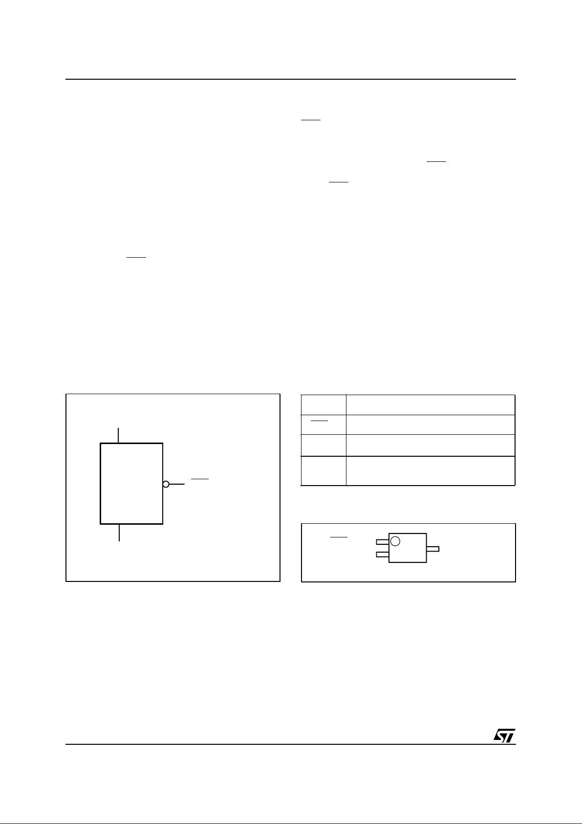
Table 2. Signal Names
V
SS
RST
RST
V
CC
Note: 1. For STM1812, STM1817
Ground
Active-low Reset Output
(1)
Active-high Reset Output
Supply Voltage and Input for Reset
Threshold Monitor
Figure 3. SOT23-3 Connections
RST (RST)
V
CC
Note: RST for STM1812 and STM1817
1
3
2
AI09649
V
SS
4/20
Figure 4. Hardware Hookup
V
CC
STM1810/1811/1812/1813/1815/1816/1817/1818
V
CC
STM181x
(1)
RST
Push-button
V
SS
Note: 1. RST for STM1812 and S TM1817 (see Ta bl e 1. , Device Opti ons)
2. Only valid for STM1813 and STM1818.
RESET
(2)
MCU
RESET
Input
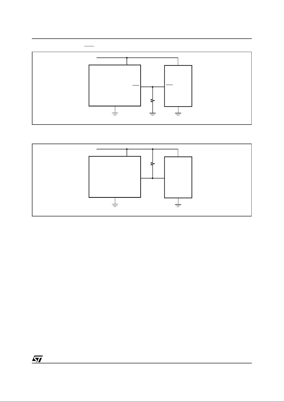
FUNCTI ONAL BLOCK DIAGRAMS
Figure 5. Push-pull Active-Low Output (STM1810/1812/ 181 5/18 17)
V
CC
V
RST
COMPARE
t
rec
Generator
V
CC
V
SS
AI09652a
(1)
RST
AI09651a
Note: 1. RST for STM 1812 and STM 1817.
Figure 6. Open Drain, Active-Low Output (STM1811/1816)
(1)
V
CC
Note: 1. 5.5kΩ inter n al pull- up resist or
t
V
RST
COMPARE
rec
Generator
5.5kΩ
RST
AI09672
Figure 7. Open Drain, Active-Low Output (Bi-directional, Manual Reset Detect, STM1813/1818)
(1)
5.5kΩ
RST
AI09673
V
CC
V
RST
Note: 1. 5.5kΩ inter n al pull- up resist or
COMPARE
t
rec
Generator
Push-button
Detect
5/20

STM1810/1811/1812/1813/1815/1816/1817/1818
PIN DES CRIPTIONS
See Figure 2., Logic Diagram and Table 2., Signal
Names for a brief overview of the signals connect-
ed to this de vice.
Active-Low RST
low when V
long as V
CC
mains low for t
Output (Push-pull). Pulses
drops below V
CC
, and stays low as
RST
is below the reset threshold. It re-
after VCC rises above the reset
rec
threshold.
Active-Low RST
low when V
long as V
CC
mains low for t
thres ho ld. R ST
Output (Open D rain) . Pulses
drops below V
CC
, and stays low as
RST
is below the reset threshold. It re-
after VCC rises above the reset
rec
output has a n internal 5.5k Ω p ull-
up resistor.
Table 3. STM1810/STM1815
Pin Name Function
1RST
2
3
V
V
Active-low Reset Output (Push-pull)
Supply Voltage and Input for Reset Threshold Monitor
CC
Ground
SS
Active-hi gh R S T Ou t put (P us h -p ul l ). Pulses
high when V
as long as V
mains high for t
threshold.
Active-Low RST
nal 5.5kΩ pull-up) with Manual Reset Detect.
Pulses low when V
is externally pulled low for at least 1.5µs. It remains low for t
set threshold, or after the external manual reset is
released (see Figure 10., page 8). RST
an internal 5.5kΩ pull-up resistor.
V
CC
tor.
V
SS
ply. It must be connected to the system ground.
drops below V
CC
is below the reset threshold. It re-
CC
after VCC rises above the reset
rec
, and stays high
RST
Output (Open Drain with inter-
drops below V
CC
after VCC rises above the re-
PBRST
RST
, or RST
output has
. Supply voltage and input for V
compara-
RST
. Ground, is the reference for the power sup-
Table 4. STM1811/STM1816
Pin Name Function
1RST
2
3
V
V
Active-low Reset Output (Open Drain, with internal 5.5kΩ pull-up resistor)
Supply Voltage and Input for Reset Threshold Monitor
CC
Ground
SS
Table 5. STM1812/STM1817
Pin Name Function
1 RST Active-high Reset Output (Push-pull)
2
3
V
V
Supply Voltage and Input for Reset Threshold Monitor
CC
Ground
SS
Table 6. STM1813/STM1818
Pin Name Function
1RST
2
3
V
V
Active-low Reset Output (Open Drain, with internal 5.5kΩ pull-up) with Push-Button/Manual
Reset Detect
Supply Voltage and Input for Reset Threshold Monitor
CC
Ground
SS
6/20

OPERATION
Reset Output
The STM181x asserts a reset signa l to t he M icrocontroller (MCU) whenever V
reset threshold (V
down to V
= 1.0V (0° to 105°C). A microcontrol-
CC
), and is guaranteed valid
RST
ler’s (MCU) reset input starts the MCU in a known
state. The STM1810 - STM1813/ STM1815 STM1818 Low Power Reset circuits assert reset to
prevent code-execution errors during power-up,
power-down, and brownout conditions (Figure
8., page 7).
During power-up, once V
threshold an internal timer keeps RST
reset time-out period, t
. After this interval, RST
rec
returns high.
If V
drops below the reset threshold, RST goes
CC
low. Each time RST
is asserted, it stays low for at
least the reset time-out period. Any time V
below the reset threshold, the internal timer clears.
The reset timer starts when V
reset threshold. Reset t
rec
externally initiated rising edge on the RST
(STM1813/STM1818), following a low signal of
1.5µs minimum duration.
Push-Button Detect Reset (STM1813/1818)
Many systems require push-button re set capabil ity
(Figure 9., page 8), allowing the user or external
logic circuitry to initiate reset. On the STM1813/
STM1818, a logic low on RST
1.5µs asserts a reset. RST
100ms minimum reset time-out delay (t
manual reset input shorter than 1.5µs may release
without the 1 00ms minimum reset time-out
RST
delay. To fac ilitate us e with mechanic al s witche s,
the STM1813/STM1818 contain internal debounce circuitry. A debounced waveform is shown
in Fi gur e 10. ,page 8 The RST
nal 5.5kΩ pull-up resistor.
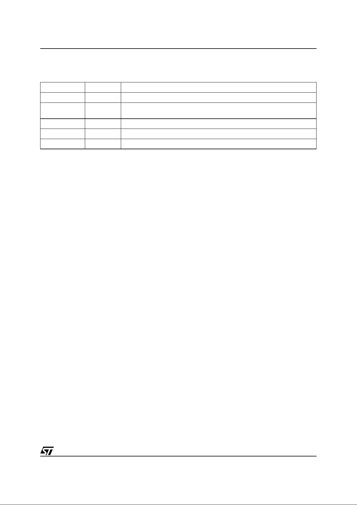
Interfacing to Bidirectional Microcontrollers
(MCU’s)
As the RST
output on the STM1811/STM1816 is
open drain, these devices interface easily with
MCU’s that have bidirectional reset pins. Connect-
goes below the
CC
exceeds the reset
CC
low for the
goes
CC
returns above the
CC
is also triggered by an
pin
held for greater than
deasserts following a
). A
rec
output has an inter-
STM1810/1811/1812/1813/1815/1816/1817/1818
ing the µP supervisor’s reset (RST
to the microcontroller’s reset (RST
ther device to asse rt reset (Figure 11., page 8). No
externa l pull-up resistor is require d, as it is w ithin
the STM1811/STM1816.
Negative Go in g V
Transients
CC
The STM181x are relatively immune to negativegoing V
transients (glitches). Figure
CC
20., page 13 shows typical transient duration ver-
sus reset comparator overdrive (for which the
STM181x will NOT generate a reset pulse). The
graph was gene rated using a negative pul se applied to V
starting at 0.5V above the actual re-
CC,
set threshold and ending below it by the
magnitude indicated (comparator ov erdrive). The
graph indicates the maximum pulse width a negative V
transient can ha ve without cau sing a re-
CC
set pulse. As the magnitude of the transient
increases (further below the thres hold), the maximum allowable pulse width decreases . Any combination of duration and overdrive which lies under
the curve will NOT generate a reset signal. Typically, a V
transient that goes 100mV below the
CC
reset threshold and lasts 20µs or less will not
cause a reset pulse. A 0.1µF bypass capacitor
mounted as close as possibl e to the V
vides additional transient immunity.
Valid R ST
When V
Output Down to VCC = 0V
falls below 1V, the RST output no long-
CC
er sinks current, but becomes an open circuit. In
most systems this is not a problem, as most MCUs
do not operate below 1V. However, in applications
where RST
output must be valid down to 0V, a
pull-down resistor may be added t o hold the RST
output low (see Figure 12., page 9). This resi stor
must be large enough to not load the RST
and still be small enough to pull the output to
ground. A 100kΩ res istor is recommended .
Note: The same situation applies for the activehigh RST of the STM1810/1812. A 100kΩ pul l-up
resistor to V
valid for V
should be used if RST must remain
CC
< 1.0V .
CC
) output directly
) pin allows ei-
pin pro-
CC
output,
Figure 8. Reset Timing Diagram
V
CC
V
RST
(1)
RST
Note: 1. RST for STM1812 and S TM1817
CC
(min)
V
RST
t
t
rec
rec
AI09653
7/20

STM1810/1811/1812/1813/1815/1816/1817/1818
Figure 9. Push-Button Manual Reset with MR Detect (STM1813/1818)
V
CC
STM1813
STM1818
V
CC
5.5kΩ
Reset
Monitor
V
SS
RST
Micro RESET
Push-button RESET
AI09654
Figure 10. Manual Reset Timing Diagram, Switch Bounce/Debou nce (STM1813/ 1818)
V
CC
(Open)
External
Push-button
tPBRST
Switch Bounce
(Closed)
RST
Figure 11. Interfacing MCUs with Bi-Directional Reset Pins (RST
V
CC
tPBRST
, Open Drain, STM1811/1816)
AI09655
STM1811
STM1816
V
CC
5.5kΩ
RST
V
SS
RST
Input
V
CC
MCU
V
SS
AI09656
8/20
STM1810/1811/1812/1813/1815/1816/1817/1818
Figure 12. Va lid R eset (RST) Output Down to VCC = 0V (Push-pull)
V
CC
STM1810
V
CC
V
STM1815
MCU
RST
V
SS
RST
Input
(1)
R
P
V
Note: 1. ~100 kΩ re sistor reco m m ended.
Figure 13. Vali d Re set (RST) Outp ut Down to VCC = 0V (Push-pull)
V
CC
STM1812
STM1817
V
CC
(1)
R
P
V
MCU
RST
RST
Input
V
SS
V
CC
SS
AI09657
CC
SS
Note: 1. ~100 kΩ re sistor reco m m ended.
AI09658
9/20

STM1810/1811/1812/1813/1815/1816/1817/1818
TYPICAL OPERATING CHARACTERISTICS
Note: Typical values are at TA = 25°C .
Figure 14. Supply Current vs. Temperature (no load )
5
4
3
2
Supply Current (µA)
1
VCC = 1.8V
VCC = 3V
VCC = 5V
0
–40 –20 0 20 40 60 80 100
Temperature (˚C)
Figure 15. Normalized Re set Time- o ut Period (t
1.07
1.05
)
rec
1.03
Period (t
1.01
Normalized Reset Time-out
0.99
–40 –20 0 20 40 60 80 100
Temperature (°C)
) vs. Temperature - VOD = VTH – VCC
rec
AI10403
AI10402
10/20

STM1810/1811/1812/1813/1815/1816/1817/1818
Figure 16. VCC-to-Reset Output Delay vs. Temperature - VOD = VTH – VCC
3.0
2.5
2.0
1.5
1.0
-to-Reset Output Delay (µs)
CC
V
0.5
0.0
–40 –20 0 20 40 60 80 100
Temperature (°C)
AI10404
Figure 17. Voltage Output Low vs. I
0.10
0.08
0.06
(V)
OUT
V
0.04
0.02
0.00
0123456
SINK
I
SINK
(mA)
VCC = 3V
AI10406
11/20

STM1810/1811/1812/1813/1815/1816/1817/1818
Figure 18. Voltage Output High vs. I
1.20
1.00
0.80
SOURCE
CC
/ V
0.60
OUT
V
0.40
0.20
0.00
0.0 1.0 2.0 3.0 4.0 5.0 6.0
I
SOURCE
(mA)
Figure 19. Nor m a liz ed R es et Threshol d vs . Tem perature
1.010
VCC = 3V
AI10407
1.005
1.000
0.995
Normalized Reset Threshold Voltage
0.990
–40 –20 0 20 40 60 80 100
Temperature (°C)
AI10405
12/20

STM1810/1811/1812/1813/1815/1816/1817/1818
Figure 20. Max Transient Duration NOT Causing Reset Pulse vs. Reset Threshold Overdrive
30
25
20
15
10
Transient Duration (µs)
5
0
10 100 1000
Reset Threshold Overdrive (mV)
Note: Reset occurs above the li ne.
AI10408
13/20

STM1810/1811/1812/1813/1815/1816/1817/1818
MAXIMUM RA T ING
Stressing the device above the rating l isted in the
Absolute Maximum Ratings” table may cause permanent damage to the device. These are stress
ratings only and operation of the device at t hese or
any other conditions ab ove those i ndicated in t he
Operating sections of this specificat ion is not im-
Table 7. Absolute Maximum Ratings
Symbol Parameter Value Unit
plied. Exposure to Absolute Maximum Rating conditions for extended periods may affect device
reliability. Refer also to the STMicroelectronics
SURE Program and other relevan t quality documents.
T
STG
(1)
T
SLD
V
IO
V
CC
I
O
P
D
Note: 1. Reflow at peak temperature of 2 55°C to 260° C f or < 30 seconds (total thermal budg et not to exce ed 180°C for between 90 t o 150
seconds).
Storage Temperature (VCC Off)
Lead Solder Temperature for 10 seconds 260 °C
Input or Output Voltage
Supply Voltage –0.3 to 7.0 V
Output Current 20 mA
Power Dissipation 320 mW
–55 to 150 °C
–0.3 to V
CC
+0.3
V
DC AND AC PARAMETERS
This section summarizes t he operating m easurement conditions, and the DC and AC characteristics of the device. The parameters in the D C and
AC characteristics Tables that follow, are derived
from tests performed under the Measurement
Table 8. Operating and AC Measurement Conditions
Parameter STM1810 - 1818 Unit
V
Supply Voltage
CC
Ambient Operating Temperature (T
Input Rise and Fall Times ≤ 5ns
Input Pulse Voltages
Input and Output Timing Ref. Voltages
)
A
Conditions summarized in Table 8, Operating and
AC Measurement Conditions. Designers should
check that the operating cond itions in their circuit
match the operating conditions when relying on
the quoted parameters.
1.0 to 5.5 V
–40 to 105 °C
0.2 to 0.8V
0.3 to 0.7V
CC
CC
V
V
Figure 21. AC Testing Input/Output Waveforms
0.8V
0.2V
14/20
CC
CC
0.7V
0.3V
AI02568
CC
CC

STM1810/1811/1812/1813/1815/1816/1817/1818
Table 9. DC and AC Characteristics
Sym
V
V
Alter-
native
CC
I
CC
V
IH
V
IL
OH
Operating Voltage
VCC Supply Current
Input High Voltage STM1813/1818 only
Input Low Voltage STM1813/1818 only
Output High Voltage 0 < IOH < 500µA
RST Output Source Current
I
OH
RST Output Source Current
Description
Test Condition
T
= 0 to +105°C
A
= –40 to +105°C
T
A
= 3.6V, No load
V
CC
= 5.5V, No load
V
CC
≥ V
V
CC
(max), Reset not
RST
asserted (STM1810/STM1815)
V
≤ V
CC
(min), Reset asserted
RST
(STM1812/STM1817)
VCC ≥ 2.7V, Reset asserted,
C
I
OL
OUT
RST Output Sink Current
RST Output Sink Current
Output Capacitance
(2)
V
= 0.4V (STM1810/1811/
OUT
1813/1815/1816/1818)
V
≥ 2.7V, Reset not asserted,
CC
V
= 0.4V, (STM1812/1817)
OUT
Reset Thresholds
STM181xL
STM181xM
V
RST
Reset Threshold
STM181xT
STM181xS
STM181xR
V
= (VTH + 100mV) falling to
t
RD
t
rec
VCC to RST Delay
RST Pulse Width
CC
(VTH – 200mV)
V
CC
Rising
Push-Button Reset Detect (STM1813, STM1818)
t
PB
t
PBRST
Note: 1. Valid for A m bi ent Operat in g T em perature: TA = –40 to 105°C; VCC = 1.2V to 5.5V (except where noted).
2. T he STM1811/1813/1816/1818 have an internal pul l -up resist or which may si nk 1mA of current.
Push-button Detect to RST STM1813/1818 1.5 µs
Push-button RST Time-out From Rising Edge
Internal Pull-up Resistance
STM1811/1816 3.5 5.5 7.5 kΩ
STM1813/1818 3.1 5.5 7.5 kΩ
(1)
Min Typ Max Unit
1.0 5.5 V
1.2 5.5 V
0.7V
CC
V
–
CC
0.5
10 mA
10 mA
25°C 4.62 V
–40 to 105°C 4.50 4.75 V
25°C 4.37 V
–40 to 105°C 4.25 4.49 V
25°C 3.06 V
–40 to 105°C 2.98 3.15 V
25°C 2.88 V
–40 to 105°C 2.80 2.97 V
25°C 2.55 V
–40 to 105°C 2.47 2.64 V
100 150 200 ms
100 150 200
410µA
916µA
V
0.4
VCC
– 0.1
V
V
350 µA
350 µA
10 pF
25µs
ms
15/20

STM1810/1811/1812/1813/1815/1816/1817/1818
PACKAG E MECHANICAL
Figure 22. SOT23-3 – 3-lead Small Outline Transistor Package Outline
E
E1
B
1
e1
0.15
e
M
D
CAB
A1
0.20 C A B
3X b
C
M
A
θ
C
L1
3X
0.10 C
C
A2
L
SOT23-3
Note: Drawing is not to scale.
Table 10. SOT23-3 – 3-lead Small Outline Transistor Package Mechanical Data
Symbol
Typ Min Max Typ Min Max
A 0.89 1.12 0.035 0.044
A1 0.01 0.10 0.001 0.004
A2 0.88 1.02 0.035 0.042
b 0.30 0.50 0.012 0.020
C 0.08 0.20 0.003 0.008
D 2.80 3.04 0.110 0.120
mm inches
A
E 2.10 2.64 0.083 0.104
E1 1.20 1.40 0.047 0.055
e 0.89 1.03 0.035 0.041
e1 1.78 2.05 0.070 0.081
L 0.54 0.021
L1 0.40 0.60 0.016 0.024
Θ 0° 8° 0° 8°
N3 3
16/20

STM1810/1811/1812/1813/1815/1816/1817/1818
PART NUMBERING
Table 11. Ordering Information Scheme
Example: STM1810 L WX 7 F
Device Type
STM181x
Reset Threshold Voltage
STM1810 - 1813:
L = V
M = V
STM1815 - 1818:
T = V
S = V
R = V
= 4.50V to 4.75V (4.62 typ)
RST
= 4.25V to 4.49V (4.37 typ)
RST
= 2.98V to 3.15V (3.06 typ)
RST
= 2.80V to 2.97V (2.88 typ)
RST
= 2.47V to 2.64V (2.55 typ)
RST
Package
WX = SOT23-3
Temperature Range
7 = –40 to 105°C
Shipping Method
F = Pb-Free Package, Tape & Reel
Note: 1. Contact the local ST sales office for availability.
For other options, or for more information on any aspect of this device, please contact the ST Sales Office
nearest you.
17/20

STM1810/1811/1812/1813/1815/1816/1817/1818
Table 12. Marking Description
Part Number Reset Threshold Output Topside Marking
STM1810L 4.62V Push -Pull R ST
STM1810M 4.37V Push -Pull R ST
STM1811L 4.62V Open Drain RST
STM1811M 4.37V Open Drain RST
STM1812L 4.62V Push-Pull RST
STM1812M 4.37V Push-Pull RST
STM1813L 4.62V Open Drain RST
STM1813M 4.37V Open Drain RST
STM1815T 3.06V Push-Pull R ST
STM1815S 2.88V Push-Pull RST
STM1815R 2.5 5V Push-Pull RST
STM1816T 3.06V Open Drain RST
STM1816S 2.88V Open Drain RST
STM1816R 2.55V Open Drain RST
STM1817T 3.06V Push-Pull RST
STM1817S 2.88V Push-Pull RST
STM1817R 2.55V Push-Pull RST
STM1818T 3.06V Open Drain RST
STM1818S 2.88V Open Drain RST
STM1818R 2.55V Open Drain RST
18/20
STM1810/1811/1812/1813/1815/1816/1817/1818
REVISION HISTORY
Table 13. Document Revision History
Date Revision Revision Details
26-Aug-04 1.0 First Issue
05-Oct-04 2.0
19-Nov-04 3.0 Update dimensions (Table 10)
07-Dec-04 4.0 Remove some voltage options (Table 1, 9, 11, 12)
29-Jun-05 5 Temperature range change (Figure 14, 15, 16, 19; Table 8, 9, 11)
Update reset characteristics, add typical graphs, remove SC70 references (Figure
1, 2, 4, 7, 11, 12, 13, 14, 15, 16, 17, 18, 19, 20; Table 9, 11, 12)
19/20

STM1810/1811/1812/1813/1815/1816/1817/1818
Information furnished is believed to be accurate and reliable. However, STMicroelectronics a ssumes no responsibility fo r the c onsequences
of use of such information nor for any infringement of patents or other rights of third parties which may result from its use. No license is granted
by implication or otherwise under any patent or patent rights of STMicroelectronics. Specifications mentioned in this publication are subject
to change without notice. This publication supersedes and replaces all information previously supplied. STMicroelectronics products are not
authori zed for use as crit i cal compon ents in life support devic es or systems w i thout express written approval of STMicroele ct ronics.
The ST logo is a registered trademark o f STM i croelectronics.
All other nam es are the pro perty of their respective owners
© 2005 STMi croelectro ni cs - All righ ts reserved
Australi a - Belgium - B razil - Canad a - China - Cze ch Republic - F i nl and - Franc e - Germany - Hong Kong - Ind ia - Is rael - Italy - Japan -
Malaysia - M al ta - Morocco - Singapore - Spain - Swe den - Switzerland - Uni ted Kingdom - United Sta tes of Americ a
STMicroelectron ics group of com panies
www.st.com
20/20
 Loading...