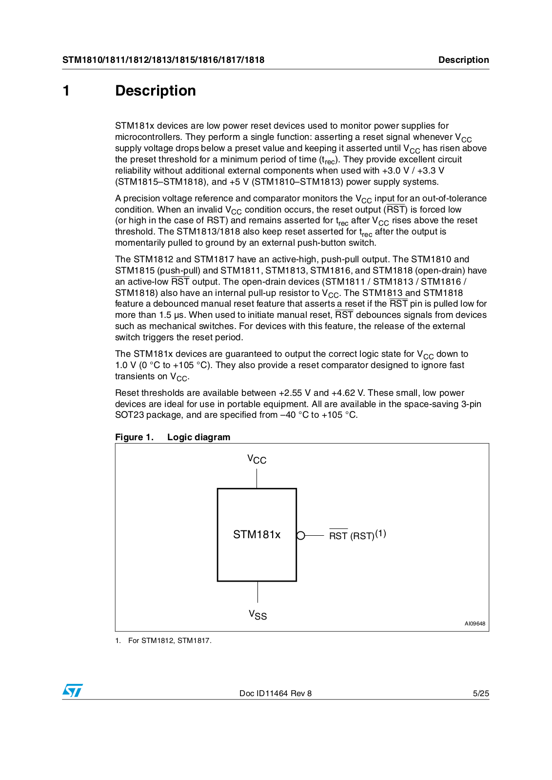
How it Works
Log In / Sign Up
Buy Points
How it Works
FAQ
Contact Us
Questions and Suggestions
Users
ST
Loading...
S
STiH251
STiH273
STiH416
STL8NH3LL
STLA01
STLA02
STLC1510
STLC2150
STLC2410B
STLC3055N
STLC3075
STLC3080
STLC5046
STLD41
STLED25
STLED316S
STLED325
STLink
STLINK-V3SET
STLM20
STLM75
STLQ015XG25R
STLQ015XG28R
STLQ015XG30R
STLQ015XG31R
STLQ015XG33R
STLQ50C18R
STLQ50C25R
STLQ50C33R
STLQ50C50R
STLQ50C-R
STLQ50M18R
STLQ50M25R
STLQ50M33R
STLQ50M50R
STLQ50M-R
STLVD111
STLVDS31B
STM1001
STM1061
STM1403
2
STM1404
STM1645-30
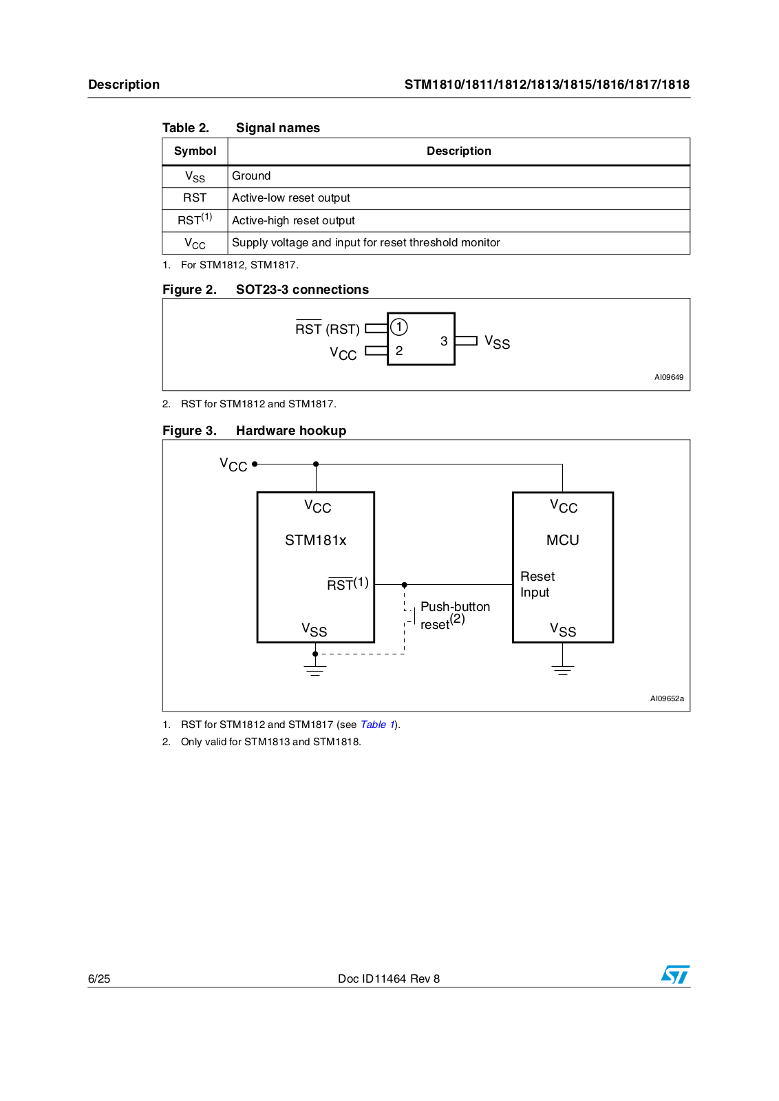
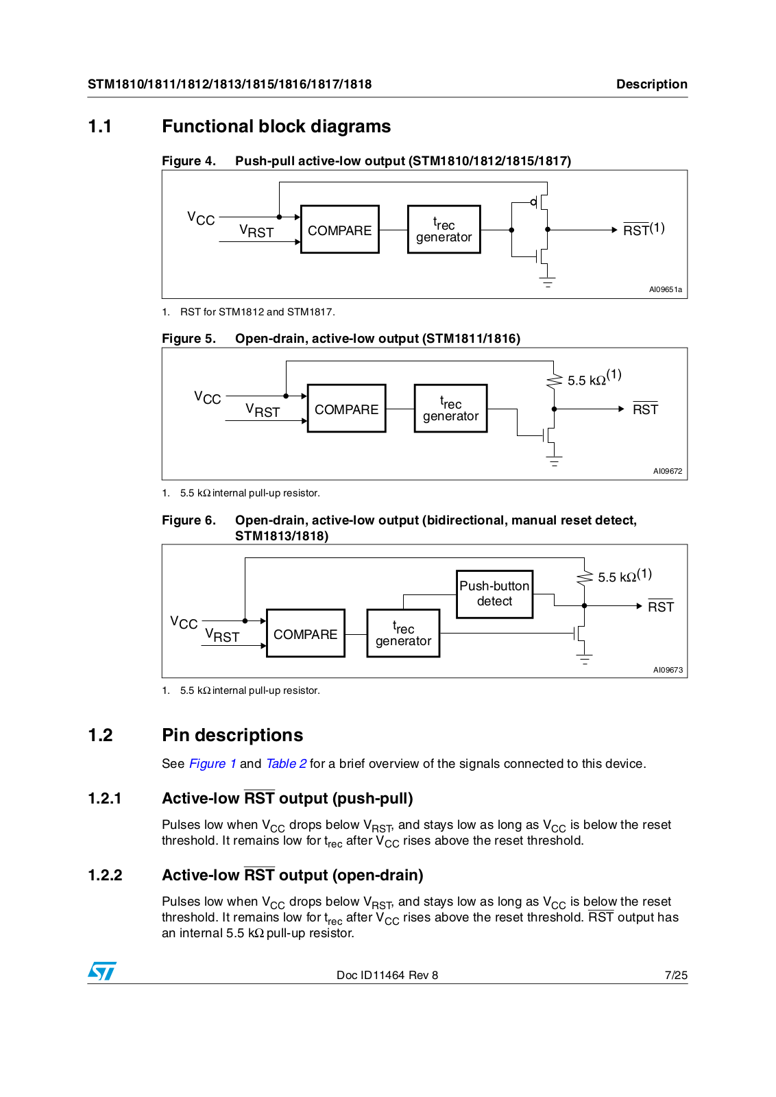
STM1810
STM1811
STM1812
STM1813
STM1815
STM1816
STM1817
STM1818
2
STM1831
STM2DPFS30L
STM32
12
STM320518-EVAL
STM32091C-EVAL
STM32100B
2
STM3210B
STM3210B-EVAL
STM3210B-MCKIT
STM3210B-PFSTICK
STM3210C
STM3210C-SK-IAR
STM3210C-SK-KEI
STM3210E
STM3210E-EVAL
2
STM3210E-SK-IAR
STM3210E-SK-KEI
STM3220F-EVAL
STM3220G
STM3220G-EVAL
2
STM3221G-EVAL
2
STM32303C-EVAL
2
STM32373C-EVAL
STM3240G
STM3240G-EVAL
3
STM3240G-SK-IAR
STM3240G-SK-KEI
STM3241G-EVAL
STM32479I-EVAL
STM32746G-EVAL
STM32756G-EVAL
STM32CMICTCP-BK
STM32Cube
2
STM32CubeF2
STM32CubeH7
STM32F0
STM32F030
STM32F051C4
STM32F051C6
STM32F051C8
STM32F051K4
STM32F051K6
STM32F051K8
STM32F0 Series
STM32 Nucleo
STM32 Nucleo-32
STM32 Nucleo-64
STM32 ODE
STM-STUDIO
Loading...
Loading...
Nothing found
STM1817
User Manual
25 pgs
326.74 Kb
0
Table of contents
Loading...
ST STM1810, STM1811, STM1812, STM1813, STM1815 User Manual
...
ST STM1810, STM1811, STM1812, STM1813, STM1815, STM1816, STM1817, STM1818 User Manual
Download
Specifications and Main Features
Frequently Asked Questions
User Manual
Download
Loading...
+
17
hidden pages
Unhide
You need points to download manuals.
1 point = 1 manual.
You can buy points or you can get point for every manual you upload.
Buy points
Upload your manuals