

Datasheet STLQ015XG25R, STLQ015XG28R, STLQ015XG30R, STLQ015XG31R, STLQ015XG33R Datasheet (ST)
Features
■ Input voltage from 1.5 to 5.5 V
■ Very low quiescent current:
– 1.0 µA (typ) at no load
– 1.4 µA (typ) at 150 mA load
– 1 nA (typ) in OFF mode
– 200 nA max in OFF mode at 125 °C
■ Output voltage tolerance: ± 2% at 25 °C
■ 150 mA guaranteed output current
■ Wide range of output voltages: 0.8 V to 3.3 V in
100 mV steps
■ Logic-controlled electronic shutdown
■ Compatible with ceramic capacitor (C
µF)
■ Internal current and thermal limit
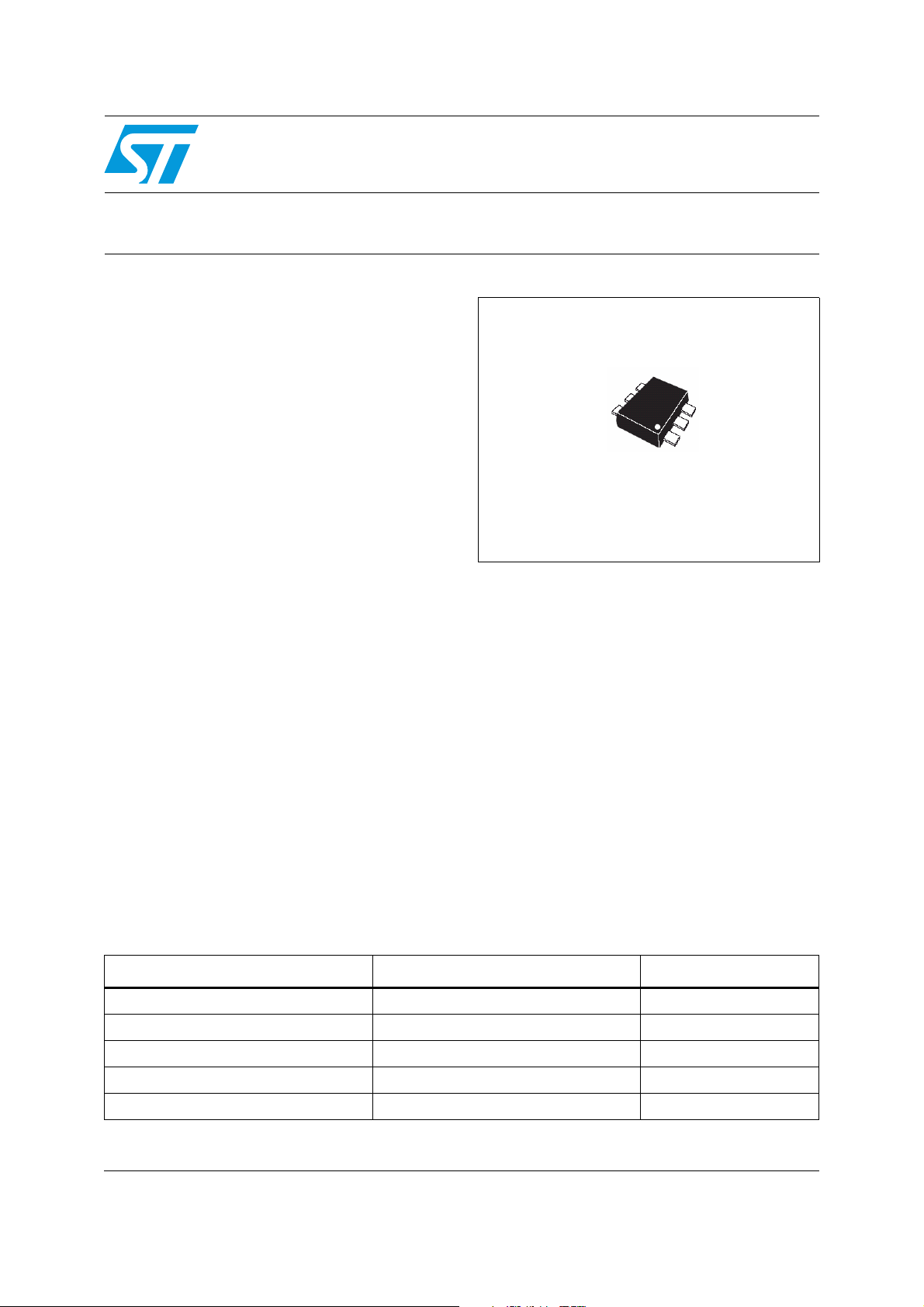
■ Package: SOT666-6L
■ Temperature range: -40 °C to 125 °C
OUT
= 1
STLQ015xx
150 mA, ultra-low quiescent current
linear voltage regulator
SOT666
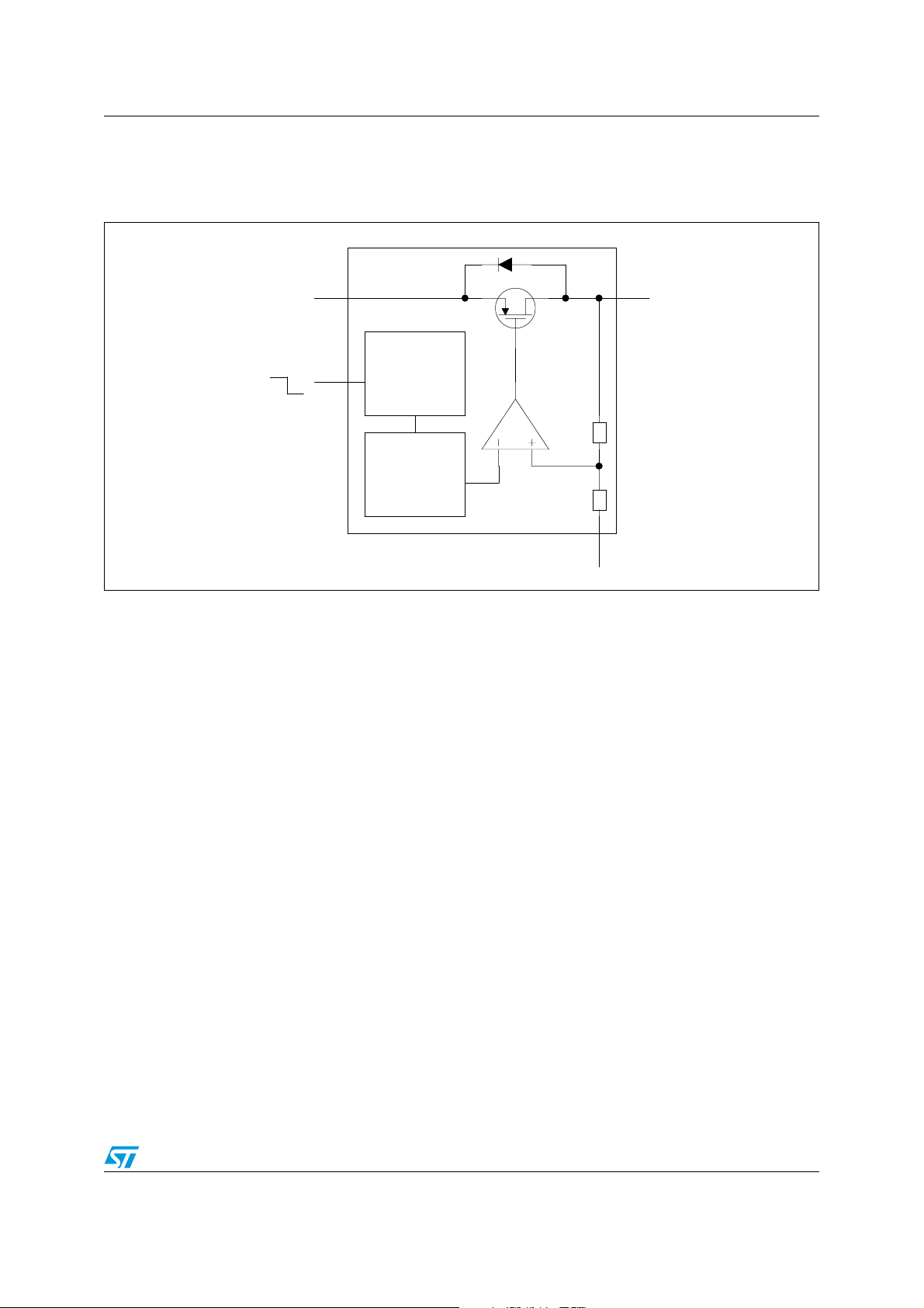
requiring very long standby time. The enable logic
control function puts the STLQ015xx in shutdown
mode, reducing total current consumption to 1 nA.
The device also includes short-circuit constantcurrent limiting and thermal protection. Typical
applications for the device are portable and
battery-powered systems, electronic sensors, and
microcontroller power supply.
Description
The STLQ015xx provides 150 mA of maximum
current from an input voltage ranging from 1.5 V
to 5.5 V, with a typical dropout voltage of 112 mV.
The key feature of this device is its quiescent
current, which is just 1.4 µA at maximum output
current. The device is stable with a ceramic
capacitor on the output. It offers very low
quiescent current, extending battery life and
making the device suitable for applications
Table 1. Device summary
Part numbers Order codes Output voltages
STLQ015XX25 STLQ015XG25R 2.5 V
January 2011 Doc ID 17285 Rev 2 1/17
STLQ015XX28 STLQ015XG28R 2.8 V
STLQ015XX30 STLQ015XG30R 3.0 V
STLQ015XX31 STLQ015XG31R 3.1 V
STLQ015XX33 STLQ015XG33R 3.3 V
www.st.com
17

Contents STLQ015xx
Contents
1 STLQ015xx block diagram . . . . . . . . . . . . . . . . . . . . . . . . . . . . . . . . . . . . 3
2 Pin configuration and description . . . . . . . . . . . . . . . . . . . . . . . . . . . . . . 4
3 Typical application . . . . . . . . . . . . . . . . . . . . . . . . . . . . . . . . . . . . . . . . . . 5
4 Maximum ratings . . . . . . . . . . . . . . . . . . . . . . . . . . . . . . . . . . . . . . . . . . . . 6
5 Electrical characteristics . . . . . . . . . . . . . . . . . . . . . . . . . . . . . . . . . . . . . 7
6 Typical performance characteristics . . . . . . . . . . . . . . . . . . . . . . . . . . . . 9
7 Package mechanical data . . . . . . . . . . . . . . . . . . . . . . . . . . . . . . . . . . . . 12
8 Different output voltage versions of the STLQ015xx
available on request . . . . . . . . . . . . . . . . . . . . . . . . . . . . . . . . . . . . . . . . 15
9 Revision history . . . . . . . . . . . . . . . . . . . . . . . . . . . . . . . . . . . . . . . . . . . 16
2/17 Doc ID 17285 Rev 2
STLQ015xx STLQ015xx block diagram
1 STLQ015xx block diagram
Figure 1. Device block diagram
OUTIN
OUTIN
ENABLE
ENABLE
ON
ON
OFF
OFF
EN
EN
Thermal Prot.
Thermal Prot.
Over Current
Over Current
Vreference
Vreference
R1
R1
R2
R2
GND
GND
Doc ID 17285 Rev 2 3/17
Pin configuration and description STLQ015xx
2 Pin configuration and description
Figure 2. Pin configuration (top view)
Table 2. Pin description
Pin Symbol Function
Enable input.
1EN
2 GND Ground
3 IN Input voltage
Set V
Set V
= High to turn on the device.
EN
= Low to turn off the device.
EN
4 OUT Output voltage
5 NC Not connected
6 NC Not connected
4/17 Doc ID 17285 Rev 2
STLQ015xx Typical application
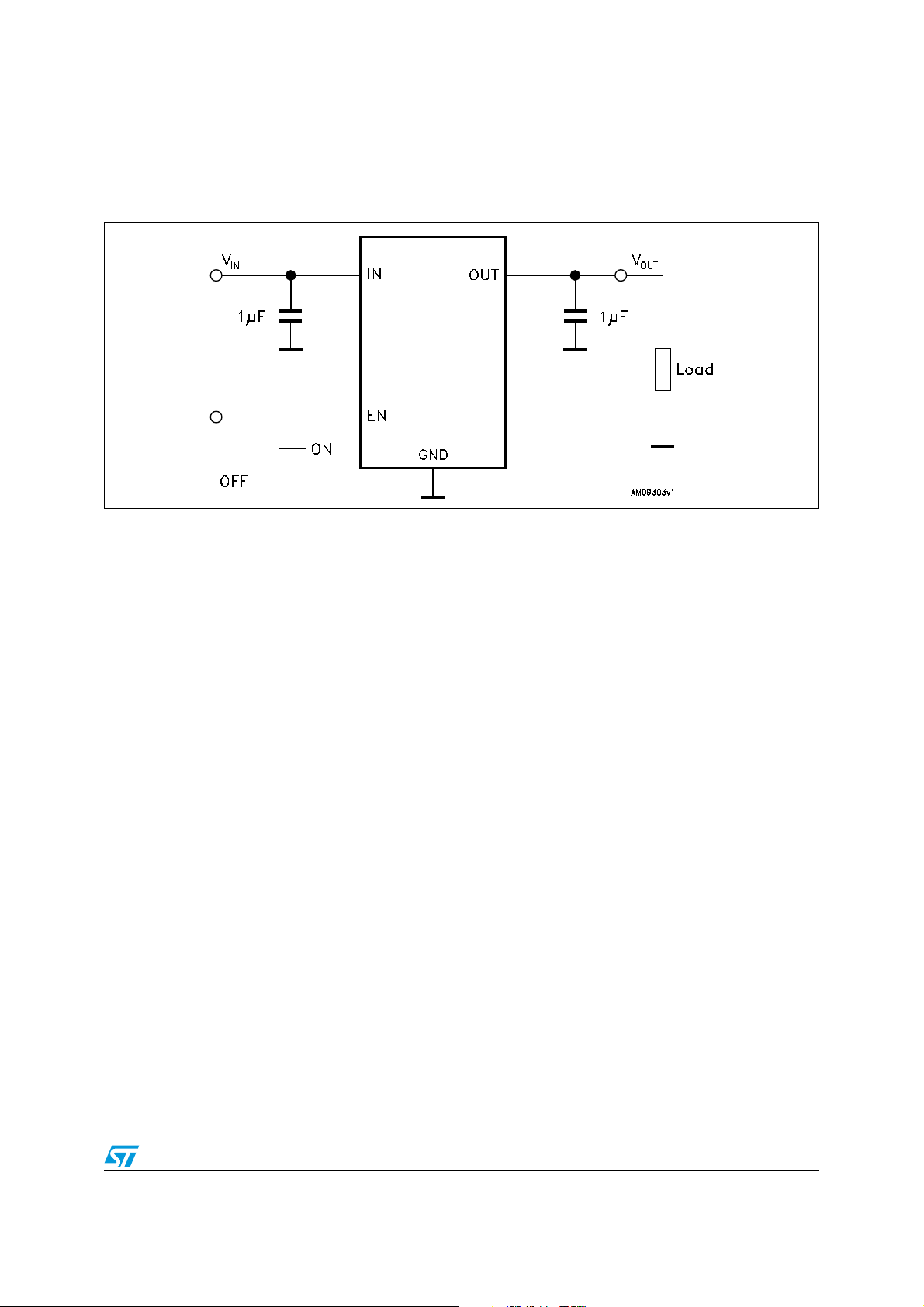
3 Typical application
Figure 3. Typical application circuit
Doc ID 17285 Rev 2 5/17
Maximum ratings STLQ015xx
4 Maximum ratings
Table 3. Absolute maximum ratings
Symbol Parameter Value Unit
V
V
I
V
IN
OUT
EN
OUT
DC input voltage -0.3 to 7 V
DC output voltage - 0.3 to VIN + 0.3 V
Enable input voltage - 0.3 to VIN + 0.3 V
Output current Internally limited mA
Human Body Model ±
3kV
ESD
Machine Model ± 300 V
T
P
STG
T
D
OP
Power dissipation Internally limited mW
Storage temperature range -65 to 150 °C
Max junction temperature 150 °C
Note: Absolute maximum ratings are those values beyond which damage to the device may occur.
Functional operation under these conditions is not implied. All values are referred to GND.
Table 4. Thermal data
Symbol Parameter SOT666 Unit
R
R
thJA
thJC
Thermal resistance junction-ambient 132 °C/W
Thermal resistance junction-case 56 °C/W
6/17 Doc ID 17285 Rev 2

STLQ015xx Electrical characteristics
5 Electrical characteristics
TJ = 25 °C, V
IN
= V
OUT(NOM)
+ 1 V, CIN = C
OUT
= 1 µF, I
= 1 mA, VEN = VIN, unless
OUT
otherwise specified.
Table 5. Electrical characteristics
Symbol Parameter Test conditions Min. Typ. Max. Unit
V
IN
V
OUTVOUT
ΔV
OUT-
LINE
ΔV
OUT-
LOAD
V
DROP
e
N
SVR
I
Q
I
OFF
I
SC
V
EN
I
T
T
SHDN
EN
ON
I
= 0 1.5 5.5
Operating input voltage
accuracy
Static line regulation V
Static load regulation I
Dropout voltage
(1)
Output noise voltage
Supply voltage rejection
= 0.8V
V
OUT
Quiescent current
Shutdown current
(2)
OUT
-40°C < T
I
OUT
I
OUT
I
OUT
OUT
OUT
I
OUT
I
OUT
< 125°C, I
J
= 1mA -2 2 %
= 1mA, V
OUT
= 1mA, -40°C < TJ < 125°C -3 3 %
+1V ≤ VIN ≤ 5.5V, I
= 1mA to 150mA ±0.002 %/mA
= 150mA 112
= 150mA, -40°C < TJ < 125°C 300
10kHz to 100kHz, I
V
= 0.8V
OUT
V
= V
IN
OUTNOM
V
I
V
V
I
V
V
I
I
I
= 0.1V, Freq. = 1kHz
RIPPLE
= 10mA
OUT
= V
IN
OUTNOM
= 0.1V, Freq.=10kHz
RIPPLE
= 1mA
OUT
= V
IN
OUTNOM
= 0.1V, Freq.=100kHz
RIPPLE
= 1mA
OUT
= 0 1.0 1.7
OUT
= 0 to 150mA,
OUT
-40°C < T
< 125°C
J
+ 1V +/-V
+ 1V +/-V
+ 1V +/-V
VIN input current in OFF mode:
V
= GND, -40°C < TJ < 125°C
EN
= 150mA 1.55 5.5
OUT
< 1V -20 +20 mV
= 1mA ±0.01 %/V
OUT
= 10mA,
OUT
RIPPLE
75 µV
40
RIPPLE
30
RIPPLE
15
1.7 2.4
1 200 nA
Short circuit current RL = 0 250 350 mA
Enable input logic low V
Enable input logic high V
Enable pin input current V
Turn-on time
(3)
= 1.5V to 5.5V 0.4 V
IN
= 1.5V to 5.5V 0.7 V
IN
= 5.5V 1 200 nA
EN
V
OUT
= 0.8 V, I
= 150 mA 160 µs
OUT
Thermal shutdown 170
Hysteresis 180
V
mV
RMS
dB
µA
°C
Doc ID 17285 Rev 2 7/17

Electrical characteristics STLQ015xx
Table 5. Electrical characteristics (continued)
Symbol Parameter Test conditions Min. Typ. Max. Unit
Capacitance (see typical
C
OUT
ESR 0.056 6 Ω
1. Dropout voltage is the input-to-output voltage difference at which the output voltage is 100 mV below its nominal value. This
specification does not apply for output voltages below 1.5 V
2. During shutdown and at no load, P-channel leakage current flowing through the internal resistor divider determines the
Output capacitor
increase of V
3. Turn-on time is the time measured between the enable input just exceeding V
reaching 95% of its nominal value
OUT
performance characteristics for
stability)
0.47 10 µF
high value and the output voltage just
EN
8/17 Doc ID 17285 Rev 2

STLQ015xx Typical performance characteristics
6 Typical performance characteristics
Figure 4. Output voltage vs. temperature Figure 5. Output voltage vs. input voltage
1.00%
1.00%
0.80%
0.80%
0.60%
0.60%
0.40%
0.40%
0.20%
0.20%
0.00%
0.00%
variation [%]
variation [%]
-0.20%
-0.20%
OUT
OUT
V
V
-0.40%
-0.40%
-0.60%
-0.60%
-0.80%
-0.80%
-1.00%
-1.00%
-40 -20 0 20 40 60 80 100 120 140
-40 -20 0 20 40 60 80 100 120 140
Figure 6. Output voltage vs. input voltage Figure 7. Dropout voltage vs. temperature
3.6
3.6
3.2
3.2
2.8
2.8
2.4
2.4
2.0
2.0
[V]
[V]
OUT
OUT
1.6
1.6
V
V
1.2
1.2
0.8
0.8
0.4
0.4
0.0
0.0
0.0 0.5 1.0 1.5 2.0 2.5 3.0 3.5 4.0 4.5 5.0 5.5
0.0 0.5 1.0 1.5 2.0 2.5 3.0 3.5 4.0 4.5 5.0 5.5
I
= 1 mA
I
= 1 mA
OUT
OUT
Temperature [°C]
Temperature [°C]
I
= 150 mA, V
I
= 150 mA, V
OUT
OUT
V
V
[V]
[V]
IN
IN
T= -40°C
T= -40°C
T= +25°C
T= +25°C
T= 125°C
T= 125°C
= 3.3 V
= 3.3 V
OUT
OUT
1.0
1.0
0.8
0.8
0.6
0.6
[V]
[V]
OUT
OUT
V
V
0.4
0.4
0.2
0.2
0.0
0.0
0.3 0.5 0.7 0.9 1.1 1.3 1.5 1.7 1.9
0.3 0.5 0.7 0.9 1.1 1.3 1.5 1.7 1.9
0.30
0.30
0.25
0.25
0.20
0.20
Vdrop [V]
Vdrop [V]
0.15
0.15
0.10
0.10
0.05
0.05
-40 -20 0 20 40 60 80 100 120 140
-40 -20 0 20 40 60 80 100 120 140
T= -40°C
T= -40°C
T= +25°C
T= +25°C
T= 125°C
T= 125°C
VO = 1.5 V
VO = 1.5 V
VO = 3.3 V
VO = 3.3 V
Temperature [°C]
Temperature [°C]
V
V
IN
IN
I
= 150 mA, V
I
= 150 mA, V
OUT
OUT
[V]
[V]
I
I
OUT
OUT
= 150 mA
= 150 mA
OUT
OUT
= 0.8 V
= 0.8 V
Figure 8. Dropout voltage vs. output current Figure 9. Quiescent current vs. temperature
0.30
0.30
VO = 1.5 V
0.25
0.25
0.20
0.20
0.15
0.15
Vdrop [V]
Vdrop [V]
0.10
0.10
0.05
0.05
0.00
0.00
0 0.05 0.1 0.15 0.2
0 0.05 0.1 0.15 0.2
VO = 1.5 V
VO = 3.3 V
VO = 3.3 V
[A]
[A]
I
I
OUT
OUT
2.00
2.00
V
= 1.5 V, VO = 0.8 V
V
= 1.5 V, VO = 0.8 V
IN
1.80
1.80
1.60
1.60
1.40
1.40
1.20
1.20
1.00
1.00
Iq [µA]
Iq [µA]
0.80
0.80
0.60
0.60
0.40
0.40
0.20
0.20
0.00
0.00
-40 -20 0 20 40 60 80 100 120 140
-40 -20 0 20 40 60 80 100 120 140
IN
V
= 4.3 V, VO = 3.3 V
V
= 4.3 V, VO = 3.3 V
IN
IN
Temperature [°C]
Temperature [°C]
IO = 0 mA
IO = 0 mA
Doc ID 17285 Rev 2 9/17

Typical performance characteristics STLQ015xx
Figure 10. Supply voltage rejection vs.
70
60
50
40
30
Supply Volt age reject ion [dB]
20
10
frequency
Vout=0.8V
Vout=3.3V
100 1000 100 00 100000
f [Hz]
Figure 11. Supply voltage rejection vs. I
50
50
40
40
30
30
20
20
10
10
Supply Voltage Rejection [db]
Supply Voltage Rejection [db]
V
= 1.5, VO = 0.8 V
V
= 1.5, VO = 0.8 V
IN
IN
V
= 4.3 V, VO = 3.3 V
V
= 4.3 V, VO = 3.3 V
IN
IN
0
0
0 20 40 60 80 100 120 140 160
0 20 40 60 80 100 120 140 160
[mA]
[mA]
I
I
OUT
OUT
f = 1 kHz
f = 1 kHz
Figure 12. Quiescent current vs. input voltage Figure 13. Quiescent current vs. output
2.40
2.40
2.20
2.20
2.00
2.00
1.80
1.80
1.60
1.60
1.40
1.40
1.20
1.20
Iq [µA]
Iq [µA]
1.00
1.00
0.80
0.80
0.60
0.60
0.40
0.40
0.20
0.20
0.00
0.00
0.0 0.5 1.0 1.5 2.0 2.5 3.0 3.5 4.0 4.5 5.0 5.5
0.0 0.5 1.0 1.5 2.0 2.5 3.0 3.5 4.0 4.5 5.0 5.5
VO = 0.8 V
VO = 0.8 V
VO = 3.3 V
VO = 3.3 V
IO = 1 mA
IO = 1 mA
[V]
[V]
V
V
IN
IN
Iq [µA]
Iq [µA]
current
2.00
2.00
1.80
1.80
1.60
1.60
1.40
1.40
1.20
1.20
1.00
1.00
0.80
0.80
0.60
0.60
0.40
0.40
0.20
0.20
0.00
0.00
0 20 40 60 80 100 120 140 160
0 20 40 60 80 100 120 140 160
VIN= 4.3 V, VO= 3.3 V
VIN= 4.3 V, VO= 3.3 V
VIN= 1.5 V, VO= 0.8 V
VIN= 1.5 V, VO= 0.8 V
TJ= 25 °C
TJ= 25 °C
I
I
[mA]
[mA]
OUT
OUT
OUT
Figure 14. Output noise voltage vs. frequency Figure 15. C
18.0
16.0
14.0
12.0
10.0
8.0
eN [uV/SQRT(Hz)]
6.0
4.0
2.0
0.0
10 100 1000 10000 100000
f [Hz]
3V3 Iload= 10mA
0V8 Iload= 10mA
10/17 Doc ID 17285 Rev 2
stability region
OUT
8.00
8.00
7.00
7.00
6.00
6.00
5.00
5.00
ESR MAX
4.00
4.00
3.00
3.00
ESR at 100 kHz [ohm]
ESR at 100 kHz [ohm]
2.00
2.00
1.00
1.00
0.00
0.00
0.0 1.0 2.0 3.0 4.0 5.0 6.0 7.0 8.0 9.0 10.0
0.0 1.0 2.0 3.0 4.0 5.0 6.0 7.0 8.0 9.0 10.0
ESR MAX
ESR MIN
ESR MIN
C
C
OUT
OUT
[µF]
[µF]

STLQ015xx Typical performance characteristics
Figure 16. Startup transient Figure 17. Enable transient
V
V
IN
IN
V
V
OUT
OUT
VIN from 0 to 1.5 V, VEN tied to VIN, No Load C
OUT
= 1 µF
V
V
EN
EN
V
V
OUT
OUT
V
= 1.5 V; VEN from 0 to 2 V, No Load, T = 25 °C
IN
Doc ID 17285 Rev 2 11/17

Package mechanical data STLQ015xx
7 Package mechanical data
In order to meet environmental requirements, ST offers these devices in different grades of
ECOPACK
specifications, grade definitions and product status are available at: www.st.com.
ECOPACK
®
packages, depending on their level of environmental compliance. ECOPACK®
®
is an ST trademark.
Table 6. SOT666 mechanical data
mm. inch.
Dim.
Min. Typ. Max. Min. Typ. Max.
A 0.45 0.60 0.018 0.024
A3 0.08 0.18 0.005 0.007
b 0.17 0.34 0.007 0.013
b1 0.19 0.27 0.34 0.007 0.011 0.013
D 1.50 1.70 0.059 0.067
E 1.50 1.70 0.059 0.067
E1 1.10 1.30 0.043 0.051
e0.50 0.020
L1 0.19 0.007
L2 0.10 0.30 0.004 0.012
L3 0.10 0.004
12/17 Doc ID 17285 Rev 2

STLQ015xx Package mechanical data
Figure 18. Drawing dimension SOT666
7366479
Doc ID 17285 Rev 2 13/17

Package mechanical data STLQ015xx
Figure 19. SOT666 footprint recommended data (mm.)
AM09302v1
14/17 Doc ID 17285 Rev 2

STLQ015xx Different output voltage versions of the STLQ015xx available on request
8 Different output voltage versions of the STLQ015xx
available on request
Table 7. Options available on request
Order codes Output voltages
STLQ015XG12R 1.2 V
STLQ015XG18R 1.8 V
Doc ID 17285 Rev 2 15/17

Revision history STLQ015xx
9 Revision history
Table 8. Document revision history
Date Revision Changes
23-Mar-2010 1 Initial release.
20-Jan-2011 2
Modified Table 6 on page 12 and Figure 18 on page 13.
Added Figure 19 on page 14.
16/17 Doc ID 17285 Rev 2

STLQ015xx
Please Read Carefully:
Information in this document is provided solely in connection with ST products. STMicroelectronics NV and its subsidiaries (“ST”) reserve the
right to make changes, corrections, modifications or improvements, to this document, and the products and services described herein at any
time, without notice.
All ST products are sold pursuant to ST’s terms and conditions of sale.
Purchasers are solely responsible for the choice, selection and use of the ST products and services described herein, and ST assumes no
liability whatsoever relating to the choice, selection or use of the ST products and services described herein.
No license, express or implied, by estoppel or otherwise, to any intellectual property rights is granted under this document. If any part of this
document refers to any third party products or services it shall not be deemed a license grant by ST for the use of such third party products
or services, or any intellectual property contained therein or considered as a warranty covering the use in any manner whatsoever of such
third party products or services or any intellectual property contained therein.
UNLESS OTHERWISE SET FORTH IN ST’S TERMS AND CONDITIONS OF SALE ST DISCLAIMS ANY EXPRESS OR IMPLIED
WARRANTY WITH RESPECT TO THE USE AND/OR SALE OF ST PRODUCTS INCLUDING WITHOUT LIMITATION IMPLIED
WARRANTIES OF MERCHANTABILITY, FITNESS FOR A PARTICULAR PURPOSE (AND THEIR EQUIVALENTS UNDER THE LAWS
OF ANY JURISDICTION), OR INFRINGEMENT OF ANY PATENT, COPYRIGHT OR OTHER INTELLECTUAL PROPERTY RIGHT.
UNLESS EXPRESSLY APPROVED IN WRITING BY AN AUTHORIZED ST REPRESENTATIVE, ST PRODUCTS ARE NOT
RECOMMENDED, AUTHORIZED OR WARRANTED FOR USE IN MILITARY, AIR CRAFT, SPACE, LIFE SAVING, OR LIFE SUSTAINING
APPLICATIONS, NOR IN PRODUCTS OR SYSTEMS WHERE FAILURE OR MALFUNCTION MAY RESULT IN PERSONAL INJURY,
DEATH, OR SEVERE PROPERTY OR ENVIRONMENTAL DAMAGE. ST PRODUCTS WHICH ARE NOT SPECIFIED AS "AUTOMOTIVE
GRADE" MAY ONLY BE USED IN AUTOMOTIVE APPLICATIONS AT USER’S OWN RISK.
Resale of ST products with provisions different from the statements and/or technical features set forth in this document shall immediately void
any warranty granted by ST for the ST product or service described herein and shall not create or extend in any manner whatsoever, any
liability of ST.
ST and the ST logo are trademarks or registered trademarks of ST in various countries.
Information in this document supersedes and replaces all information previously supplied.
The ST logo is a registered trademark of STMicroelectronics. All other names are the property of their respective owners.
© 2011 STMicroelectronics - All rights reserved
Australia - Belgium - Brazil - Canada - China - Czech Republic - Finland - France - Germany - Hong Kong - India - Israel - Italy - Japan -
STMicroelectronics group of companies
Malaysia - Malta - Morocco - Philippines - Singapore - Spain - Sweden - Switzerland - United Kingdom - United States of America
www.st.com
Doc ID 17285 Rev 2 17/17
 Loading...