

Page 1
Features
■ Minimum input/output pulse width distortion
■ 150 mΩ R
complementary DMOS output
dsON
stage
■ CMOS compatible logic inputs
■ Thermal protection
■ Thermal warning output
■ Undervoltage protection
■ No power-on, power-off sequence required
Description
The STA510F is a monolithic, quad, half-bridge
stage in multipower BCD technology. The device
can be used as dual-bridge or reconfigured, by
connecting the CONFIG pin to the Vdd pin, as
single-bridge with double current capability, and
as half-bridge (binary mode) with half current
capability.
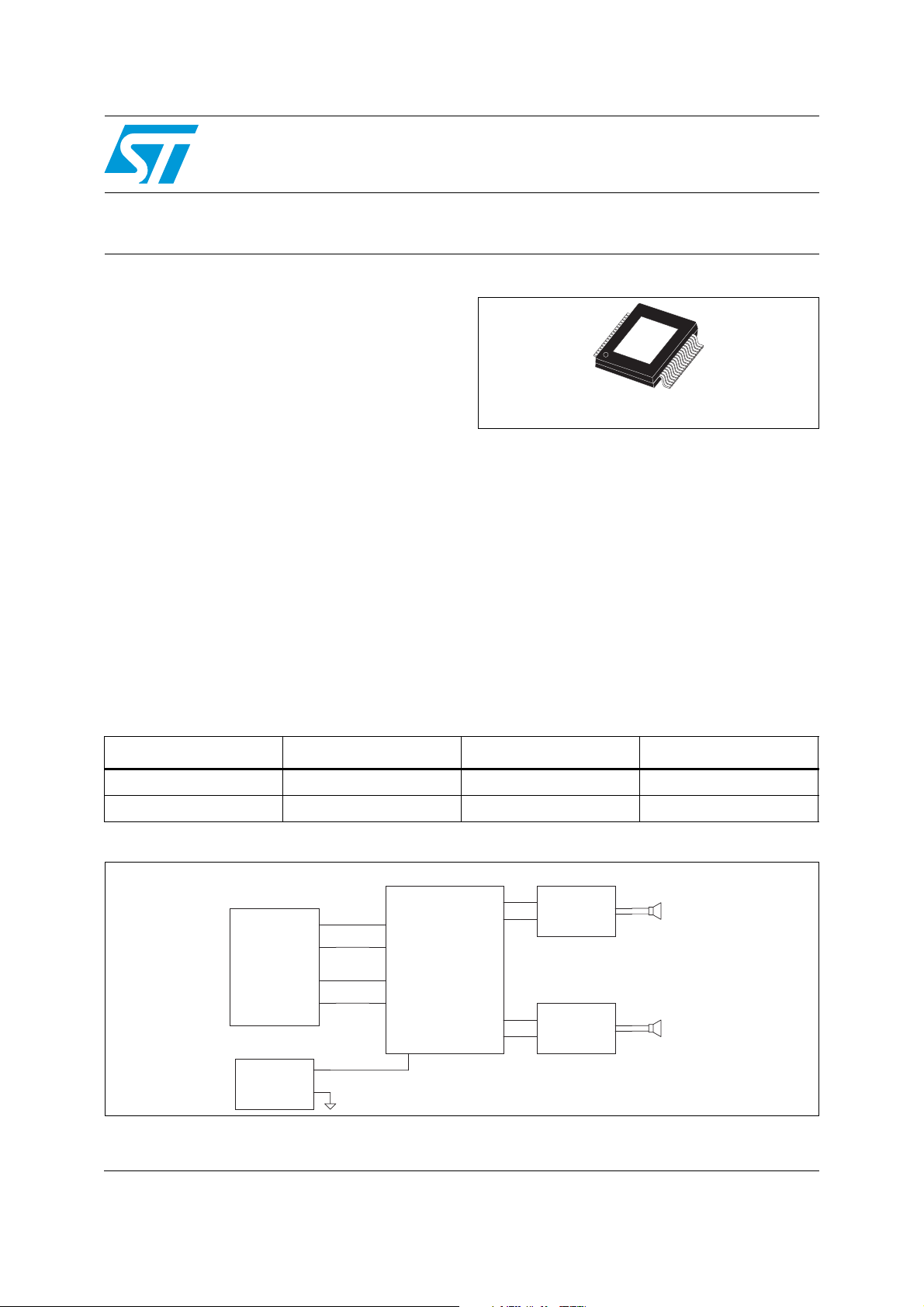
Table 1. Device summary
STA510F
44-V, 5.5-A, quad power half-bridge
PowerSSO36 with
exposed pad (or slug) up
The device is particularly designed to make the
output stage of a stereo all-digital high-efficiency
(FFX) amplifier capable of delivering 100 W +
100 W output power into 8-Ω loads with
THD = 10% and V
configuration the device can deliver 200 W into a
4-Ω load with THD = 10% and V
The device is fully compatible with the DDX
driver device.
The input pins have a threshold proportional to V
pin voltage.
= 39 V. In single BTL
cc
= 39 V.
cc
®
L
Order code Operating temp. range Package Packing
STA510F 0° to 70° C PowerSSO36 (slug up) Tube
STA510FTR 0° to 70° C PowerSSO36 (slug up) Tape & Reel
Figure 1. Typical application
Output Filter
OUT 1A
PWM Out1_A
PWM Out2_A
PWM Out1_B
PWM Out2_B
Vcc
PSU
GND
IN 1A
IN 2A
IN 1B
IN 2B
Vcc
OUT 1B
STA510FSTA309A
OUT 2A
OUT 2B
September 2011 Doc ID 14268 Rev 3 1/11
IN A
OUT A
OUT B
IN B
Output Filter
IN A
OUT A
OUT B
IN B
SPEAKERSPEAKER
SPEAKERSPEAKER
www.st.com
11
Page 2
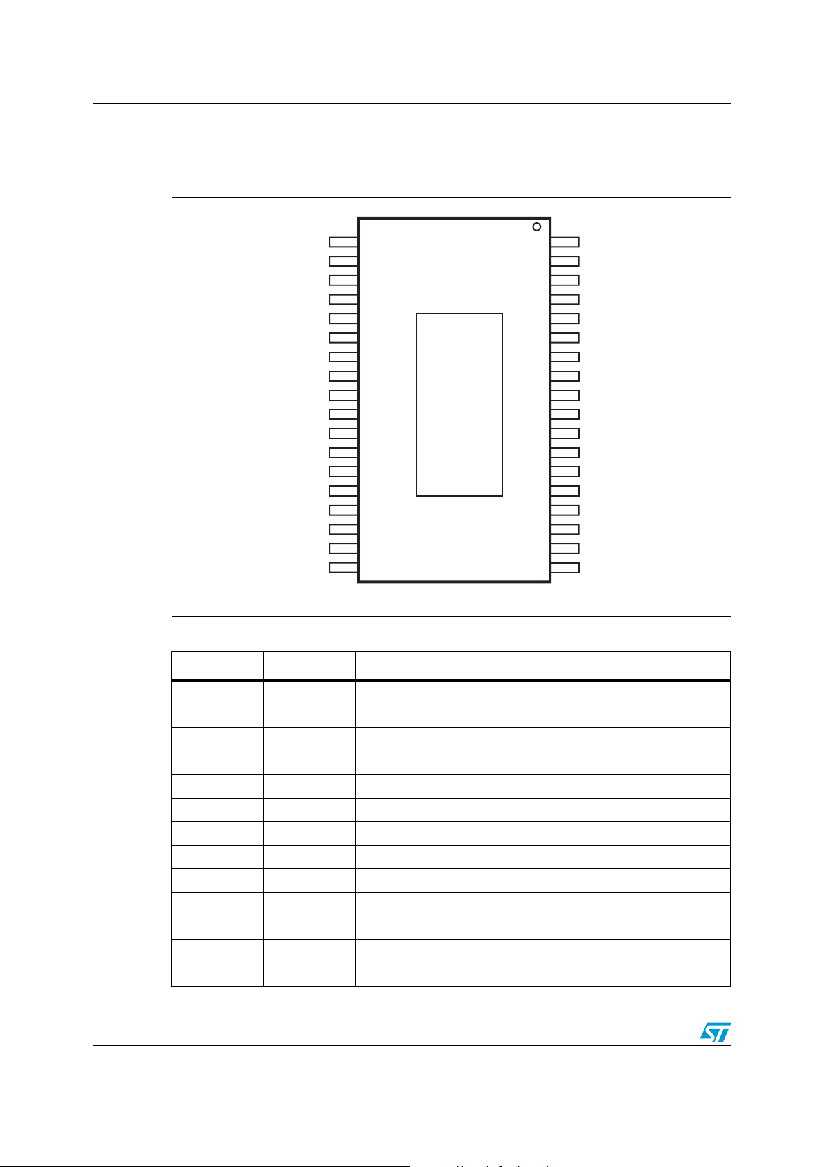
Pin description STA510F
1 Pin description
Figure 2. Pin connections (top view)
V
CC
VCCSign
FAULT
TRI-STATE
PWRDN
CONFIG
Table 2. Pin list
Sign
V
SS
V
SS
IN2B
IN1B
IN1A
V
V
DD
V
DD
1027
11
12
1324
14
15
16
17
18
1
2
3
4
5
6
7
8
9
GND-SUB
OUT2B
OUT2B
2B
V
CC
GND2B
GND2AIN2A
V
2A
CC
OUT2A
OUT2ATH_WAR
OUT1B
OUT1B
V
1B
CC
GND1B
GND1A
V
1A
CC
OUT1A
OUT1AGND-Reg
N.C.GND-Clean
36
35
34
33
32
31
30
29
28
26
25
L
23
22
21
20
19
Pin Name Description
1 GND-SUB Substrate ground
2, 3 OUT2B Output half-bridge 2B
4 Vcc2B Positive supply
5 GND2B Negative supply
6 GND2A Negative supply
7 Vcc2A Positive supply
8, 9 OUT2A Output half-bridge 2A
10, 11 OUT1B Output half-bridge 1B
12 Vcc1B Positive supply
13 GND1B Negative supply
14 GND1A Negative supply
15 Vcc1A Positive supply
16, 17 OUT1A Output half-bridge 1A
2/11 Doc ID 14268 Rev 3
Page 3
STA510F Pin description
Table 2. Pin list (continued)
Pin Name Description
18 NC Not connected
19 GND-clean Logical ground
20 GND-Reg Ground for regulator Vdd
21, 22 Vdd 5-V regulator referred to ground
23 V
L
High logical state setting voltage
24 CONFIG Configuration
25 PWRDN Standby
26 TRI-STATE Hi-Z
27 FAULT Fault pin advisor
28 TH-WAR Thermal warning advisor
29 IN1A Input of half-bridge 1A
30 IN1B Input of half-bridge 1B
31 IN2A Input of half-bridge 2A
32 IN2B Input of half-bridge 2B
33, 34 Vss 5-V regulator referred to +Vcc
35, 36 VCCSIGN Signal positive supply
Table 3. Pin values
Pin Logical value Device status
FAULT
(1)
0 Fault detected (short-circuit, or thermal)
1 Normal operation
0 All power stages in Hi-Z state
TRI-STATE
1 Normal operation
PWRDN
0 Low-power mode
1 Normal operation
THWAR
(1)
0 Temperature of the IC = 130° C
1 Normal operation
0 Normal operation
CONFIG
1. The pin is open collector. To have the high logic value, it needs a pull-up resistor.
2. CONFIG = 1 means connect pin 24 (CONFIG) to pins 21, 22 (Vdd).
(2)
1
OUT1A = OUT1B, OUT2A = OUT2B
(IF IN1A = IN1B and IN2A = IN2B)
Doc ID 14268 Rev 3 3/11
Page 4
Electrical specifications STA510F
2 Electrical specifications
2.1 Absolute maximum ratings
Table 4. Absolute maximum ratings
Symbol Parameter Value Unit
V
V
CC
max
DC supply voltage (pin 4, 7, 12, 15) 44 V
Maximum voltage on pins 23 to 32 5.5 V
ESD Max ESD on pins (HBM) ±1000 V
T
op
, T
T
stg
Operating temperature range 0 to 70 ° C
Storage and junction temperature -40 to 150 ° C
j
2.2 Thermal data
Table 5. Thermal data
Symbol Parameter Min Typ Max Unit
T
j-case
T
jSD
T
warn
t
hSD
Thermal resistance junction to case (thermal pad) 1 2.5 °C/W
Thermal shut-down junction temperature 150 ° C
Thermal warning temperature 130 ° C
Thermal shutdown hysteresis 25 ° C
2.3 Electrical specifications
The results in Ta bl e 6 below are given for the conditions: VL= 3.3 V, Vcc = 37 V and
T = 25° C unless otherwise specified.
Table 6. Electrical specifications
Symbol Parameter Condition Min Typ Max Unit
R
dsON
I
dss
g
N
g
P
Dt_s Low current deadtime (static) see test circuit Figure 3 10 20 ns
Dt_d High current deadtime (dynamic)
t
d ON
4/11 Doc ID 14268 Rev 3
Power Pchannel/Nchannel MOSFET
RdsON
Power Pchannel/Nchannel leakage
current
Id = 1 A 150 200 mΩ
100 μA
Power Pchannel RdsON matching Id = 1 A 95 %
Power Nchannel RdsON matching Id = 1 A 95 %
L = 22 μH, C = 470 nF,
RL = 8 Ω, Id = 4.5 A,
50 ns
see test circuit Figure 4
Turn-on delay time Resistive load 100 ns
Page 5

STA510F Electrical specifications
Table 6. Electrical specifications (continued)
Symbol Parameter Condition Min Typ Max Unit
t
d OFF
t
r
t
f
V
CC
V
IN-High
V
IN-Low
I
IN-H
I
IN-L
I
PWRDN-H
V
Low
V
High
I
VCC-
PWRDN
I
FAULT
I
VCC-hiz
I
VCC
Turn-off delay time Resistive load 100 ns
Rise time Resistive load, as Figure 4 25 ns
Fall time Resistive load, as Figure 4 25 ns
Supply voltage operating voltage 10 40 V
V
/2
+
High level input voltage
Low level input voltage
High level input current Pin voltage = V
L
L
300mV
V
/2 –
V
L
300mV
V
1 μA
Low level input current Pin voltage = 0.3 V 1 μA
High level PWRDN pin input current VL= 3.3 V 35 μA
Low logical state voltage (pins
PWRDN, TRISTATE) (see Tab l e 7 )
High logical state voltage (pins
PWRDN, TRISTATE) (see Tab l e 7 )
Supply current from Vcc in power
down
= 3.3 V 0.8 V
V
L
V
= 3.3 V 1.7 V
L
PWRDN = 0 3 mA
Output current pins
FAULT -TH-WARN when
FAULT CONDITIONS
Vpin = 3.3 V 1 mA
Supply current from Vcc in tri-state Pin TRI-STATE = 0 22 mA
Input pulse width duty
Supply current from Vcc in operation
both channel switching)
cycle = 50%,
switching frequency
= 384 kHz,
70 mA
no LC filters;
I
OUT-SH
V
UV
t
pw_min
Overcurrent protection threshold Isc
(short-circuit current limit)
5.5 7 9 A
Undervoltage protection threshold 7 V
Output minimum pulse width No load 25 40 ns
Doc ID 14268 Rev 3 5/11
Page 6

Electrical specifications STA510F
Table 7. V
V
, V
low
L
threshold variation with V
high
V
max V
Low
L
min Unit
High
2.7 0.7 1.5 V
3.3 0.8 1.7 V
5 0.85 1.85 V
Table 8. Logic truth table
TRI-STATE INxA INxB Q1 Q2 Q3 Q4 Output mode
0 xxOFFOFFOFFOFFHi-Z
1 00OFFOFFONONDUMP
1 0 1 OFF ON ON OFF NEGATIVE
1 1 0 ONOFFOFFONPOSITIVE
1 1 1 ON ON OFF OFF Not used
Figure 3. Test circuit for low current deadtime
OUTxY
Vcc
(3/4)Vcc
Low current dead time = MAX(DTr,DTf)
(1/2)Vcc
(1/4)Vcc
+Vcc
t
Duty cycle = 50%
INxY
M58
M57
gnd
OUTxY
R 8Ω
DTfDTr
+
V67 =
-
vdc = Vcc/2
D03AU1458
Figure 4. Test circuit for high current deadtime
High Current Dead time for Bridge application = ABS(DTout(A)-DTin(A))+ABS(DTOUT(B)-DTin(B))
+V
CC
Duty cycle=A Duty cycle=B
M58
DTin(A)
INxA
M57
Q1
OUTxA
Q3
DTout(A)
Iout=4.5A
C69
470nF
Rload=8Ω
C71 470nF
DTout(B) DTin(B)
L68 22μL67 22μ
Iout=4.5A
C70
470nF
Q2
OUTxB
Q4
M64
INxB
M63
Duty cycle A and B: Fixed to have DC output current of 4.5A in the direction shown in figure
6/11 Doc ID 14268 Rev 3
D00AU1162
Page 7

STA510F Electrical specifications
Figure 5. Typical quad half-bridge configuration giving 200 W per channel into 4 Ω speakers,
TH_W
EAPD
PWM
Input
IN 2B
IN 2A
IN 1B
IN 1A
3V3
10% THD, V
R2
R1
10KR210K
10kR110k
C11
C11
100n
100n
C8
100nC8100n
3V3
CC
=39V
C7
100nC7100n
C9
100nC9100n
C10
C10
100n
100n
36
35
34
33
32
31
30
29
28
27
26
25
24
23
22
21
20
19
STA510FSTA510F
VccSig
VccSig
Vss
Vss
IN2B
IN2A
IN1B
IN1A
TH_WARN
FAULT
TRISTATE
PWRDN
CONFIG
Ibias
Vdd
Vdd
GNDReg
GNDClean
GND Sub
OUT2B
OUT2B
Vcc2B
GND2B
GND2A
Vcc2A
OUT2A
OUT2A
OUT1B
OUT1B
Vcc1B
GND1B
GND1A
Vcc1A
OUT1A
OUT1A
L201
C201
C201
330p
330p
R20120R201
20
R20220R202
20
C202
C202
330p
330p
C101
C101
330p
330p
R10120R101
20
R10220R102
20
C102
C102
330p
330p
L201
15u
15u
L202
L202
15u
15u
L101
L101
L102
L102
C203
C203
C2051uC205
10n
10n
R20320R203
1u
20
R20420R204
20
C204
C204
10n
10n
C31uC3
1u
C51uC5
1u
15u
15u
C103
C103
10n
10n
R10320R103
20
R10420R104
20
C104
C104
10n
10n
15u
15u
C2061uC206
1u
C6
100nC6100n
C1051uC105
1u
C1061uC106
1u
C4
100nC4100n
C207
C207
330n
330n
C107
C107
330n
330n
C2
100nC2100n
4 ohm4 ohm
+
+
4 ohm4 ohm
C1
C1
1000u
1000u
Vcc
OUT2B
1
2
3
4
5
6
7
8
9
10
11
12
13
14
15
16
17
18
NC
OUT2A
OUT1B
OUT1A
Figure 6. Typical driving configuration with STA309A
Doc ID 14268 Rev 3 7/11
Page 8

Package information STA510F
3 Package information
In order to meet environmental requirements, ST offers these devices in different grades of
ECOPACK
specifications, grade definitions and product status are available at: www.st.com.
ECOPACK
®
packages, depending on their level of environmental compliance. ECOPACK®
®
is an ST trademark.
Figure 7. PowerSSO36 package dimensions
DIM.
A2.15 2.470.084 0.097
A2 2.15 2.40 0.084 0.094
a1 0 0.075 0 0.003
b 0.18 0.36 0.007 0.014
c0.23 0.32 0.009 0.012
(1)
D
(1)
E
e0.50 0.020
e38.50 0.035
F2.3 0.090
G 0.10 0.004
H 10.10 10.50 0.398 0.413
h 0.40 0.016
k
L0.55 0.85 0.022 0.033
M4.3 0.169
O 1.2 0.047
Q0.8 0.031
S 2.9 0.114
T 3 .65 0.144
U 1.0 0.039
X 4.10 4.70 0.161 0.185
Y 6.50 7.10 0.256 0.279
(1) “D and E” do not include mold flash or protusions.
Mold flash or protusions shall not exceed 0.15mm (0.006”) per side
(2) No intrusion allowed inwards the leads.
(3) Flash or bleeds on exposed die pad shall not exc eed 0.5 mm
per side
mm inch
MIN. TYP. MAX. MIN. TYP. MAX.
10.10 10.50 0.398 0.413
7.4 7.6 0.291 0.299
0° 8°0°
)xam( ˚01N
OUTLINE AND
MECHANICAL DATA
8°
PowerSSO-36
(slug-up)
8/11 Doc ID 14268 Rev 3
7618147_E
Page 9

STA510F Trademarks and other acknowledgements
4 Trademarks and other acknowledgements
FFX is a STMicroelectronics proprietary digital modulation technology.
DDX is a registered trademark of Apogee Technology, Inc.
ECOPACK is a registered trademark of STMicroelectronics.
Doc ID 14268 Rev 3 9/11
Page 10

Revision history STA510F
5 Revision history
Table 9. Document revision history
Date Revision Changes
13-Dec-2007 1 Initial release.
Added part number STA510FTR to Table 1: Device summary
28-Jun-2011 2
02-Sep-2011 3
Updated ECOPACK® text in Section 3: Package information
Minor textual updates
Updated package to PowerSSO36 throughout datasheet
Corrected typographical error in Features
Updated Figure 1: Typical application
Updated Figure 2: Pin connections (top view)
Updated Figure 6: Typical driving configuration with STA309A
Updated Figure 7: PowerSSO36 package dimensions
10/11 Doc ID 14268 Rev 3
Page 11

STA510F
Please Read Carefully:
Information in this document is provided solely in connection with ST products. STMicroelectronics NV and its subsidiaries (“ST”) reserve the
right to make changes, corrections, modifications or improvements, to this document, and the products and services described herein at any
time, without notice.
All ST products are sold pursuant to ST’s terms and conditions of sale.
Purchasers are solely responsible for the choice, selection and use of the ST products and services described herein, and ST assumes no
liability whatsoever relating to the choice, selection or use of the ST products and services described herein.
No license, express or implied, by estoppel or otherwise, to any intellectual property rights is granted under this document. If any part of this
document refers to any third party products or services it shall not be deemed a license grant by ST for the use of such third party products
or services, or any intellectual property contained therein or considered as a warranty covering the use in any manner whatsoever of such
third party products or services or any intellectual property contained therein.
UNLESS OTHERWISE SET FORTH IN ST’S TERMS AND CONDITIONS OF SALE ST DISCLAIMS ANY EXPRESS OR IMPLIED
WARRANTY WITH RESPECT TO THE USE AND/OR SALE OF ST PRODUCTS INCLUDING WITHOUT LIMITATION IMPLIED
WARRANTIES OF MERCHANTABILITY, FITNESS FOR A PARTICULAR PURPOSE (AND THEIR EQUIVALENTS UNDER THE LAWS
OF ANY JURISDICTION), OR INFRINGEMENT OF ANY PATENT, COPYRIGHT OR OTHER INTELLECTUAL PROPERTY RIGHT.
UNLESS EXPRESSLY APPROVED IN WRITING BY TWO AUTHORIZED ST REPRESENTATIVES, ST PRODUCTS ARE NOT
RECOMMENDED, AUTHORIZED OR WARRANTED FOR USE IN MILITARY, AIR CRAFT, SPACE, LIFE SAVING, OR LIFE SUSTAINING
APPLICATIONS, NOR IN PRODUCTS OR SYSTEMS WHERE FAILURE OR MALFUNCTION MAY RESULT IN PERSONAL INJURY,
DEATH, OR SEVERE PROPERTY OR ENVIRONMENTAL DAMAGE. ST PRODUCTS WHICH ARE NOT SPECIFIED AS "AUTOMOTIVE
GRADE" MAY ONLY BE USED IN AUTOMOTIVE APPLICATIONS AT USER’S OWN RISK.
Resale of ST products with provisions different from the statements and/or technical features set forth in this document shall immediately void
any warranty granted by ST for the ST product or service described herein and shall not create or extend in any manner whatsoever, any
liability of ST.
ST and the ST logo are trademarks or registered trademarks of ST in various countries.
Information in this document supersedes and replaces all information previously supplied.
The ST logo is a registered trademark of STMicroelectronics. All other names are the property of their respective owners.
© 2011 STMicroelectronics - All rights reserved
STMicroelectronics group of companies
Australia - Belgium - Brazil - Canada - China - Czech Republic - Finland - France - Germany - Hong Kong - India - Israel - Italy - Japan -
Malaysia - Malta - Morocco - Philippines - Singapore - Spain - Sweden - Switzerland - United Kingdom - United States of America
www.st.com
Doc ID 14268 Rev 3 11/11
 Loading...