

Page 1
Features
■ High output power capability
– 2x 38 W into 4 Ω at 18 V, 1 kHz, 10% THD
– 2x 34 W into 8 Ω at 22 V, 1 kHz, 10% THD
– 2x 24W into 4Ω at 14.4 V, 1 kHz, 10% THD
– 2x 15 W into 8 Ω at 16 V, 1 kHz, 10% THD
– 4x 13 W into 2 Ω at 15 V, 1 kHz, 10% THD
– 4x 11 W into 4 Ω at 18 V, 1 kHz, 10% THD
– 4x 7 W into 4 Ω at 14.4 V, 1 kHz, 10% THD
■ Minimum external components count:
– no bootstrap capacitors
– no Boucherot cells
– internally fixed gain 20 dB
■ Standby function (CMOS compatible)
■ No audible pop during standby operations
■ Diagnostic facilities:
– clip detector
– output to GND short-circuit detector
– output to VS short-circuit detector
– soft short-circuit check at turn-on
– thermal shutdown warning
STA540
4 x 13 W dual/quad power amplifier
Datasheet − production data
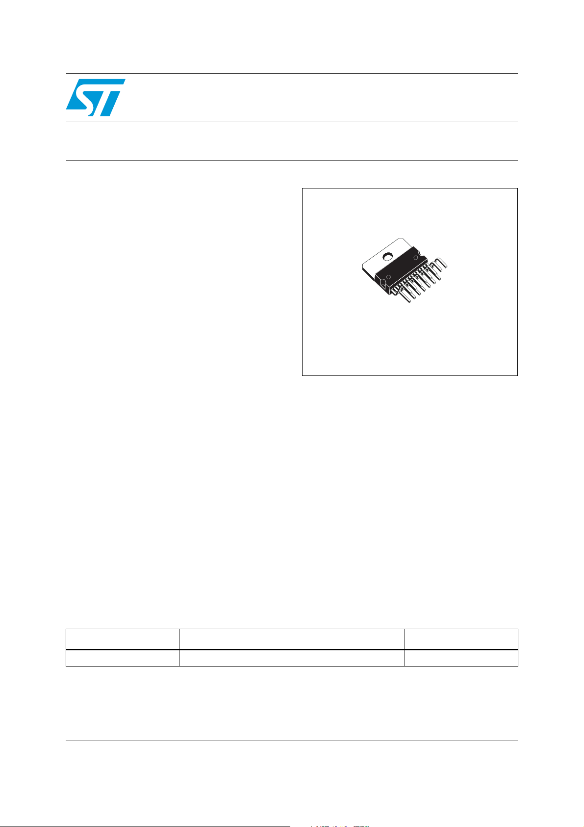
Multiwatt15
Description
The STA540 is a 4-channel, class-AB audio
amplifier designed for high quality sound
applications.
The amplifiers have single-ended outputs with
integrated short-circuit protection, thermal
protection and diagnostic functions.
Protection
■ Output AC/DC short circuit
■ Soft short-circuit check at turn-on
■ Thermal cutoff/limiter to prevent chip from
The chip is housed in the 15-pin Multiwatt
ECOPACK
®
Pb-free package which is RoHS
(2002/95/EC) compliant.
overheating
■ High inductive loads
■ ESD
Table 1. Device summary
Order code Temperature range Package Packing
STA540 -40 to 150° C Multiwatt15 Tube
April 2012 Doc ID 13907 Rev 6 1/25
This is information on a product in full production.
www.st.com
1
Page 2

Contents STA540
Contents
1 Block diagram and pin description . . . . . . . . . . . . . . . . . . . . . . . . . . . . . 6
1.1 Block diagram . . . . . . . . . . . . . . . . . . . . . . . . . . . . . . . . . . . . . . . . . . . . . . . 6
1.2 Pin description . . . . . . . . . . . . . . . . . . . . . . . . . . . . . . . . . . . . . . . . . . . . . . 7
2 Electrical specifications . . . . . . . . . . . . . . . . . . . . . . . . . . . . . . . . . . . . . . 8
2.1 Absolute maximum ratings . . . . . . . . . . . . . . . . . . . . . . . . . . . . . . . . . . . . . 8
2.2 Thermal data . . . . . . . . . . . . . . . . . . . . . . . . . . . . . . . . . . . . . . . . . . . . . . . 8
2.3 Electrical characteristics . . . . . . . . . . . . . . . . . . . . . . . . . . . . . . . . . . . . . . . 8
3 Standard application circuits . . . . . . . . . . . . . . . . . . . . . . . . . . . . . . . . . 10
4 Electrical characteristics curves . . . . . . . . . . . . . . . . . . . . . . . . . . . . . . 12
5 Thermal information . . . . . . . . . . . . . . . . . . . . . . . . . . . . . . . . . . . . . . . . 15
5.1 Heatsink specification examples . . . . . . . . . . . . . . . . . . . . . . . . . . . . . . . 15
5.1.1 R
5.1.2 R
5.1.3 Calculations using music power . . . . . . . . . . . . . . . . . . . . . . . . . . . . . . . 16
calculation for 4 single-ended channels . . . . . . . . . . . . . . . . . . . 15
th_HS
calculation for 2 single-ended channels plus 1 BTL channel . . . 15
th_HS
6 Practical information . . . . . . . . . . . . . . . . . . . . . . . . . . . . . . . . . . . . . . . . 17
6.1 Highly flexible amplifier configuration . . . . . . . . . . . . . . . . . . . . . . . . . . . . 17
6.2 Easy single-ended to bridge transition . . . . . . . . . . . . . . . . . . . . . . . . . . . 17
6.3 Internally fixed gain . . . . . . . . . . . . . . . . . . . . . . . . . . . . . . . . . . . . . . . . . 17
6.4 Silent turn on/off and muting/standby function . . . . . . . . . . . . . . . . . . . . . 17
6.5 Driving circuit for standby mode . . . . . . . . . . . . . . . . . . . . . . . . . . . . . . . . 17
6.6 Output stage . . . . . . . . . . . . . . . . . . . . . . . . . . . . . . . . . . . . . . . . . . . . . . . 18
6.6.1 Rail-to-rail output voltage swing without bootstrap capacitors . . . . . . . . 18
6.6.2 Absolute stability without external compensation . . . . . . . . . . . . . . . . . 18
6.7 Built–in protection . . . . . . . . . . . . . . . . . . . . . . . . . . . . . . . . . . . . . . . . . . . 19
6.7.1 Diagnostic facilities (pin 10) . . . . . . . . . . . . . . . . . . . . . . . . . . . . . . . . . . 19
6.7.2 Short-circuit protection . . . . . . . . . . . . . . . . . . . . . . . . . . . . . . . . . . . . . . 19
6.7.3 Clipping detection . . . . . . . . . . . . . . . . . . . . . . . . . . . . . . . . . . . . . . . . . 20
6.7.4 Thermal shutdown . . . . . . . . . . . . . . . . . . . . . . . . . . . . . . . . . . . . . . . . . 20
2/25 Doc ID 13907 Rev 6
Page 3

STA540 Contents
6.8 Handling the diagnostic information . . . . . . . . . . . . . . . . . . . . . . . . . . . . . 21
6.9 PCB ground layout . . . . . . . . . . . . . . . . . . . . . . . . . . . . . . . . . . . . . . . . . . 22
6.10 Mute function . . . . . . . . . . . . . . . . . . . . . . . . . . . . . . . . . . . . . . . . . . . . . . 22
7 Package information . . . . . . . . . . . . . . . . . . . . . . . . . . . . . . . . . . . . . . . . 23
8 Revision history . . . . . . . . . . . . . . . . . . . . . . . . . . . . . . . . . . . . . . . . . . . 24
Doc ID 13907 Rev 6 3/25
Page 4

List of tables STA540
List of tables
Table 1. Device summary . . . . . . . . . . . . . . . . . . . . . . . . . . . . . . . . . . . . . . . . . . . . . . . . . . . . . . . . . . 1
Table 2. Pin description . . . . . . . . . . . . . . . . . . . . . . . . . . . . . . . . . . . . . . . . . . . . . . . . . . . . . . . . . . . 7
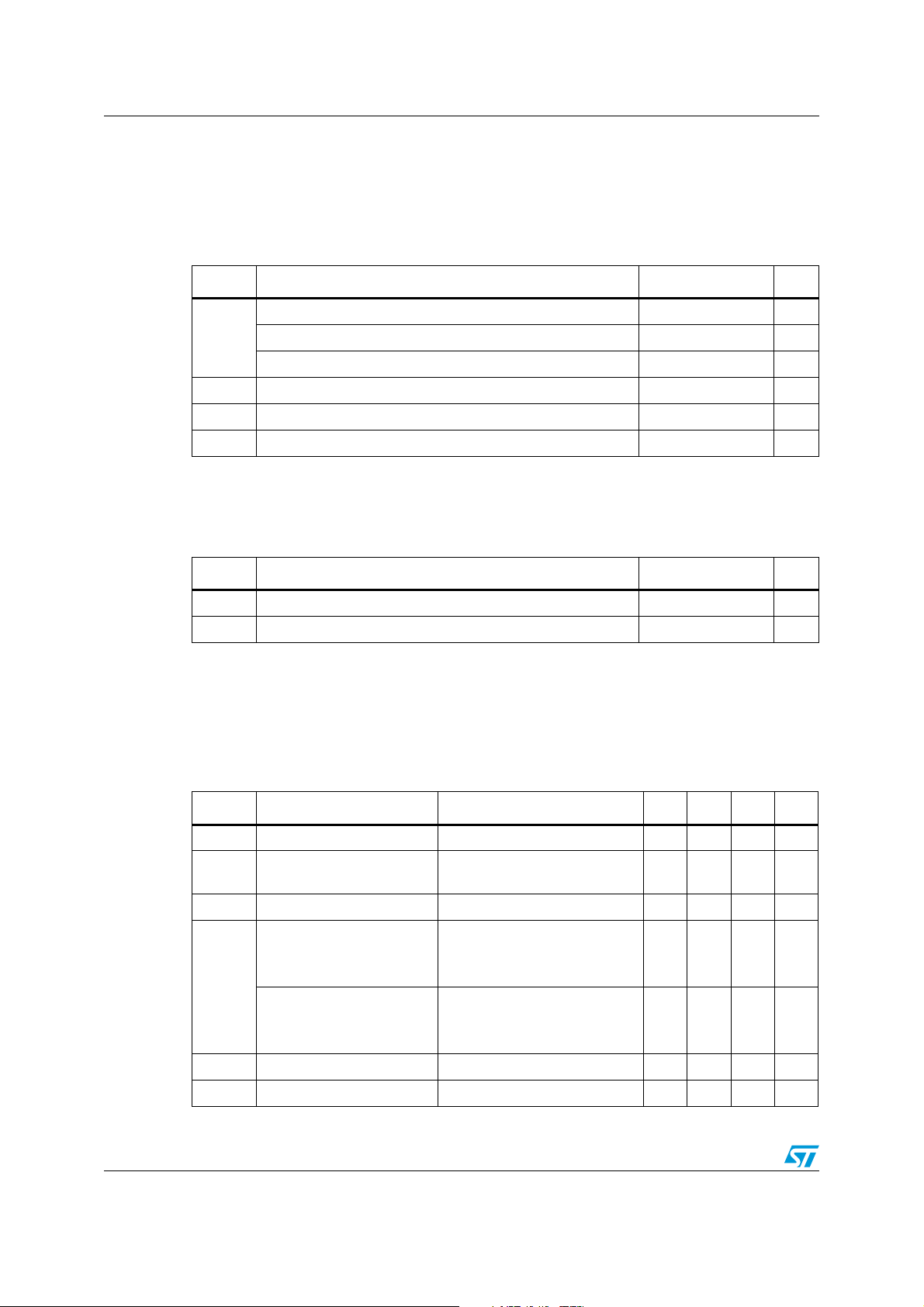
Table 3. Absolute maximum ratings . . . . . . . . . . . . . . . . . . . . . . . . . . . . . . . . . . . . . . . . . . . . . . . . . . 8
Table 4. Thermal data. . . . . . . . . . . . . . . . . . . . . . . . . . . . . . . . . . . . . . . . . . . . . . . . . . . . . . . . . . . . . 8
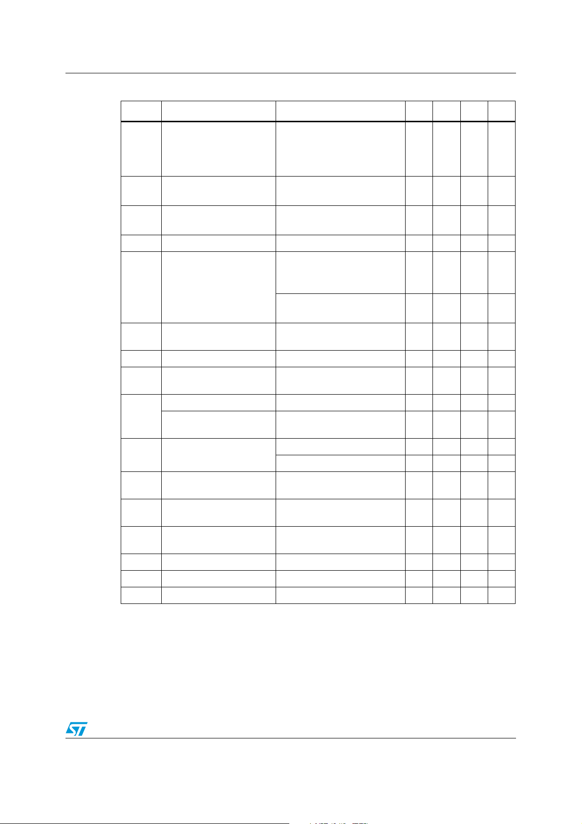
Table 5. Electrical characteristics . . . . . . . . . . . . . . . . . . . . . . . . . . . . . . . . . . . . . . . . . . . . . . . . . . . . 8
Table 6. Document revision history . . . . . . . . . . . . . . . . . . . . . . . . . . . . . . . . . . . . . . . . . . . . . . . . . 24
4/25 Doc ID 13907 Rev 6
Page 5

STA540 List of figures
List of figures
Figure 1. Block diagram . . . . . . . . . . . . . . . . . . . . . . . . . . . . . . . . . . . . . . . . . . . . . . . . . . . . . . . . . . . . 6
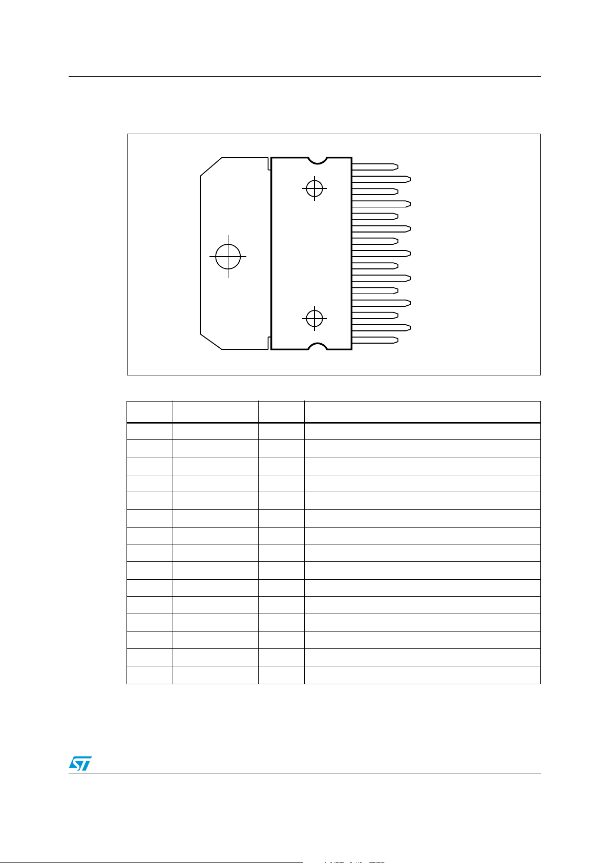
Figure 2. Pin connection (top view) . . . . . . . . . . . . . . . . . . . . . . . . . . . . . . . . . . . . . . . . . . . . . . . . . . . 7
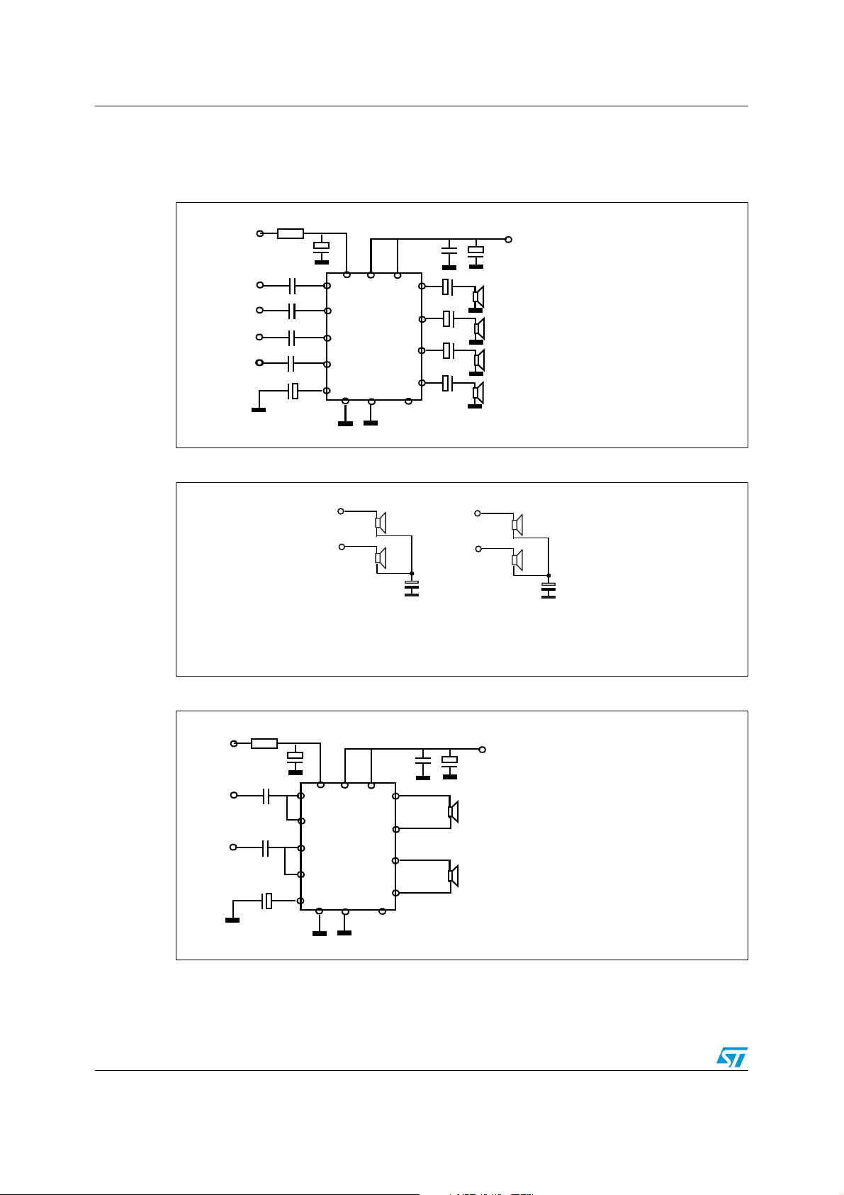
Figure 3. Quadraphonic . . . . . . . . . . . . . . . . . . . . . . . . . . . . . . . . . . . . . . . . . . . . . . . . . . . . . . . . . . 10
Figure 4. Alternative single-ended speaker connection . . . . . . . . . . . . . . . . . . . . . . . . . . . . . . . . . . 10
Figure 5. Dual bridge . . . . . . . . . . . . . . . . . . . . . . . . . . . . . . . . . . . . . . . . . . . . . . . . . . . . . . . . . . . . 10
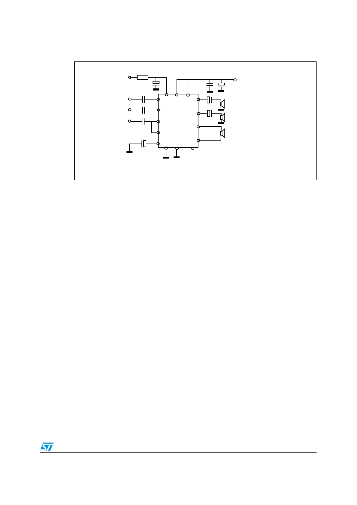
Figure 6. Stereo plus bridge drive . . . . . . . . . . . . . . . . . . . . . . . . . . . . . . . . . . . . . . . . . . . . . . . . . . . 11
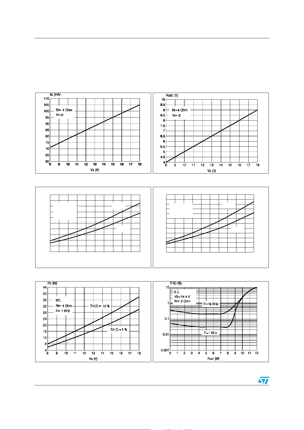
Figure 7. Quiescent drain current versus supply voltage (single-ended and bridge). . . . . . . . . . . . . 12
Figure 8. Quiescent output voltage versus supply voltage (single-ended and bridge). . . . . . . . . . . . 12
Figure 9. Output power versus supply voltage. . . . . . . . . . . . . . . . . . . . . . . . . . . . . . . . . . . . . . . . . . 12
Figure 10. Output power versus supply voltage. . . . . . . . . . . . . . . . . . . . . . . . . . . . . . . . . . . . . . . . . . 12
Figure 11. Output power versus supply voltage. . . . . . . . . . . . . . . . . . . . . . . . . . . . . . . . . . . . . . . . . . 12
Figure 12. Distortion versus output power . . . . . . . . . . . . . . . . . . . . . . . . . . . . . . . . . . . . . . . . . . . . . . 12
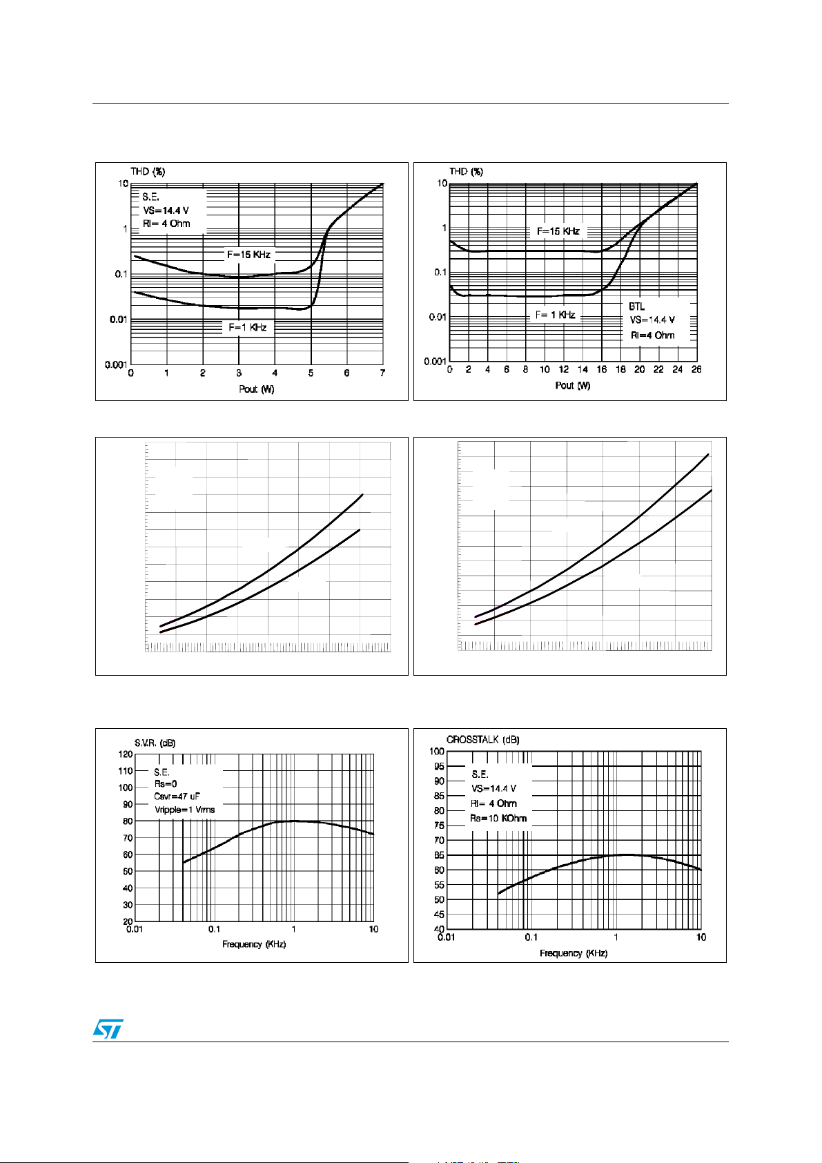
Figure 13. Distortion versus output power . . . . . . . . . . . . . . . . . . . . . . . . . . . . . . . . . . . . . . . . . . . . . . 13
Figure 14. Distortion versus output power . . . . . . . . . . . . . . . . . . . . . . . . . . . . . . . . . . . . . . . . . . . . . . 13
Figure 15. Output power versus supply voltage. . . . . . . . . . . . . . . . . . . . . . . . . . . . . . . . . . . . . . . . . . 13
Figure 16. Output power versus supply voltage. . . . . . . . . . . . . . . . . . . . . . . . . . . . . . . . . . . . . . . . . . 13
Figure 17. Supply voltage rejection versus frequency . . . . . . . . . . . . . . . . . . . . . . . . . . . . . . . . . . . . . 13
Figure 18. Crosstalk versus frequency . . . . . . . . . . . . . . . . . . . . . . . . . . . . . . . . . . . . . . . . . . . . . . . . 13
Figure 19. Standby attenuation versus threshold voltage . . . . . . . . . . . . . . . . . . . . . . . . . . . . . . . . . . 14
Figure 20. Total power dissipation and efficiency versus output power . . . . . . . . . . . . . . . . . . . . . . . . 14
Figure 21. Total power dissipation and efficiency versus output power . . . . . . . . . . . . . . . . . . . . . . . . 14
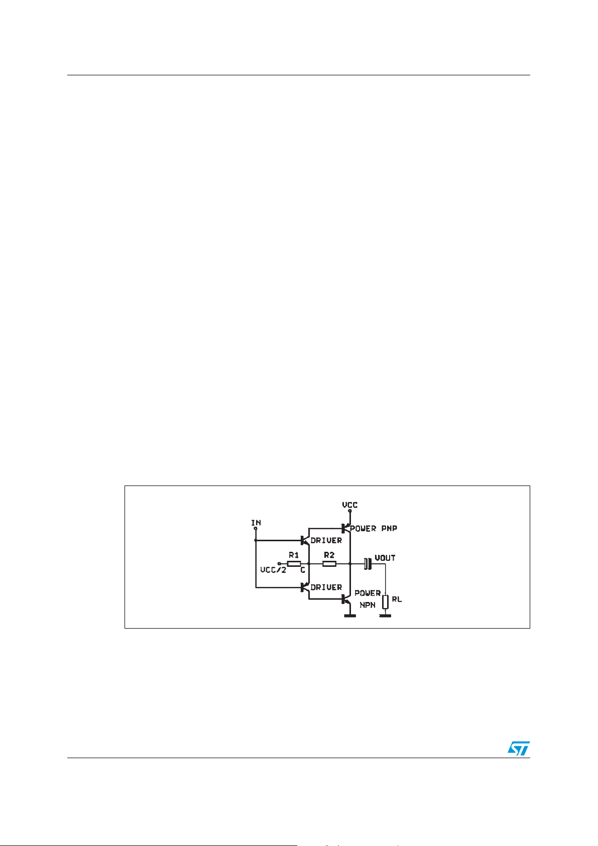
Figure 22. The new output stage . . . . . . . . . . . . . . . . . . . . . . . . . . . . . . . . . . . . . . . . . . . . . . . . . . . . 18
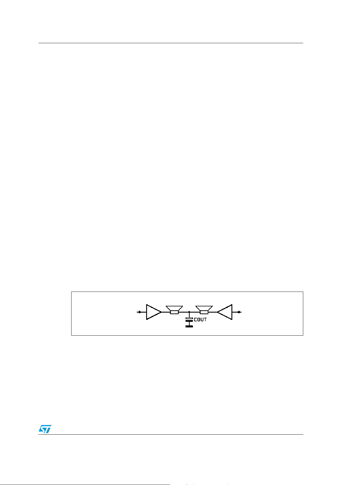
Figure 23. Shared capacitor in single-ended configuration . . . . . . . . . . . . . . . . . . . . . . . . . . . . . . . . . 19
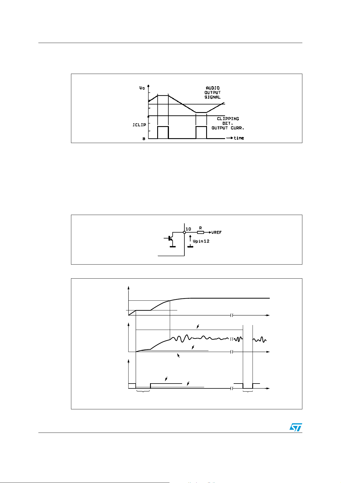
Figure 24. Clipping detection waveforms . . . . . . . . . . . . . . . . . . . . . . . . . . . . . . . . . . . . . . . . . . . . . . 20
Figure 25. Output fault waveforms (see Figure 26) . . . . . . . . . . . . . . . . . . . . . . . . . . . . . . . . . . . . . . . 20
Figure 26. Fault waveforms . . . . . . . . . . . . . . . . . . . . . . . . . . . . . . . . . . . . . . . . . . . . . . . . . . . . . . . . 20
Figure 27. Waveforms . . . . . . . . . . . . . . . . . . . . . . . . . . . . . . . . . . . . . . . . . . . . . . . . . . . . . . . . . . . . . 21
Figure 28. Interface circuit diagram . . . . . . . . . . . . . . . . . . . . . . . . . . . . . . . . . . . . . . . . . . . . . . . . . . . 21
Figure 29. Optional mute function circuit . . . . . . . . . . . . . . . . . . . . . . . . . . . . . . . . . . . . . . . . . . . . . . 22
Figure 30. Mechanical data and package dimensions (Multiwatt15) . . . . . . . . . . . . . . . . . . . . . . . . . 23
Doc ID 13907 Rev 6 5/25
Page 6

Block diagram and pin description STA540
1 Block diagram and pin description
1.1 Block diagram
Figure 1. Block diagram
VCC1VCC2
V
CC2VCC1
IN1
ST-BY
ST-BY
IN2
IN3
IN4
13
4
7
5
12
11
3
689
SVR P-GND S-GND
A1
+
-
A2 INV
+
-
A3
+
-
A4 INV
+
-
1
2
15
14
10
OUT1
OUT2
OUT3
OUT4
DIAGNOSTIC
DIAGNOSTICD
OUTPUT
D06AU1630
6/25 Doc ID 13907 Rev 6
Page 7
STA540 Block diagram and pin description
1.2 Pin description
Figure 2. Pin connection (top view)
OUT3
15
14
13
12
11
10
9
8
7
6
5
4
3
2
1
OUT3
OUT4
OUT4
VCC2
VCC
IN3
IN3
IN4
IN4
DIAGNOSTICD
DIAGNOSTICD
S-GND
S-GND
P-GND
PW-GND
ST-BY
STAND-BY
SVR
SVR
IN2
IN2
IN1
IN1
VCC1
VCC
OUT2
OUT2
OUT1
OUT1
D06au1631
Table 2. Pin description
N° Name Type Function
1 OUT1 OUT Channel 1 output
2 OUT2 OUT Channel 2 output
3 VCC1 PWR Power supply
4 IN1 IN Channel 1 input
5 IN2 IN Channel 2 input
6 SVR IN Supply voltage rejection
7 ST-BY IN Standby control pin
8 P-GND PWR Power ground
9 S-GND PWR Signal ground
10 DIAGNOSTICD OUT Diagnostics output
11 IN4 IN Channel 4 input
12 IN3 IN Channel 3 input
13 VCC2 PWR Power supply
14 OUT4 OUT Channel 4 output
15 OUT3 OUT Channel 3 output
Doc ID 13907 Rev 6 7/25
Page 8
Electrical specifications STA540
2 Electrical specifications
2.1 Absolute maximum ratings
Table 3. Absolute maximum ratings
Symbol Parameter Value Unit
Supply voltage idle mode (no signal) 24 V
V
Supply voltage operating 22 V
s
Supply voltage AC-DC short safe 20 V
P
T
stg
Total power dissipation (T
tot
case
, TjStorage and junction temperature -40 to150 °C
Operating temperature 0 to 70 °C
T
op
2.2 Thermal data
Table 4. Thermal data
Symbol Parameter Value Unit
R
th j-case
R
th j-amb
Thermal resistance junction to case (max) 1.8 °C/W
Thermal resistance junction to ambient (max) 35 °C/W
2.3 Electrical characteristics
The test conditions are VS = 14.4 V, RL = 4 Ω, f = 1 kHz, T
specified.
Table 5. Electrical characteristics
Symbol Parameter Test condition Min Typ Max Unit
V
Supply voltage range 8 22 V
S
Total quiescent drain
I
d
current
V
Output offset voltage -150 150 mV
os
Output power, SE
P
o
Output power, BTL
= 85 °C) 36 W
= 25° C unless otherwise
amb
80 150 mA
THD=10%, R
THD=10%, R
THD=10%, R
THD=10%, R
THD=10%, R
=4 Ω
L
=2 Ω
L
=4 Ω, VS=22 V
L
=4 Ω
L
=8 Ω, VS=17 V
L
THD=10%, RL=8 Ω, VS=22 V
6.5
21
7
11.5
16
24
20
34
W
W
THD Total harmonic distortion R
Short-circuit output current 4.0 A
I
SC
= 4 Ω, Po = 0.1 to 4 W 0.02 %
L
8/25 Doc ID 13907 Rev 6
Page 9
STA540 Electrical specifications
Table 5. Electrical characteristics (continued)
Symbol Parameter Test condition Min Typ Max Unit
Crosstalk
C
T
Input impedance Single-ended BTL
R
in
G
Voltage gain Single-ended BTL
v
G
Voltage gain match 0.5 dB
v
E
Input noise voltage
N
SVR Supply voltage rejection
A
Standby attenuation Po = 1 W 80 90 dB
SB
Current consumption in
I
SB
standby
ST-BY IN threshold voltage 1.5 V
V
SB
ST-BY OUT threshold
voltage
f = 1 kHz single-ended
f = 10 kHz single-ended
f = 1 kHz BTL
f = 10 kHz BTL
= 0, "A" weighted, S.E.:
R
gen
Non-inverting channels
Inverting channels
BTL
= 0, f = 22 Hz to 22 kHz
R
gen
= 0, f = 300 Hz,
R
gen
C
= 470 μF
SVR
V
= 0 to 1.5 V 100 μA
ST_BY
70
60
55
dB
60
201030
15
1925202621
2
5
27
kΩ
dB
μV
μV
3.5 μV
50 dB
3.5 V
I
ST-BY
I
cd_off
I
cd_on
V
DIAGNO
STICD
T
T
T
Pin ST-BY current
Play mode, V
= 5 V 50 μA
ST-BY
Max driving current under fault 5 mA
Clipping detector output
average current
Clipping detector output
average current
Saturation voltage on pin
DIAGNOSTICD
Thermal warning 140 °C
W
Thermal muting 150 °C
M
Thermal shutdown 160 °C
S
d = 1% (*) 90 μA
d = 5% (*) 160 μA
I
DIAGNOSTICD
= 1 mA sinking 0.7 V
Doc ID 13907 Rev 6 9/25
Page 10
Standard application circuits STA540
3 Standard application circuits
Figure 3. Quadraphonic
ST_BY
IN_1
IN_2
IN_3
IN_4
10 kΩ
10 µF
220 nF
220 nF
220 nF
220 nF
47 µF
13
STA540
3
7
4
5
12
11
6
89 10
100 nF
1
2
15
14
2200 µF
2200 µF
2200 µF
2200 µF
1000 µF
OUT_1
OUT_2
OUT_3
OUT_4
V
S
Figure 4. Alternative single-ended speaker connection
1
*
1
2
2
The best audio performance is obtained with the configuration where each speaker
has its own DC blocking capacitor. However, if the application allows a little
degradation of the spatial image it is possible to connect a couple of speakers with
only one low-value DC blocking capacitor.
470μF
18
15
19
14
Suggested applications:
4x 13 W into 2 Ω, at 15 V
4x 11 W into 4 Ω, at 18 V
4x 9 W into 2 Ω, at 12 V
4x 8 W into 4 Ω, at 16 V
4x 5 W into 4 Ω, at 12 V
470μF
Figure 5. Dual bridge
ST_BY
IN_L
IN_R
10/25 Doc ID 13907 Rev 6
10 kΩ
10 µF
470 nF
470 nF
47 µF
13
STA540
3
7
4
5
12
11
6
89 10
100 nF
1
2
15
14
1000 µF
OUT_R
OUT_L
Suggested applications:
V
S
2x 38 W into 4 Ω, at 18 V, 1 kHz, 10% THD
2x 34 W into 8 Ω, at 22 V, 1 kHz, 10% THD
2x 24 W into 4 Ω, at 14.4 V, 1 kHz, 10% THD
2x 15 W into 8 Ω, at 16 V, 1 kHz, 10% THD
Page 11
STA540 Standard application circuits
Figure 6. Stereo plus bridge drive
ST_BY
IN_L
IN_R
IN_Bridge
10 kΩ
10 µF
220 nF
220 nF
470 nF
47 µF
7
4
5
3
13
STA540
12
11
6
89 10
V
100 nF
1
2200 µF
2
2200 µF
15
S
1000 µF
OUT_L
OUT_R
OUT_Bridge
14
Suggested applications:
2x 9 W into 2 Ω, +1x 18 W into 4 Ω, at 12 V
2x 12 W into 2 Ω, +1x 26 W into 4 Ω, at 14.4 V
2x 8 W into 4 Ω, +1x 16 W into 8 Ω, at 16 V
Doc ID 13907 Rev 6 11/25
Page 12
Electrical characteristics curves STA540
4 Electrical characteristics curves
Figure 7. Quiescent drain current versus
supply voltage (single-ended and
bridge)
Figure 8. Quiescent output voltage versus
supply voltage (single-ended and
bridge)
Figure 9. Output power versus supply voltage Figure 10. Output power versus supply voltage
Po ( W)
20
18
16
14
12
SINGLE ENDED
Ω
RL= 2
f= 1 KHz
THD= 10 %
10
8
THD= 1 %
6
4
2
0
8 9 10 11 12 13 14 15 16 17 18
Vs (V)
Po (W)
12
11
10
9
8
7
SINGLE ENDED
RL= 4
Ω
f= 1 KHz
THD= 10 %
6
5
THD= 1 %
4
3
2
1
0
8 9 10 11 12 13 14 15 16 17 18
Vs (V)
Figure 11. Output power versus supply voltage Figure 12. Distortion versus output power
12/25 Doc ID 13907 Rev 6
Page 13
STA540 Electrical characteristics curves
4
4
Figure 13. Distortion versus output power Figure 14. Distortion versus output power
Figure 15. Output power versus supply voltage Figure 16. Output power versus supply voltage
12
12
Po(W)
Po(W)
11
11
S.E.
S.E.
10
10
Rl=8ohm
Rl=8ohm
9
9
f=1KHz
f=1KHz
8
8
7
7
T.H. D=1 0%
6
6
5
5
4
4
3
3
2
2
1
1
0
0
+8 +2
+8 +2
+10 + 12 +14 +16 +18 +20 +22
+10 + 12 +14 +16 +18 +20 +22
T.H. D=1 0%
Vs(V)
Vs(V)
T.H. D=1 %
T.H. D=1 %
Figure 17. Supply voltage rejection versus
35
35
Po(W)
Po(W)
32.5
32.5
30
30
BTL
BTL
27.5
27.5
Rl=8ohm
Rl=8ohm
25
25
f=1KHz
f=1KHz
22.5
22.5
20
20
17.5
17.5
15
15
12.5
12.5
10
10
7.5
7.5
5
5
2.5
2.5
0
0
+8 +22+10 +12 +14 +16 +18 +20
+8 +22+10 +12 +14 +16 +18 +20
T.H.D=10 %
T.H.D=10 %
Vs(V)
Vs(V)
T.H.D=1%
T.H.D=1%
Figure 18. Crosstalk versus frequency
frequency
Doc ID 13907 Rev 6 13/25
Page 14
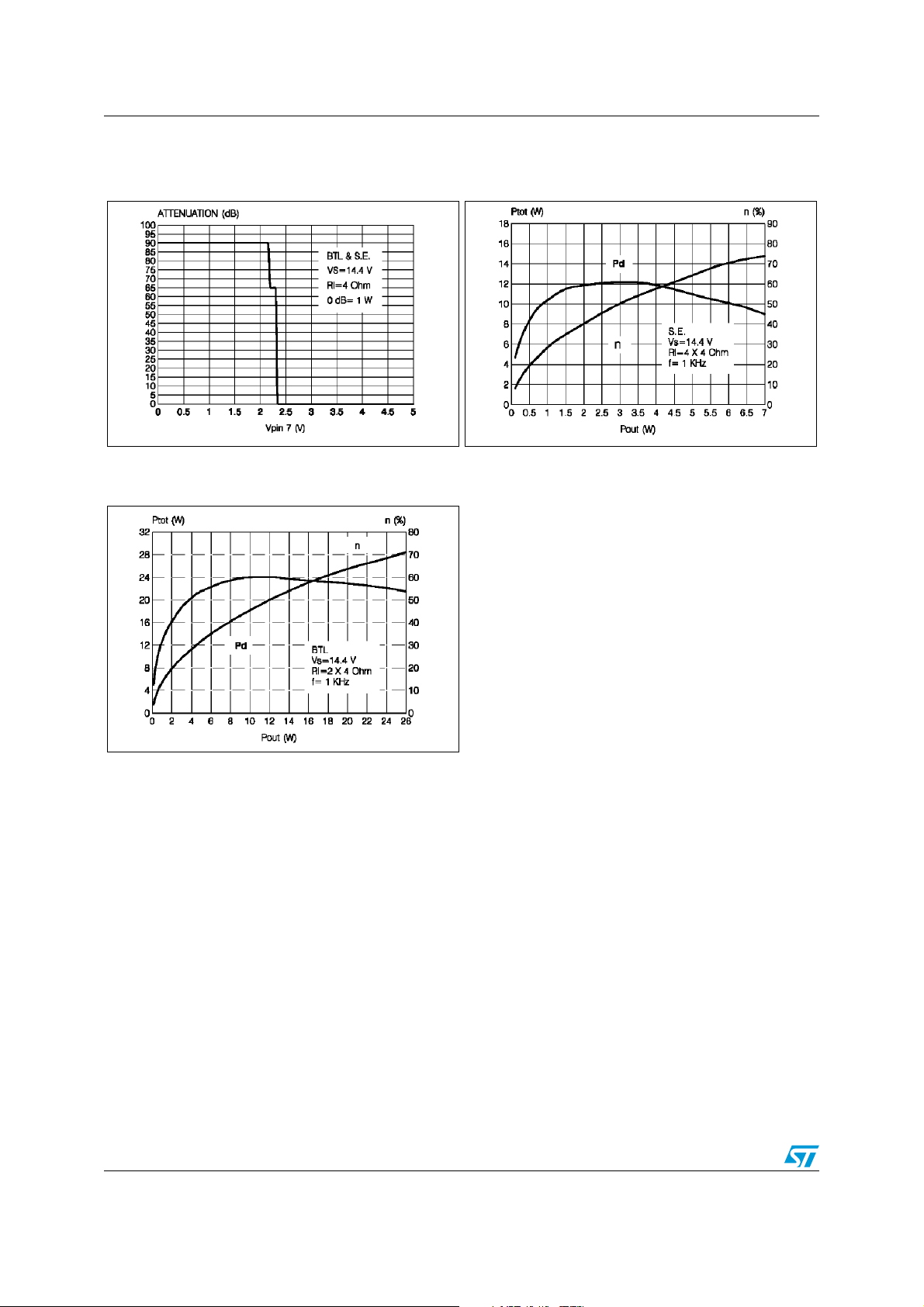
Electrical characteristics curves STA540
Figure 19. Standby attenuation versus
threshold voltage
Figure 21. Total power dissipation and
efficiency versus output power
Figure 20. Total power dissipation and
efficiency versus output power
14/25 Doc ID 13907 Rev 6
Page 15

STA540 Thermal information
5 Thermal information
In order to avoid the intervention of the thermal protection, placed at Tj =150° C for thermal
muting and T
resistance, R
The parameters that influence the calculation are:
● maximum dissipated power for the device (P
● maximum thermal resistance junction to case (R
● maximum ambient temperature T
There is also an additional term that depends on the Iq (quiescent current).
5.1 Heatsink specification examples
=160° C for thermal shutdown, it is important to calculate the heatsink thermal
j
, correctly.
th_HS
)
d
max
th_j-case
amb_max
)
5.1.1 R
Given VS = 14.4 V, RL = 4 Ω x 4 channels, R
P
the maximum power dissipated in the device is:
and the required thermal resistance of the heatsink is:
5.1.2 R
Given VS = 14.4 V, RL = 2x 2 Ω (SE) + 1x 4 Ω (BTL), P
the maximum power dissipated in the device is:
calculation for 4 single-ended channels
th_HS
= 4 x 7 W then
out
calculation for 2 single-ended channels plus 1 BTL channel
th_HS
R
th_HS
P
dmax
P
dmax
NChannel
150 T
–
--------------------------------------------- - R
amb_max
P
dmax
2
2
V
CC
------------------- -
2Π2R
V
------------------- - 4 2.62 10.5W=⋅=⋅=
2Π2R
L
th_j-case
2
CC
L
th_j-case
2
2V
CC
-------------------- 25.25 10.5 21W=+⋅=+⋅=
Π2R
L
= 1.8° C/W, T
150 50–
---------------------- 1.8 7.7° C/W=–=–=
10.5
= 2 x 12 W + 1 x 26 W then
out
amb_max
= 50° C and
and the required thermal resistance of the heatsink is:
150 T
–
R
th_HS
--------------------------------------------- - R
amb_max
P
dmax
Doc ID 13907 Rev 6 15/25
th_j-case
150 50–
---------------------- 1.8 3°C/W=–=–=
21
Page 16

Thermal information STA540
5.1.3 Calculations using music power
The thermal resistance value calculated in each of the two above examples specifies a
heatsink capable of sustaining the maximum dissipated power. Realistically, however, and
as explained in the Application Note (AN1965), the heatsink can be smaller when the
application is musical content.
When music power is considered the resulting dissipation is about 40% less than the
calculated maximum. Thus, smaller or cheaper heatsinks can be employed. The heatsink
thermal resistance values are modified as follows:
for example 5.1.1: 10.5 W - 40% = 6.3 W, thus giving R
for example 5.1.2: 21 W - 40% = 12.6 W, thus giving R
th_c-amb
th_c-amb
= 14° C/W,
= 6° C/W.
16/25 Doc ID 13907 Rev 6
Page 17

STA540 Practical information
6 Practical information
6.1 Highly flexible amplifier configuration
The availability of four independent channels makes it possible to accomplish several kinds
of applications ranging from four speakers stereo (F/R) to two-speaker bridge solutions.
When working with single-ended configurations, the polarity of the speakers driven by the
inverting amplifier must be reversed with respect to those driven by non-inverting channels.
This is to avoid phase irregularities causing sound alterations especially during the
reproduction of low frequencies.
6.2 Easy single-ended to bridge transition
The change from single-ended to bridge configuration is made simple by connecting the two
inputs together and also the speaker directly between the two outputs (no need for
additional external components, in fact the output DC blocking capacitors are eliminated).
However, take care to use an inverting/non-inverting amplifier pair.
6.3 Internally fixed gain
The advantages in internally fixing the gain (to 20 dB in single-ended configuration and to
26 dB in bridge configuration) are:
● components and space saving,
● output noise, supply voltage rejection and distortion optimization.
6.4 Silent turn on/off and muting/standby function
The standby mode can be easily activated by means of a CMOS logic level applied to
pin ST-BY through a RC filter.
Under standby conditions, the device is turned off completely (supply current = 1 mA typical,
output attenuation = 80 dB minimum).
All on/off operations are virtually pop-free. Furthermore, at turn-on the device stays in mute
condition for a time determined by the value of the SVR capacitor. This prevents transients,
coming from previous stages, from producing unpleasant acoustic effects at the speakers.
6.5 Driving circuit for standby mode
Some precautions need to be taken when designing the driving circuit for pin 7, ST-BY. For
instance, the pin cannot be directly driven by a voltage source having a current capability
higher than 5 mA. In practical cases a series resistance must be inserted, giving it the
double purpose of limiting the current at pin 7 and to smooth down the standby on/off
transitions. And, when done in combination with a capacitor, prevents output pop.
A capacitor of at least 100 nF from pin 7 to S-GND, with no resistance in between, is
necessary to ensure correct turn-on.
Doc ID 13907 Rev 6 17/25
Page 18
Practical information STA540
6.6 Output stage
The fully complementary output stage is possible with the power ICV PNP component.
This novel design is based on the connection shown in Figure 22 and allows the full
exploitation of its capabilities. The clear advantages this new approach has over classical
output stages are described in the following sections.
6.6.1 Rail-to-rail output voltage swing without bootstrap capacitors
The output swing is limited only by the V
range of 0.3 Ω (R
) each.
sat
of the output transistors, which are in the
CEsat
Classical solutions adopting composite PNP-NPN for the upper output stage have higher
saturation loss on the top side of the waveform.
This unbalanced saturation causes a significant power reduction. The only way to recover
power includes of the addition of expensive bootstrap capacitors.
6.6.2 Absolute stability without external compensation
With reference to the circuit shown in Figure 22, the low frequency gain V
than unity, that is, approximately 1 + R2/R1. The DC output level (VCC
auxiliary amplifier common to all the channels.
By controlling the amount of this local feedback it is possible to force the loop gain (A*β) to
less than unity at frequency where the phase shift is 180°. This means that the output buffer
is intrinsically stable and not prone to oscillation.
The above feature has been achieved even though there is very low closed-loop gain of the
amplifier.
This contrasts with the classical PNP-NPN stage which makes use of external RC networks,
namely the Boucherot cells, for reducing the gain at high frequencies.
Figure 22. The new output stage
is greater
out/Vin
/ 2) is fixed by an
18/25 Doc ID 13907 Rev 6
Page 19
STA540 Practical information
6.7 Built–in protection
6.7.1 Diagnostic facilities (pin 10)
The STA540 is equipped with diagnostic circuitry that is able to detect the following events:
● clipping of the output signal,
● thermal shutdown,
● output fault:
– short circuit to GND,
– short circuit to VS,
– soft short circuit at turn-on.
The event is signalled when the open collector output of pin 10 begins to sink current.
6.7.2 Short-circuit protection
Reliable and safe operation in the presence of all kinds of output short circuit is assured by
the built-in protection. As well as the AC/DC short circuit to GND and to VS, and across the
speaker, there is a soft short-circuit condition, which is signalled on pin 10 (DIAGNOSTICD)
during the turn-on phase, to verify output circuit integrity in order to ensure correct amplifier
operation.
This particular kind of protection acts in such a way as to prevent the device being turned on
(via pin ST-BY) when a resistive path (that is a DC path) less than 16 Ω exists between the
output and GND. This would avoid loud speaker damage should, for example, the output
coupling capacitor develop an internal short circuit.
As mentioned previously, it is important to limit the external current driving pin ST-BY
to 5 mA. The reason is that the associated circuitry is normally disabled with currents
greater than 5 mA.
The soft short-circuit protection is particularly attractive when, in the single-ended
configuration, one capacitor is shared between two outputs (see Figure 23).
Figure 23. Shared capacitor in single-ended configuration
Doc ID 13907 Rev 6 19/25
Page 20
Practical information STA540
6.7.3 Clipping detection
Figure 24. Clipping detection waveforms
Current sinking at pin 10 occurs when a certain distortion level is reached at each output.
This function initiates a gain-compression facility whenever the amplifier is overdriven.
6.7.4 Thermal shutdown
With the thermal shutdown feature, the diagnostics output (pin 10) signals the closeness of
the junction temperature to the shutdown threshold. Typically, current sinking at pin 10 starts
approximately 10° C before the shutdown temperature is reached.
Figure 25. Output fault waveforms (see Figure 26)
Figure 26. Fault waveforms
ST-BY PIN
VOLTAGE
2V
OUT TO Vs SHORT
OUTPUT
WAVEFORM
Vpin 10
OUT TO GND SHORT
CORRECT TURN-ON
SOFT SHORT
FAULT DETECTION
t
t
CHECK AT TURN-ON
(TEST PHASE)
20/25 Doc ID 13907 Rev 6
D05AU1603mod
SHORT TO GND
OR TO Vs
t
Page 21
STA540 Practical information
6.8 Handling the diagnostic information
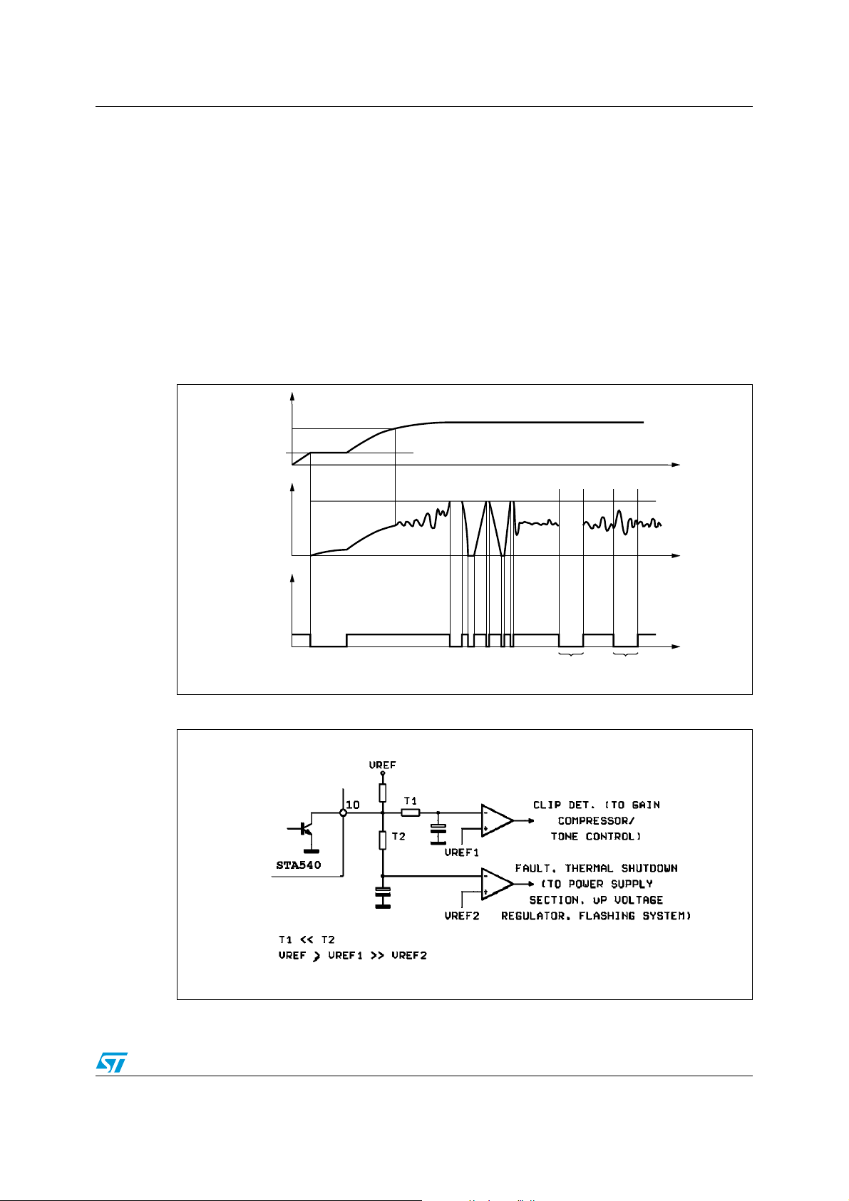
As different diagnostic information (clipping detection, output fault, approaching thermal
shutdown) becomes available at pin 10 so the behavior of the signal at this pin changes.
In order to discriminate the event, signal DIAGNOSTICD, pin 10, must be interpreted
correctly. Figure 27 shows a combination of events on the output waveform and the
corresponding output on pin 10.
This events could be diagnosed based on the timing of the output signal on pin 10. For
example, the clip-detector signalling under fault conditions could produce a low level for a
short time. On the other hand, an output short circuit would probably produce a low level for
a much longer time. With these assumptions, an interface circuit based on the one shown in
Figure 28 could differentiate the information and flag the appropriate circuits.
Figure 27. Waveforms
ST-BY PIN
VOLTAGE
t
Vs
OUTPUT
WAVEFORM
Vpin 10
WAVEFORM
D05AU1604mod
Figure 28. Interface circuit diagram
CLIPPING
SHORT TO GND
OR TO Vs
THERMAL
PROXIMITY
t
t
Doc ID 13907 Rev 6 21/25
Page 22
Practical information STA540
6.9 PCB ground layout
The device has two distinct ground pins, P-GND (power ground) and S-GND (signal ground)
which are disconnected from each other at chip level. For superior performance the pins
P-GND and S-GND must be connected together on the PCB by low-resistance tracks.
For the PCB-ground configuration, a star-like arrangement, where the center is represented
by the supply-filtering electrolytic capacitor ground, is recommended. In an arrangement
such as this, at least two separate paths must be provided, one for P-GND and one for
S-GND.
The correct ground assignments are as follows:
● on S-GND:
– standby capacitor (pin 7, or any other standby driving networks),
– SVR capacitor (pin 6), to be placed as close as possible to the device,
– input signal ground (from active/passive signal processor stages)
● on P-GND:
– power supply filtering capacitors for pins 3 and 13. The negative terminal of the
electrolytic capacitor(s) must be directly tied to the battery negative line and this
should represent the starting point for all the ground paths.
6.10 Mute function
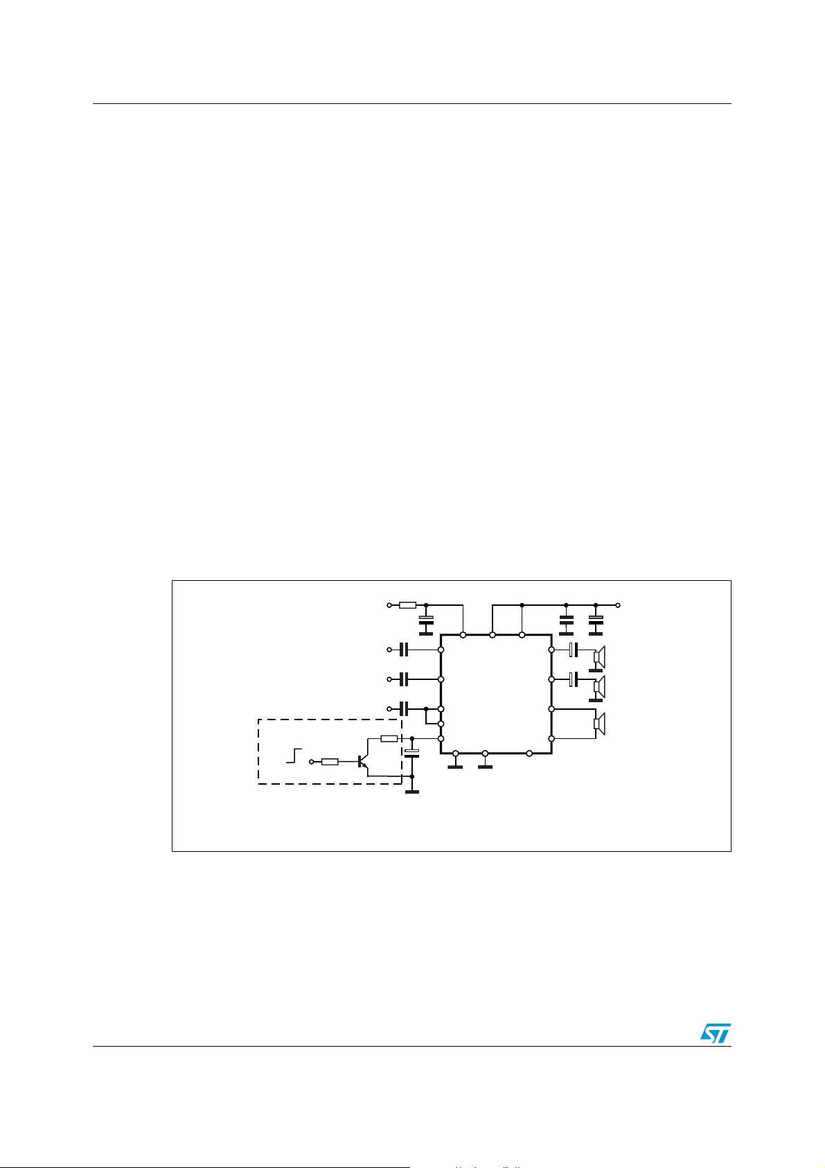
If the mute function is desired, it can be implemented on pin 6, SVR, as shown in Figure 29.
Figure 29. Optional mute function circuit
MUTE
0
PLAY
VS = 10 to 16 V,
mute off: V
mute on: V
Using a different value for R1 than the suggested 3.3 kΩ, results in two different situations:
● R1 > 3.3 kΩ:
– pop noise improvement,
– lower mute attenuation;
● R1 < 3.3 kΩ:
– pop noise degradation,
– higher mute attenuation.
≥ 0.6 to 0.8 V,
SVR
≥ 0.2 V
SVR
IN L
R1 3.3K
10K
0.22μF
0.22μF
0.47μF
470μF
10μF
13
7
4
5
11
6
8
9
DIAGNOSTICS
3
1
2200μF
2
2200μF
15
14
10
D06AU1632
ST-BY
IN R
IN BRIDGE 12
5V
R2 10K
1000μF100nF
OUT L
OUT R
OUT
BRIDGE
V
S
22/25 Doc ID 13907 Rev 6
Page 23
STA540 Package information
7 Package information
In order to meet environmental requirements, ST offers these devices in different grades of
ECOPACK
specifications, grade definitions and product status are available at: www.st.com.
ECOPACK
®
packages, depending on their level of environmental compliance. ECOPACK®
®
is an ST trademark.
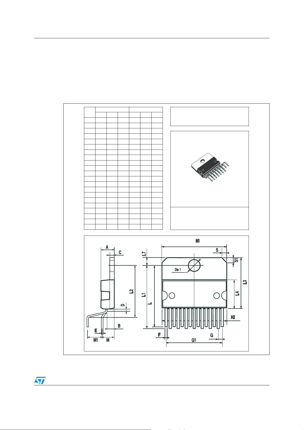
Figure 30. Mechanical data and package dimensions (Multiwatt15)
DIM.
A0.197
B 2.65 0.104
C 1.6 0.063
D1 0.039
E 0.49 0.55 0.019 0.022
F 0.66 0.75 0.026 0.030
G 1.02 1.27 1.52 0.040 0.050 0.060
G1 17.53 17.78 18.03 0.690 0.700 0.710
H1 19.6 0.772
H2 20.2 0.795
L 21.9 22.2 22.5 0.862 0.874 0.886
L1 21.7 22.1 22.5 0.854 0.870.886
L2 17.65 18.1 0.695 0.713
L3 17.25 17.5 17.7 5 0.679 0.689 0.699
L4 10.3 10.7 10.9 0.406 0.421 0.429
L7 2.65 2.9 0.104 0.114
M 4.25 4.55 4.85 0.167 0.179 0.191
M1 4.73 5.08 5.43 0.186 0.200 0.214
S 1.9 2.6 0.075 0.102
S1 1.9 2.6 0.075 0.102
Dia1 3.65 3.85 0.144 0.152
mm inch
MIN. TYP. MAX. MIN. TYP. MAX.
5
OUTLINE AND
MECHANICAL DATA
Multiwatt15 (Vertical)
0016036 J
Doc ID 13907 Rev 6 23/25
Page 24
Revision history STA540
8 Revision history
Table 6. Document revision history
Date Revision Changes
May-2006 1 Initial release
Sep-2006 2 Minor non-technical edits
Updated description on page 1
Oct-2007 3
Updated pin naming, numbering in all relevant figures
Minor non-technical edits
21-Jan-2008 4
02-Apr-2012 5
24-Apr-2012 6
Updated power specifications on pages 1, 6 and 8
Updated short-circuit output current in Table 5
Modified V
to VSB and updated parameters in Table 5: Electrical
ST-BY
characteristics
®
Updated ECOPACK
text in Section 7: Package information
Updated dimension A in Figure 30: Mechanical data and package
dimensions (Multiwatt15)
24/25 Doc ID 13907 Rev 6
Page 25

STA540
Please Read Carefully:
Information in this document is provided solely in connection with ST products. STMicroelectronics NV and its subsidiaries (“ST”) reserve the
right to make changes, corrections, modifications or improvements, to this document, and the products and services described herein at any
time, without notice.
All ST products are sold pursuant to ST’s terms and conditions of sale.
Purchasers are solely responsible for the choice, selection and use of the ST products and services described herein, and ST assumes no
liability whatsoever relating to the choice, selection or use of the ST products and services described herein.
No license, express or implied, by estoppel or otherwise, to any intellectual property rights is granted under this document. If any part of this
document refers to any third party products or services it shall not be deemed a license grant by ST for the use of such third party products
or services, or any intellectual property contained therein or considered as a warranty covering the use in any manner whatsoever of such
third party products or services or any intellectual property contained therein.
UNLESS OTHERWISE SET FORTH IN ST’S TERMS AND CONDITIONS OF SALE ST DISCLAIMS ANY EXPRESS OR IMPLIED
WARRANTY WITH RESPECT TO THE USE AND/OR SALE OF ST PRODUCTS INCLUDING WITHOUT LIMITATION IMPLIED
WARRANTIES OF MERCHANTABILITY, FITNESS FOR A PARTICULAR PURPOSE (AND THEIR EQUIVALENTS UNDER THE LAWS
OF ANY JURISDICTION), OR INFRINGEMENT OF ANY PATENT, COPYRIGHT OR OTHER INTELLECTUAL PROPERTY RIGHT.
UNLESS EXPRESSLY APPROVED IN WRITING BY TWO AUTHORIZED ST REPRESENTATIVES, ST PRODUCTS ARE NOT
RECOMMENDED, AUTHORIZED OR WARRANTED FOR USE IN MILITARY, AIR CRAFT, SPACE, LIFE SAVING, OR LIFE SUSTAINING
APPLICATIONS, NOR IN PRODUCTS OR SYSTEMS WHERE FAILURE OR MALFUNCTION MAY RESULT IN PERSONAL INJURY,
DEATH, OR SEVERE PROPERTY OR ENVIRONMENTAL DAMAGE. ST PRODUCTS WHICH ARE NOT SPECIFIED AS "AUTOMOTIVE
GRADE" MAY ONLY BE USED IN AUTOMOTIVE APPLICATIONS AT USER’S OWN RISK.
Resale of ST products with provisions different from the statements and/or technical features set forth in this document shall immediately void
any warranty granted by ST for the ST product or service described herein and shall not create or extend in any manner whatsoever, any
liability of ST.
ST and the ST logo are trademarks or registered trademarks of ST in various countries.
Information in this document supersedes and replaces all information previously supplied.
The ST logo is a registered trademark of STMicroelectronics. All other names are the property of their respective owners.
© 2012 STMicroelectronics - All rights reserved
STMicroelectronics group of companies
Australia - Belgium - Brazil - Canada - China - Czech Republic - Finland - France - Germany - Hong Kong - India - Israel - Italy - Japan -
Malaysia - Malta - Morocco - Philippines - Singapore - Spain - Sweden - Switzerland - United Kingdom - United States of America
www.st.com
Doc ID 13907 Rev 6 25/25
 Loading...