

Page 1
FFX™ audio codec with analog and digital inputs
and 2 x 1.2 W (or 2 x 100 mW HP) class-D amplifier
Features
■ Up to 96 dB dynamic range
■ Sample rates from 8 kHz to 192 kHz
■ FFX
■ 1.55 V to 1.95 V digital power supply
■ 1.80 V to 3.60 V analog and I/O power supply
■ 18-bit audio processing and class-D FFX
■ >90-dB SNR analog-to-digital converter
■ Digital volume control:
■ 16-bit ADC
■ Individual channel and master gain/attenuation
■ Automatic invalid input detect mute
■ 2-channel I
■ Digitally controlled pop-free operation
■ 90% efficiency
■ Output power for stereo headphones or stereo
Table 1. Device summary
™
class-D driver
modulator
– +36 dB to -105 dB in 0.5-dB steps
– Software volume update
2
S input/output data interface
speakers applications (at THD = 10% and
V
= 3.3 V):
CC
– 45 mW with 32-Ω headphones
– 85 mW with 16-Ω headphones
– 720 mW with 8-Ω speakers
– 1.1 W with 4-Ω speakers
™
STA529
Datasheet − production data
TFBGA48
VFQFPN52
Applications
■ Portable devices
– Laptops
– Digital cameras
– Microless applications
Order code Operating temp. range Package Packaging
STA529Q -40 to 85 °C VFQFPN52 Tray
STA529 -40 to 85 °C TFBGA48 Tray
March 2012 Doc ID 13095 Rev 3 1/57
This is information on a product in full production.
www.st.com
57
Page 2

Contents STA529
Contents
1 Description . . . . . . . . . . . . . . . . . . . . . . . . . . . . . . . . . . . . . . . . . . . . . . . . . 7
2 Connection diagrams and pin descriptions . . . . . . . . . . . . . . . . . . . . . . 8
2.1 TFBGA48 package . . . . . . . . . . . . . . . . . . . . . . . . . . . . . . . . . . . . . . . . . . . 8
2.2 VFQFPN52 package . . . . . . . . . . . . . . . . . . . . . . . . . . . . . . . . . . . . . . . . 10
3 Electrical and thermal specifications . . . . . . . . . . . . . . . . . . . . . . . . . . 13
3.1 Thermal data . . . . . . . . . . . . . . . . . . . . . . . . . . . . . . . . . . . . . . . . . . . . . . 13
3.2 Absolute maximum ratings . . . . . . . . . . . . . . . . . . . . . . . . . . . . . . . . . . . . 13
3.3 Recommended operating conditions . . . . . . . . . . . . . . . . . . . . . . . . . . . . 14
3.4 Electrical characteristics . . . . . . . . . . . . . . . . . . . . . . . . . . . . . . . . . . . . . . 15
3.5 Lock time . . . . . . . . . . . . . . . . . . . . . . . . . . . . . . . . . . . . . . . . . . . . . . . . . 16
4 Input clock . . . . . . . . . . . . . . . . . . . . . . . . . . . . . . . . . . . . . . . . . . . . . . . . 17
4.1 SELCLK33 . . . . . . . . . . . . . . . . . . . . . . . . . . . . . . . . . . . . . . . . . . . . . . . . 17
5 Digital processing . . . . . . . . . . . . . . . . . . . . . . . . . . . . . . . . . . . . . . . . . . 18
5.1 Signal processing flow . . . . . . . . . . . . . . . . . . . . . . . . . . . . . . . . . . . . . . . 18
5.2 I
5.3 Volume control and gain . . . . . . . . . . . . . . . . . . . . . . . . . . . . . . . . . . . . . . 19
2
C interface disable . . . . . . . . . . . . . . . . . . . . . . . . . . . . . . . . . . . . . . . . 18
6 PLL . . . . . . . . . . . . . . . . . . . . . . . . . . . . . . . . . . . . . . . . . . . . . . . . . . . . . . 20
6.1 Functional description . . . . . . . . . . . . . . . . . . . . . . . . . . . . . . . . . . . . . . . 20
6.2 Configuration examples . . . . . . . . . . . . . . . . . . . . . . . . . . . . . . . . . . . . . . 22
6.3 Set fractional PLL . . . . . . . . . . . . . . . . . . . . . . . . . . . . . . . . . . . . . . . . . . . 24
7 ADC . . . . . . . . . . . . . . . . . . . . . . . . . . . . . . . . . . . . . . . . . . . . . . . . . . . . . . 25
7.1 ADC performance values . . . . . . . . . . . . . . . . . . . . . . . . . . . . . . . . . . . . . 25
7.2 Functional description . . . . . . . . . . . . . . . . . . . . . . . . . . . . . . . . . . . . . . . 25
7.2.1 Digital filter characteristics . . . . . . . . . . . . . . . . . . . . . . . . . . . . . . . . . . . 26
7.2.2 High-pass filter characteristics . . . . . . . . . . . . . . . . . . . . . . . . . . . . . . . . 26
7.2.3 Programmable gain amplifier (PGA) . . . . . . . . . . . . . . . . . . . . . . . . . . . 26
7.3 Applications scheme . . . . . . . . . . . . . . . . . . . . . . . . . . . . . . . . . . . . . . . . 27
2/57 Doc ID 13095 Rev 3
Page 3

STA529 Contents
7.4 Configuration examples . . . . . . . . . . . . . . . . . . . . . . . . . . . . . . . . . . . . . . 27
8 Driver configuration . . . . . . . . . . . . . . . . . . . . . . . . . . . . . . . . . . . . . . . . 28
8.1 I2S bypass . . . . . . . . . . . . . . . . . . . . . . . . . . . . . . . . . . . . . . . . . . . . . . . . 28
9 Serial audio interface . . . . . . . . . . . . . . . . . . . . . . . . . . . . . . . . . . . . . . . 29
9.1 Master mode . . . . . . . . . . . . . . . . . . . . . . . . . . . . . . . . . . . . . . . . . . . . . . 29
9.2 Slave mode . . . . . . . . . . . . . . . . . . . . . . . . . . . . . . . . . . . . . . . . . . . . . . . 30
9.3 Serial formats . . . . . . . . . . . . . . . . . . . . . . . . . . . . . . . . . . . . . . . . . . . . . . 31
9.3.1 DSP . . . . . . . . . . . . . . . . . . . . . . . . . . . . . . . . . . . . . . . . . . . . . . . . . . . . 32
9.3.2 I
9.3.3 PCM/IF (non-delayed mode) . . . . . . . . . . . . . . . . . . . . . . . . . . . . . . . . . 33
9.3.4 PCM/IF (delayed mode) . . . . . . . . . . . . . . . . . . . . . . . . . . . . . . . . . . . . . 33
2
S . . . . . . . . . . . . . . . . . . . . . . . . . . . . . . . . . . . . . . . . . . . . . . . . . . . . . 32
10 I2C interface . . . . . . . . . . . . . . . . . . . . . . . . . . . . . . . . . . . . . . . . . . . . . . . 34
10.1 Data transition and change . . . . . . . . . . . . . . . . . . . . . . . . . . . . . . . . . . . 34
10.2 Start condition . . . . . . . . . . . . . . . . . . . . . . . . . . . . . . . . . . . . . . . . . . . . . 34
10.3 Stop condition . . . . . . . . . . . . . . . . . . . . . . . . . . . . . . . . . . . . . . . . . . . . . 34
10.4 Data input . . . . . . . . . . . . . . . . . . . . . . . . . . . . . . . . . . . . . . . . . . . . . . . . . 34
10.5 Device addressing . . . . . . . . . . . . . . . . . . . . . . . . . . . . . . . . . . . . . . . . . . 34
10.6 Write operation . . . . . . . . . . . . . . . . . . . . . . . . . . . . . . . . . . . . . . . . . . . . . 35
10.6.1 Byte write . . . . . . . . . . . . . . . . . . . . . . . . . . . . . . . . . . . . . . . . . . . . . . . . 35
10.6.2 Multi-byte write . . . . . . . . . . . . . . . . . . . . . . . . . . . . . . . . . . . . . . . . . . . . 35
10.7 Read operation . . . . . . . . . . . . . . . . . . . . . . . . . . . . . . . . . . . . . . . . . . . . . 35
10.7.1 Current address byte read . . . . . . . . . . . . . . . . . . . . . . . . . . . . . . . . . . . 35
10.7.2 Current address multi-byte read . . . . . . . . . . . . . . . . . . . . . . . . . . . . . . 35
10.7.3 Random address byte read . . . . . . . . . . . . . . . . . . . . . . . . . . . . . . . . . . 35
10.7.4 Random address multi-byte read . . . . . . . . . . . . . . . . . . . . . . . . . . . . . . 36
11 Registers . . . . . . . . . . . . . . . . . . . . . . . . . . . . . . . . . . . . . . . . . . . . . . . . . 37
11.1 Summary . . . . . . . . . . . . . . . . . . . . . . . . . . . . . . . . . . . . . . . . . . . . . . . . . 37
11.2 General registers . . . . . . . . . . . . . . . . . . . . . . . . . . . . . . . . . . . . . . . . . . . 38
12 Package mechanical data . . . . . . . . . . . . . . . . . . . . . . . . . . . . . . . . . . . . 53
12.1 Package TFBGA48 . . . . . . . . . . . . . . . . . . . . . . . . . . . . . . . . . . . . . . . . . . 53
12.2 Package VFQFPN52 . . . . . . . . . . . . . . . . . . . . . . . . . . . . . . . . . . . . . . . . 55
Doc ID 13095 Rev 3 3/57
Page 4

Contents STA529
13 Revision history . . . . . . . . . . . . . . . . . . . . . . . . . . . . . . . . . . . . . . . . . . . 56
4/57 Doc ID 13095 Rev 3
Page 5

STA529 List of figures
List of figures
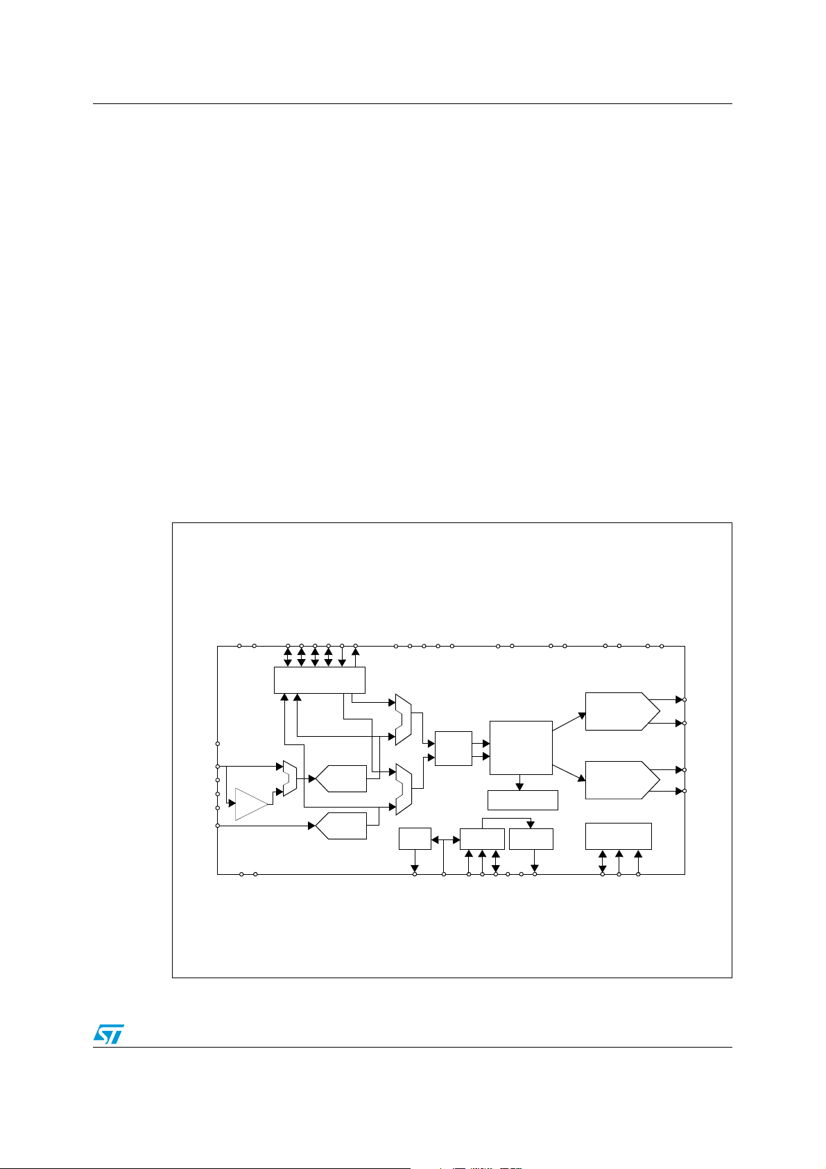
Figure 1. Block diagram . . . . . . . . . . . . . . . . . . . . . . . . . . . . . . . . . . . . . . . . . . . . . . . . . . . . . . . . . . . 7
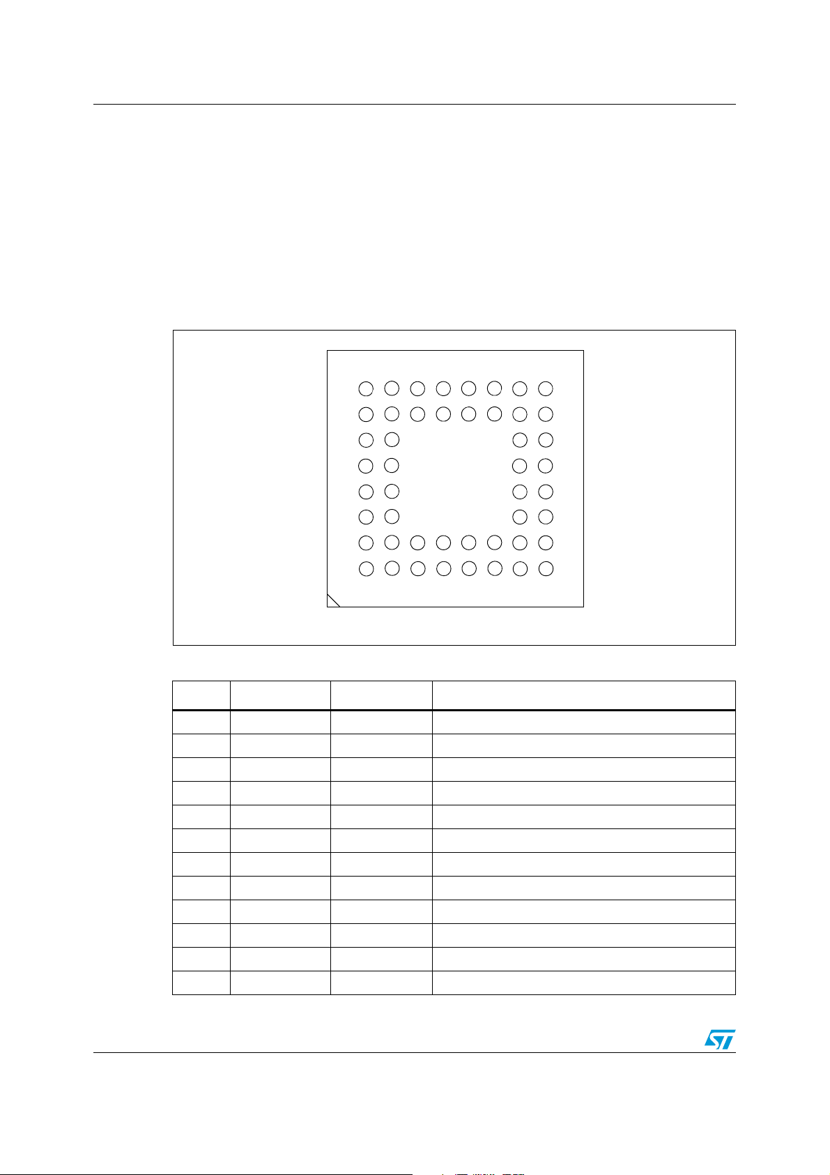
Figure 2. Connection diagram for TFBGA48 (bottom view) . . . . . . . . . . . . . . . . . . . . . . . . . . . . . . . . 8
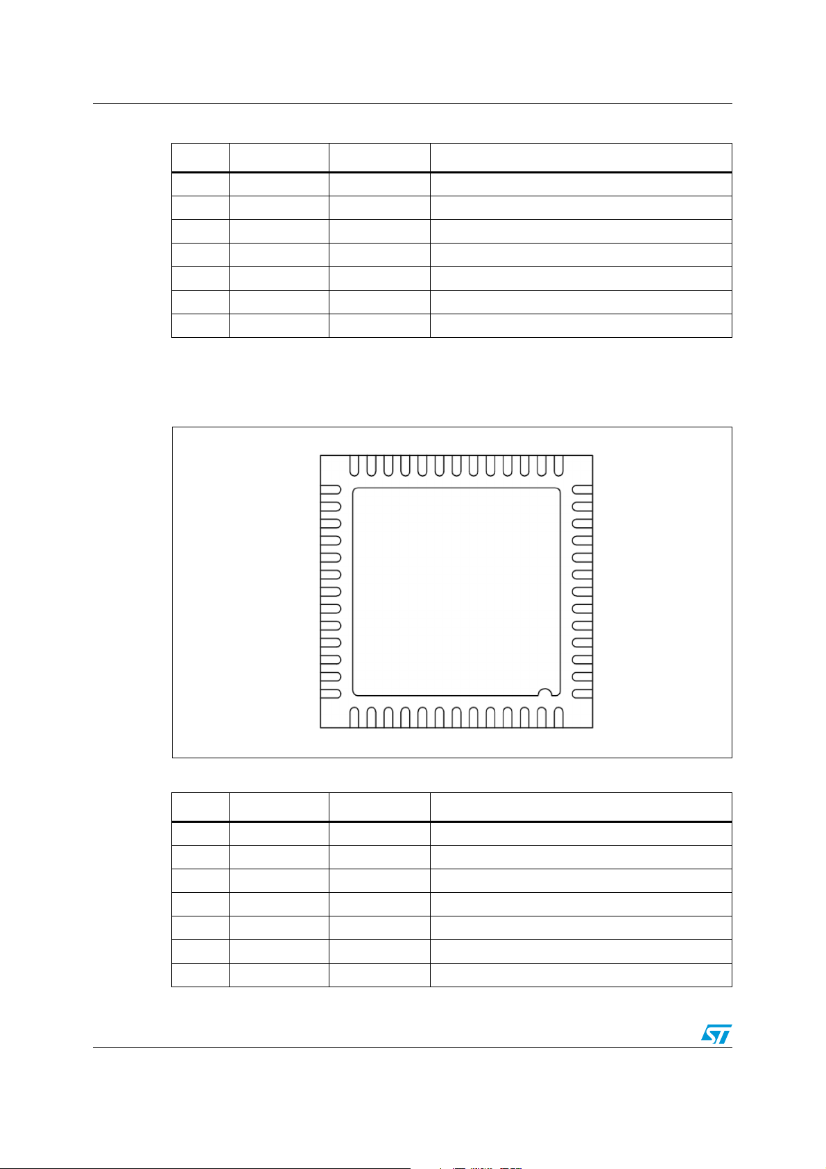
Figure 3. Connection diagram for VFQFPN52 (bottom view) . . . . . . . . . . . . . . . . . . . . . . . . . . . . . . 10
Figure 4. Circuit for crystal drive . . . . . . . . . . . . . . . . . . . . . . . . . . . . . . . . . . . . . . . . . . . . . . . . . . . . 17
Figure 5. PLL block diagram . . . . . . . . . . . . . . . . . . . . . . . . . . . . . . . . . . . . . . . . . . . . . . . . . . . . . . . 20
Figure 6. PLL filter circuit . . . . . . . . . . . . . . . . . . . . . . . . . . . . . . . . . . . . . . . . . . . . . . . . . . . . . . . . . 21
Figure 7. Diagram of input coupling and supply decoupling . . . . . . . . . . . . . . . . . . . . . . . . . . . . . . . 27
Figure 8. Master mode . . . . . . . . . . . . . . . . . . . . . . . . . . . . . . . . . . . . . . . . . . . . . . . . . . . . . . . . . . . . 29
Figure 9. Slave mode . . . . . . . . . . . . . . . . . . . . . . . . . . . . . . . . . . . . . . . . . . . . . . . . . . . . . . . . . . . . 30
Figure 10. Right justified . . . . . . . . . . . . . . . . . . . . . . . . . . . . . . . . . . . . . . . . . . . . . . . . . . . . . . . . . . . 31
Figure 11. Left justified. . . . . . . . . . . . . . . . . . . . . . . . . . . . . . . . . . . . . . . . . . . . . . . . . . . . . . . . . . . . . 31
Figure 12. DSP . . . . . . . . . . . . . . . . . . . . . . . . . . . . . . . . . . . . . . . . . . . . . . . . . . . . . . . . . . . . . . . . . . 32
Figure 13. I
Figure 14. PCM/IF (non delayed mode). . . . . . . . . . . . . . . . . . . . . . . . . . . . . . . . . . . . . . . . . . . . . . . . 33
Figure 15. PCM/IF (delayed mode) . . . . . . . . . . . . . . . . . . . . . . . . . . . . . . . . . . . . . . . . . . . . . . . . . . . 33
Figure 16. I
Figure 17. I
Figure 18. Package outline (TFBGA48) . . . . . . . . . . . . . . . . . . . . . . . . . . . . . . . . . . . . . . . . . . . . . . . 53
Figure 19. Package outline (VFQFPN52) . . . . . . . . . . . . . . . . . . . . . . . . . . . . . . . . . . . . . . . . . . . . . . 55
2
S. . . . . . . . . . . . . . . . . . . . . . . . . . . . . . . . . . . . . . . . . . . . . . . . . . . . . . . . . . . . . . . . . . . . 32
2
C write operations . . . . . . . . . . . . . . . . . . . . . . . . . . . . . . . . . . . . . . . . . . . . . . . . . . . . . . 36
2
C read operations . . . . . . . . . . . . . . . . . . . . . . . . . . . . . . . . . . . . . . . . . . . . . . . . . . . . . . 36
Doc ID 13095 Rev 3 5/57
Page 6

List of tables STA529
List of tables
Table 1. Device summary . . . . . . . . . . . . . . . . . . . . . . . . . . . . . . . . . . . . . . . . . . . . . . . . . . . . . . . . . . 1
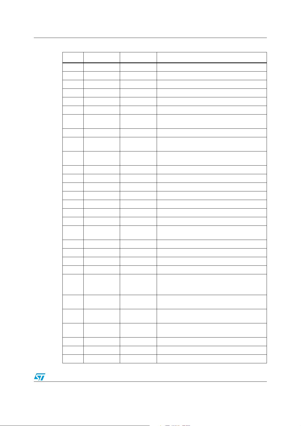
Table 2. Pin description for TFBGA48 . . . . . . . . . . . . . . . . . . . . . . . . . . . . . . . . . . . . . . . . . . . . . . . . 8
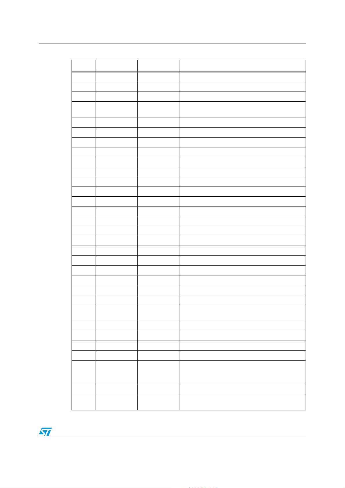
Table 3. Pin description for VFQFPN52 . . . . . . . . . . . . . . . . . . . . . . . . . . . . . . . . . . . . . . . . . . . . . . 10
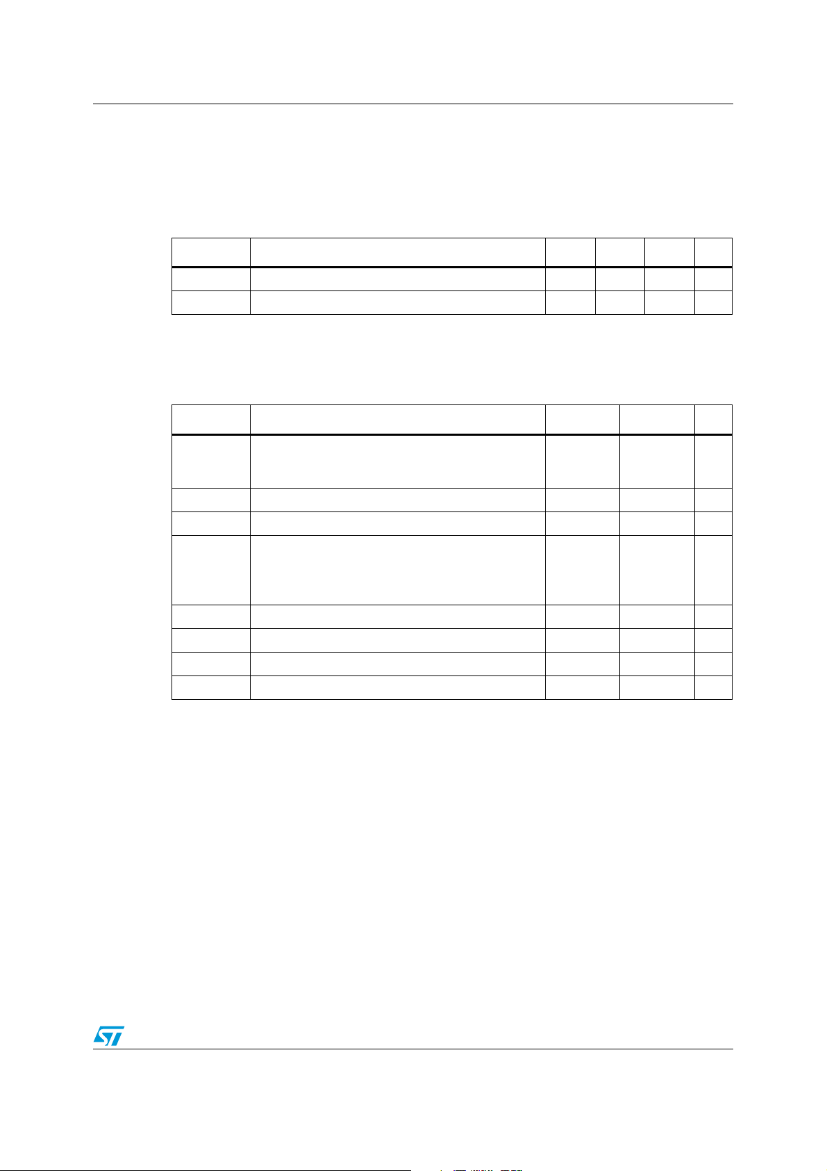
Table 4. Thermal data. . . . . . . . . . . . . . . . . . . . . . . . . . . . . . . . . . . . . . . . . . . . . . . . . . . . . . . . . . . . 13
Table 5. Absolute maximum ratings . . . . . . . . . . . . . . . . . . . . . . . . . . . . . . . . . . . . . . . . . . . . . . . . . 13
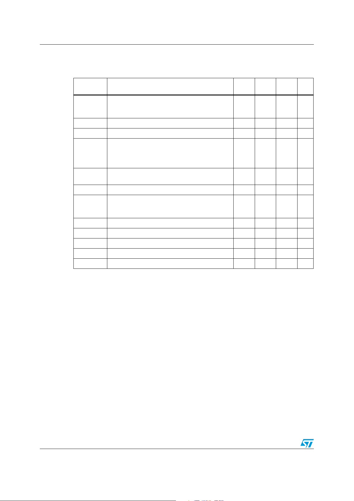
Table 6. Recommended operating conditions . . . . . . . . . . . . . . . . . . . . . . . . . . . . . . . . . . . . . . . . . 14
Table 7. Electrical characteristics . . . . . . . . . . . . . . . . . . . . . . . . . . . . . . . . . . . . . . . . . . . . . . . . . . . 15
Table 8. Load power at 1% distortion in headphone mode . . . . . . . . . . . . . . . . . . . . . . . . . . . . . . . 16
Table 9. Load power at 10% distortion in headphone mode . . . . . . . . . . . . . . . . . . . . . . . . . . . . . . 16
Table 10. Load power at 1% distortion in speaker mode . . . . . . . . . . . . . . . . . . . . . . . . . . . . . . . . . . 16
Table 11. Load power at 10% distortion in speaker mode . . . . . . . . . . . . . . . . . . . . . . . . . . . . . . . . . 16
Table 12. PLL lock time . . . . . . . . . . . . . . . . . . . . . . . . . . . . . . . . . . . . . . . . . . . . . . . . . . . . . . . . . . . 16
Table 13. Master volume offset as a function of register MVOL . . . . . . . . . . . . . . . . . . . . . . . . . . . . . 19
Table 14. Channel volume as a function of registers LVOL and RVOL . . . . . . . . . . . . . . . . . . . . . . . 19
Table 15. Oversampling table . . . . . . . . . . . . . . . . . . . . . . . . . . . . . . . . . . . . . . . . . . . . . . . . . . . . . . . 23
Table 16. Programmable gain performance . . . . . . . . . . . . . . . . . . . . . . . . . . . . . . . . . . . . . . . . . . . . 25
Table 17. Digital filter characteristics . . . . . . . . . . . . . . . . . . . . . . . . . . . . . . . . . . . . . . . . . . . . . . . . . 26
Table 18. High-pass filter characteristics . . . . . . . . . . . . . . . . . . . . . . . . . . . . . . . . . . . . . . . . . . . . . . 26
Table 19. Pin functions in driver-configuration mode . . . . . . . . . . . . . . . . . . . . . . . . . . . . . . . . . . . . . 28
Table 20. Master mode . . . . . . . . . . . . . . . . . . . . . . . . . . . . . . . . . . . . . . . . . . . . . . . . . . . . . . . . . . . . 29
Table 21. Slave mode . . . . . . . . . . . . . . . . . . . . . . . . . . . . . . . . . . . . . . . . . . . . . . . . . . . . . . . . . . . . . 30
Table 22. Register summary. . . . . . . . . . . . . . . . . . . . . . . . . . . . . . . . . . . . . . . . . . . . . . . . . . . . . . . . 37
Table 23. Package dimensions (TFBGA48) . . . . . . . . . . . . . . . . . . . . . . . . . . . . . . . . . . . . . . . . . . . . 54
Table 24. Package dimensions (VFQFPN52). . . . . . . . . . . . . . . . . . . . . . . . . . . . . . . . . . . . . . . . . . . 55
Table 25. Document revision history . . . . . . . . . . . . . . . . . . . . . . . . . . . . . . . . . . . . . . . . . . . . . . . . . 56
6/57 Doc ID 13095 Rev 3
Page 7
STA529 Description
1 Description
The STA529 is a digital stereo class-D audio amplifier. It includes an audio DSP, an ST
proprietary high-efficiency class-D driver and CMOS power output stage. It is intended for
high-efficiency digital-to-power-audio conversion for portable applications. The STA529 also
provides output capabilities for FFX
provides high-quality digital amplification.
The STA529 contains an on-chip volume/gain control.
The PWM amplifier achieves greater than 90% efficiency for longer battery life for portable
systems.
The innovative class-D modulation, allows the STA529 to work without external LC filters
and without a heatsink.
The STA529 I2CDIS pin disables the audio DSP functions and the I
direct conversion of the input signal into output power. This conversion is done without the
microcontroller.
The STA529 is designed for low-power operation with extremely low-current consumption in
standby mode. It is available in packages TFBGA48 and VFQFPN52. These are very thin
packages (1.2 mm thick) ideal for small portable applications.
™
. In conjunction with a power device, the STA529
2
C interface provides a
Figure 1. Block diagram
BICLKO / PWM1A
LRCLKI
BICLKI
Serial digital
LRCLKO / PWM1B
ADC
ADC
VBIAS
INL
VHI
VCM
VLO
INR
VDD
PGA
AVC C
GND
audio interface
MUX
AGND
SDATAI
SDATAO / PWM2A
RST_NTMSTBY
MUX
MUX
XTO
MUTE
POWERFAULT / EADP
Digital
volume
XTI
MCLK33
SELCLK33
GNDIO
VDDIO
FFX
modulator
PWM out I/F
DividerPLLOSC
FILT
VDDPLL
GNDPLL
GND33
VCC33
GND2
GND1
Power
driver
Powe r
driver
Control
interface
SCL
SDA
VCC2
I2CDIS
VCC1
OUT1A
OUT1B
OUT2A
OUT2B
CLKOUT / PWM2B
Doc ID 13095 Rev 3 7/57
Page 8
Connection diagrams and pin descriptions STA529
2 Connection diagrams and pin descriptions
This section includes connection diagrams and pin descriptions for the following packages:
● TFBGA48
● VFQFPN52
2.1 TFBGA48 package
Figure 2. Connection diagram for TFBGA48 (bottom view)
H
G
F
E
D
C
B
A
12345678
Table 2. Pin description for TFBGA48
Pin Name Type Description
A1 VCC2 Supply Channel 2 power supply
A2 GND2 Ground Channel 2 power ground
A3 OUT2A Analog output Channel 2 half-bridge A output
A4 OUT2B Analog output Channel 2 half-bridge B output
A5 OUT1B Analog output Channel 1 half-bridge B output
A6 OUT1A Analog output Channel 1 half-bridge A output
A7 GND1 Ground Channel 1 power ground
A8 VCC1 Supply Channel 1 power supply
B1 GNDIO Ground I/O ring ground
B2 GND33 Ground Pre-driver ground
B3 OUT2A Analog output Channel 2 half-bridge A output
B4 OUT2B Analog output Channel 2 half-bridge B output
8/57 Doc ID 13095 Rev 3
Page 9
STA529 Connection diagrams and pin descriptions
Table 2. Pin description for TFBGA48 (continued)
Pin Name Type Description
B5 OUT1B Analog output Channel 1 half-bridge B output
B6 OUT1A Analog output Channel 1 half-bridge A output
B7 MUTE Digital input Mute (active high)
B8 GND Ground Digital ground
C1 VDDIO Supply I/O ring supply
C2 VCC33 Supply Pre-driver supply
C7
C8 VDD Supply Digital supply
D1 XTI
D2 XTO
D7 RST_N Digital input Reset (active low)
D8 VCM Analog I/O ADC common mode voltage
CLKOUT /
PWM2B
Digital output Buffered clock output / PWM2B FFX
Digital input
1.8V
Digital output
1.8V
Crystal input or master clock input
Crystal output
E1 MCLK33 Digital input Master clock input 3.3-V capable
E2 SDATAI Digital input Input serial audio interface data
E7 VLO Analog input ADC low reference voltage
E8 AGND Ground ADC analog ground
2
F1 SCL Digital input I
F2
POWERFAULT /
EAPD
Digital output
C serial clock
Power fault signal (active high) /
external audio power-down signal
F7 VHI Analog input ADC high reference voltage
F8 AVDD Supply ADC analog supply
2
G1 SDA Digital I/O I
G2 I2CDIS Digital input I
C serial data
2
C disable pin (active high)
Master clock input selector:
G3 SELCLK33 Digital input
0: XTI selected
1: MCLK33 selected
G4
G5
G6
SDATAO /
PWM2A
LRCLKO /
PWM1B
BICLKO /
PWM1A
Digital output Output serial audio interface data / PWM2A FFX
Digital I/O
Digital I/O
Output serial audio interface L/R-clock
(volume increases when I2CDIS = 1) / PWM1B FFX
Output serial audio interface bit-clock
(volume decreases when I2CDIS = 1) / PWM1A FFX
G7 VBIAS Analog I/O ADC microphone bias voltage
G8 STBY Digital input Standby (active high)
H1 FILT Analog I/O PLL loop filter terminal
Doc ID 13095 Rev 3 9/57
Page 10
Connection diagrams and pin descriptions STA529
Table 2. Pin description for TFBGA48 (continued)
Pin Name Type Description
H2 TM Digital input Test mode (active high)
H3 GNDPLL Ground PLL analog ground
H4 VDDPLL Supply PLL analog supply
H5 LRCLKI Digital I/O Input serial audio interface L/R-clock
H6 BICLKI Digital I/O Input serial audio interface bit-clock
H7 INL Analog input ADC left channel line input or microphone input
H8 INR Analog I/O ADC right channel line input
2.2 VFQFPN52 package
Figure 3. Connection diagram for VFQFPN52 (bottom view)
27
26
14
13
Table 3. Pin description for VFQFPN52
39
40
52
1
Pin Name Type Description
1 STBY Digital input Standby (active high)
2 INL Analog input ADC left channel line input or microphone input
3 INR Analog I/O ADC right channel line input
4 VBIAS Analog I/O ADC microphone bias voltage
5 AVDD Supply ADC analog supply
6 VHI Analog input ADC high reference voltage
7 VLO Analog input ADC low reference voltage
10/57 Doc ID 13095 Rev 3
Page 11
STA529 Connection diagrams and pin descriptions
Table 3. Pin description for VFQFPN52 (continued)
Pin Name Type Description
8 AGND Ground ADC analog ground
9 VCM Analog I/O ADC Common mode voltage
10 RST_N Digital input Reset (active low)
11
12 GND1 Ground Digital ground
13 VDD1 Supply Digital supply
14 MUTE Digital input Mute (active high)
15 VCC1A Supply Channel 1 half-bridge A power supply
16 OUT1A Analog output Channel 1 half-bridge A output
17 GND1A Ground Channel 1 half-bridge A power ground
18 GND1B Ground Channel 1 half-bridge B power ground
19 OUT1B Analog output Channel 1 half-bridge B output
20 VCC1B Supply Channel 1 half-bridge B power supply
21 VCC2B Supply Channel 2 half-bridge B power supply
CLKOUT /
PWM2B
Digital output Buffered clock output / PWM2B FFX
22 OUT2B Analog output Channel 2 half-bridge B output
23 GND2B Ground Channel 2 half-bridge B power ground
24 GND2A Ground Channel 2 half-bridge A power ground
25 OUT2A Analog output Channel 2 half-bridge A output
26 VCC2A Supply Channel 2 half-bridge A power supply
27 GND33 Ground Pre-driver ground
28 GNDIO1 Ground I/O ring ground
29 VDDIO1 Supply I/O ring supply
30 VCC33 Supply Pre-driver supply
31
POWERFAULT /
EAPD
Digital output
Power fault signal (active high) / external audio power
down signal
32 TM Digital input Test mode (active high)
2
33 I2CDIS Digital input I
34 SCL Digital input I
35 SDA Digital I/O I
C disable pin (active high)
2
C serial clock
2
C serial data
Master clock input selector:
36 SELCLK33 Digital input
0: XTI selected
1: MCLK33 selected
37 MCLK33 Digital input Master clock input 3.3-V capable
38 XTI
Digital input
1.8V
Crystal input or master clock input
Doc ID 13095 Rev 3 11/57
Page 12

Connection diagrams and pin descriptions STA529
Table 3. Pin description for VFQFPN52 (continued)
Pin Name Type Description
39 XTO
40 FILT Analog I/O PLL loop filter terminal
41 GNDPLL Ground PLL analog ground
42 VDDPLL Supply PLL analog supply
43 GND2 Ground Digital ground
44 VDD2 Supply Digital supply
45 SDATAI Digital input Input serial audio interface data
46
47 LRCLKI Digital I/O Input serial audio interface L/R-clock
48
49 GNDIO2 Ground I/O ring ground
50 VDDIO2 Supply I/O ring supply
51 BICLKI Digital I/O Input serial audio interface bit-clock
52
SDATAO /
PWM2A
LRCLKO /
PWM1B
BICLKO /
PWM1A
Digital output
1.8V
Digital output Output serial audio interface data / PWM2A FFX
Digital I/O
Digital I/O
Crystal output
Output serial audio interface L/R-clock
(volume increases when I2CDIS = 1) / PWM1B FFX
Output serial audio interface bit-clock
(volume decreases when I2CDIS = 1) / PWM1A FFX
12/57 Doc ID 13095 Rev 3
Page 13
STA529 Electrical and thermal specifications
3 Electrical and thermal specifications
3.1 Thermal data
Table 4. Thermal data
Device Parameter Min Typ Max Unit
TFBGA48 Thermal resistance junction to ambient - 40 - °C/W
VFQFPN52 Thermal resistance junction to ambient - 22 - °C/W
3.2 Absolute maximum ratings
Table 5. Absolute maximum ratings
Pin/symbol Description Min Max Unit
VDD
VDD1
VDD2
AVDD ADC supply voltage -0.5 +4 V
VDDPLL PLL analog supply voltage -0.5 +2.5 V
Digital supply voltage -0.5 +2.5 V
VCC1A
VCC1B
VCC2A
Power stage supply voltage -0.5 +4 V
VCC2B
VCC33 Pre-driver supply -0.5 +4 V
VDDIO Digital I/O supply -0.5 +4 V
T
T
STG
J
Storage temperature -40 150
Junction temperature -40 150
Note: All grounds must be within 0.3 V of each other.
o
C
o
C
Doc ID 13095 Rev 3 13/57
Page 14
Electrical and thermal specifications STA529
3.3 Recommended operating conditions
Table 6. Recommended operating conditions
Symbol Parameter Min Typ Max Unit
VDD
VDD1
VDD2
AVDD ADC supply voltage 1.8 3.3 3.6 V
VDDPLL PLL analog supply voltage 1.55 1.80 1.95 V
VCC1A
VCC1B
VCC2A
VCC2B
Digital supply voltage 1.55 1.80 1.95 V
Power stage supply voltage 1.8 3.0 3.3 V
VCC33
Pre-driver supply
(must be at same level as VCC1A/1B/2A/2B)
1.8 3.0 3.3 V
VDDIO Power supply for I/Os 1.8 3.0 3.6 V
GND1,
GND2,
Channel 1 and 2 power ground, pre-driver ground - 0 - V
GND33
GNDIO Ground for I/Os - 0 - V
IH 3.3-V supply 2.0 - - V
V
V
IL 3.3-V supply - - 0.8 V
HYST Schmitt trigger hysteresis (VDDIO) 0.4 - - V
V
T
AMB
Ambient operating temperature -40 - 85
o
C
14/57 Doc ID 13095 Rev 3
Page 15
STA529 Electrical and thermal specifications
3.4 Electrical characteristics
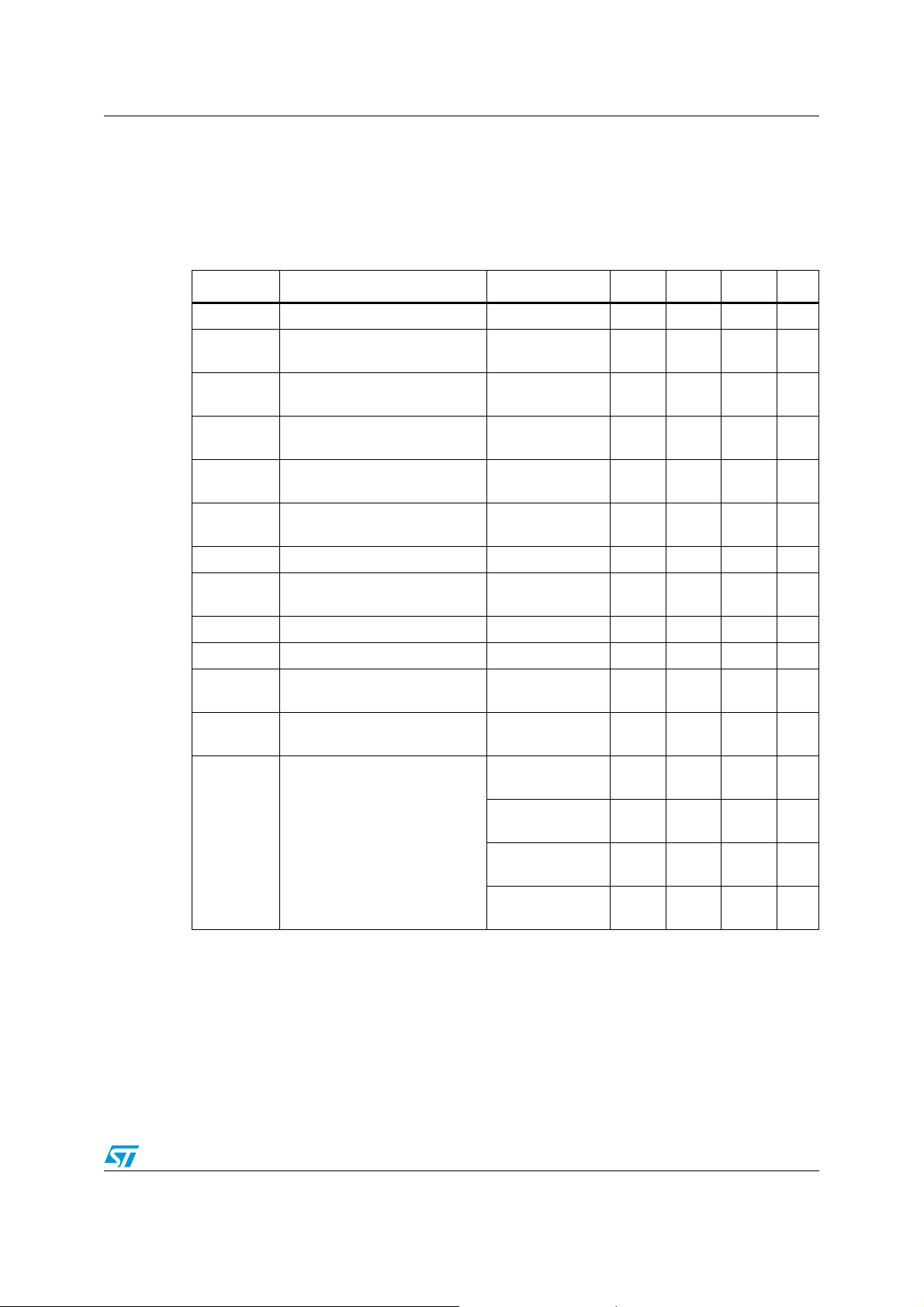
The electrical specifications in Ta bl e 7 below are given for operation under the
recommended conditions listed in Ta bl e 6 . Unless otherwise specified, LRCLKI frequency
(fs) = 48 kHz, input frequency = 1 kHz, and R
Table 7. Electrical characteristics
Symbol Parameter Test conditions Min Typ Max Unit
Eff Output power efficiency - - 90 - %
R
dson
Output stage N/PMOS onresistance
= 32 Ω.
LOAD
- - 250 380 mΩ
IstbyL
IstbyP
IddL
IddP
Tds Low current dead time (static) - - 1 - ns
Tdd
Tr Rise time - - 3 - ns
Tf Fall time - - 3 - ns
DNR
SNR
THDN Total harmonic distortion
Logic power supply current at
standby
Bridges power supply current in
standby
Logic power supply current at
operating
Bridges power supply current at
operating
High current dead time
(dynamic)
Dynamic range
A-weighted
Signal-to-noise ratio (Aweighted)
--1.3-µA
--0.7-µA
--15-mA
--0.5-mA
--2.5-ns
Speaker mode - 96 - dB
Speaker mode - 92 - dB
0 dBFS input,
8 Ω speakers
-6 dBFS input,
8 Ω speakers
0 dBFS input,
32 Ω headphones
-0.1-%
-0.05-%
-0.1-%
-6 dBFS input,
32 Ω headphones
Doc ID 13095 Rev 3 15/57
-0.05-%
Page 16
Electrical and thermal specifications STA529
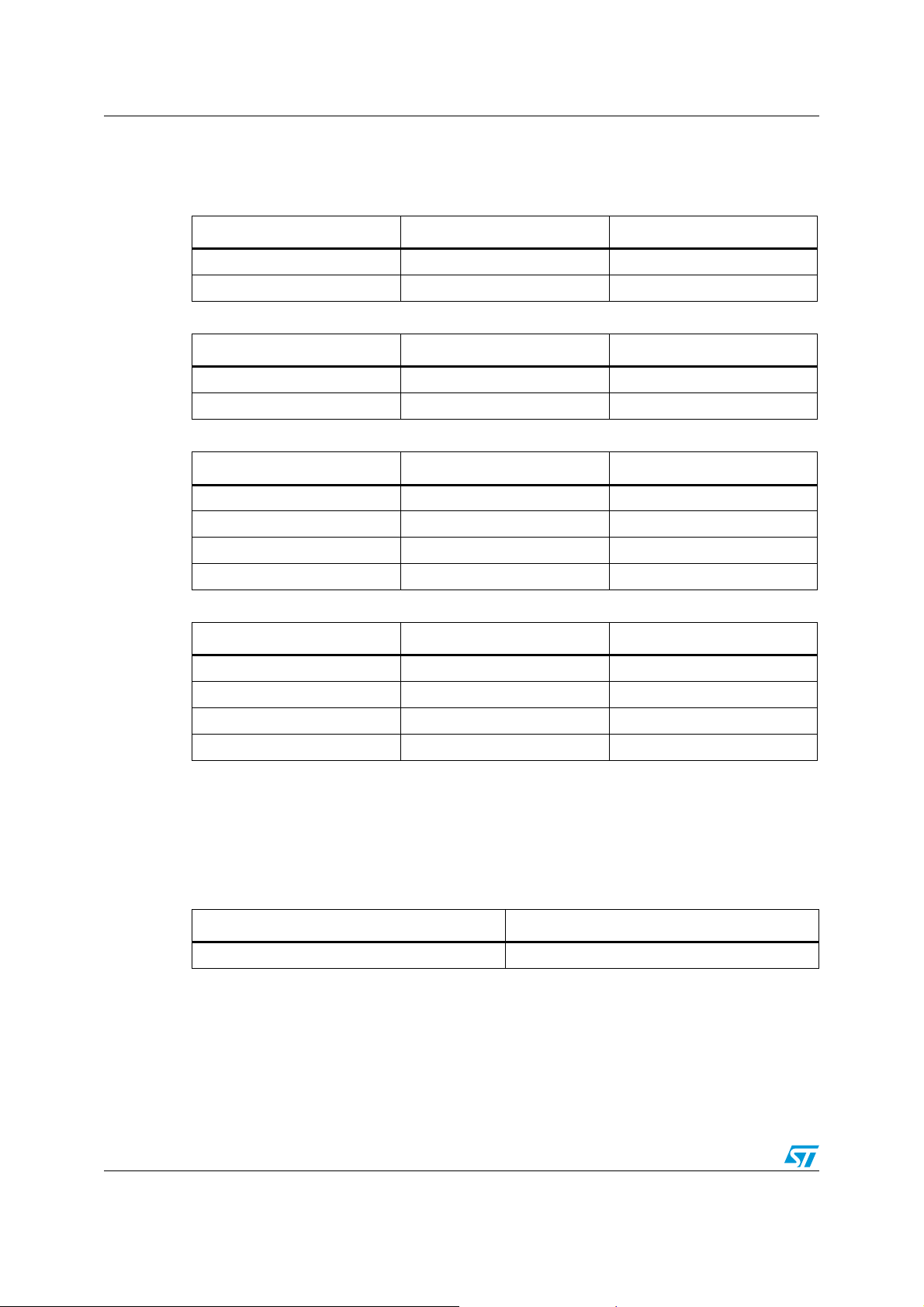
The following tables give the output power for 1% and 10% THD levels for headphones and
speakers.
Table 8. Load power at 1% distortion in headphone mode
Load (Ω) P (mW) at 1.8 V P (mW) at 3.3 V
16 20 65
32 10 32
Table 9. Load power at 10% distortion in headphone mode
Load (Ω) P (mW) at 1.8 V P (mW) at 3.3 V
16 25 85
32 13 42
Table 10. Load power at 1% distortion in speaker mode
Load (Ω) P (mW) at 1.8 V P (mW) at 3.3 V
4 310 860
8 166 560
16 86 290
32 43 147
Table 11. Load power at 10% distortion in speaker mode
Load (Ω) P (mW) at 1.8 V P (mW) at 3.3 V
4 400 1100
8 216 720
16 112 380
32 57 200
3.5 Lock time
Ta bl e 1 2 gives the typical lock time of the PLL using the suggested loop filter with 1.8 V
supply and 30
Table 12. PLL lock time
Lock time 200 µs
o
C junction temperature.
Parameter Value
16/57 Doc ID 13095 Rev 3
Page 17
STA529 Input clock
4 Input clock
4.1 SELCLK33
In STA529 the oversampling clock comes from MCLK33 or from pin XTI. The selection is
done by applying the appropriate voltage to pin SELCLK33. If SELCLK33 is logical 1 then
MCLK33 is selected, otherwise XTI is selected.
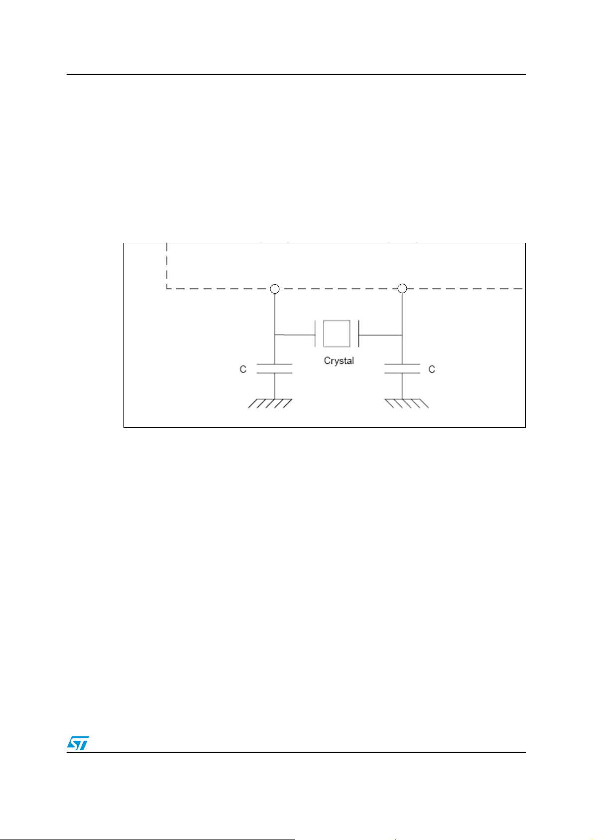
If an external crystal is used, SELCLK33 pin must be connected to GND and the suggested
circuit shown below should be used.
Figure 4. Circuit for crystal drive
STA529
External
components
Doc ID 13095 Rev 3 17/57
Page 18

Digital processing STA529
5 Digital processing
The STA529 processor block is a digital block providing two channels of audio processing
and channel-mapping capability.
5.1 Signal processing flow
I2S or stereo ADC data can be selected. The I2S frequency range is 8 kHz to 192 kHz. The
ADC sampling frequency can be selected between 8 kHz and 48 kHz.
5.2 I2C interface disable
When pin I2CDIS = 1, the SDA, SCL, LRCLKO and BICLKO pins can be pulled high or low
to change certain parameters of operation.
● SDA = 0: FFX input comes from ADC
SDA = 1: FFX input comes from digital audio interface
● SCL = 0: binary output mode (binary soft start/stop enabled)
SCL = 1: phase shift output mode
● LRCLKO = 0: no volume change
LRCLKO = 1: channel volume up on both channel
● BICLKO = 0: no volume change
BICLKO = 1: channel volume down on both xchannel.
At power up, the channel volume is set to -60 dB. When holding pin LRCLKO = 1 and pin
BICLKO = 1 simultaneously, the channel volume is set to 0 dB. A high pulse on pin LRCLKO
causes a channel volume change of +0.5 dB and a high pulse on pin BICLKO causes a
channel volume change of -0.5 dB.
18/57 Doc ID 13095 Rev 3
Page 19
STA529 Digital processing
5.3 Volume control and gain
The volume control structure of the STA529 consists of individual volume registers for each
channel and a master volume register that provides an offset to each channel’s volume
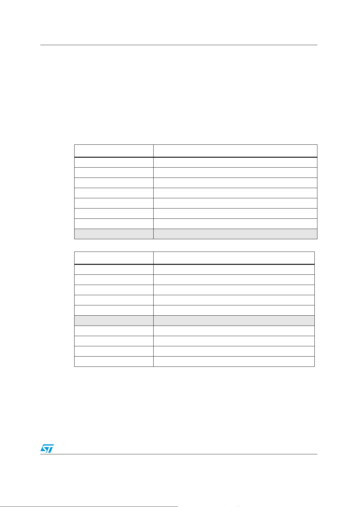
setting. The individual channel volumes are adjustable in 0.5-dB steps from +36 dB
to -91.5 dB. As an example, if register LVOL = 0x00 or +36 dB and register MVOL = 0x18
or -12 dB, then the total gain for the left channel is +24 dB.
When the mute bit is set to 1, all channels are muted. The volume control provides a soft
mute with the volume ramping down to mute in 4096 samples from the maximum volume
setting at the internal processing rate (around 48 kHz).
Table 13. Master volume offset as a function of register MVOL
MVOL[7:0] Volume offset from channel value
0x00 0 dB
0x01 -0.5 dB
0x02 -1dB
……
0x78 -60 dB
……
0xFE -105 dB
0xFF Hard master mute
Table 14. Channel volume as a function of registers LVOL and RVOL
LVOL/RVOL[7:0] Volume
0x00 +36 dB
0x01 +35.5 dB
0x02 +35 dB
……
0x47 +0.5 dB
0x48 0dB
0x49 -0.5 dB
……
……
0xFF -91.5 dB
Doc ID 13095 Rev 3 19/57
Page 20
PLL STA529
6 PLL
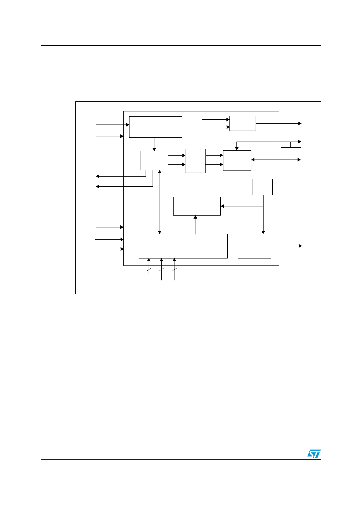
Figure 5 shows the main components of the PLL.
Figure 5. PLL block diagram
CLKIN
IDF
INFOUT
REFOUT
STRB
STRB_BYPASS
FRAC_CTRL
DITHER_DISABLE
Input frequency
divider
Buffer
FRAC_INPUT
INFIN
FBCLK
Fractional controller
Phase
frequency
divider
(PFD)
Loop frequency divider
NDIV
INFIN
FBCLK
Lock detect
Charge
pump and
loop filter
VCO
Output
frequency
divider
f
VCO
LOCKP
FILT
LF
VCONT
PHI
6.1 Functional description
Phase/frequency detector
The phase/frequency detector (PFD) compares the phase difference between the
corresponding rising edges of INFIN and FBCLK, (clock output from the loop frequency
divider) by generating voltage pulses with widths proportional to the input phase error.
Charge pump and loop filter
This block converts the voltage pulses from the phase/frequency detector to current pulses
which charge the loop filter and generate the control voltage for the voltage-controlled
oscillator. The loop filter is placed external to the PLL on pin FILT.
Voltage controlled oscillator
The voltage controlled oscillator (VCO) is the oscillator inside the PLL. It produces a
frequency (f
20/57 Doc ID 13095 Rev 3
) proportional to the input control voltage.
VCO
Page 21
STA529 PLL
Input frequency divider
This frequency divider divides the PLL input clock CLKIN by a factor called the input division
factor (IDF) to generate the PFD input frequency INFIN.
Loop frequency divider
This frequency divider is present within the PLL for dividing f
by a factor called the loop
VCO
division factor (LDF). The output of this block is clock FBCLK.
Output frequency divider
The output frequency divider divides f
output clock PHI and the clock to the core. In the STA529, ODF = 2 and cannot be
reconfigured.
by the output division factor (ODF) to produce the
VCO
Lock-detect circuit
The output of this block (signal LOCKP) is asserted high when the PLL enters the state of
Coarse Lock in which the output frequency is within ±10%, approximately, of the desired
frequency. LOCKP is refreshed every 32 cycles of clock INFIN. The generated value is
based on the result of comparing the number of FBCLK cycles in a window of 14 INFIN
cycles. The different cases generated after comparison are as follows.
● If LOCKP is already at 0, then in the next refresh cycle LOCKP goes to 1 if the number
of FBCLK cycles in the 14-cycle INFIN window is 13, 14, or 15. Otherwise LOCKP
stays at 0.
● If LOCKP is already at 1, then in the next refresh cycle LOCKP goes to 0 if the number
of FBCLK cycles in the 25-cycle INFIN window is less than 11 or higher than 17,
otherwise LOCKP stays at 1.
● If LOCKP is already at 1 and CLKIN is lost (no longer present on the input pin), LOCKP
stays at 1. In this case, the PLL is unlocked.
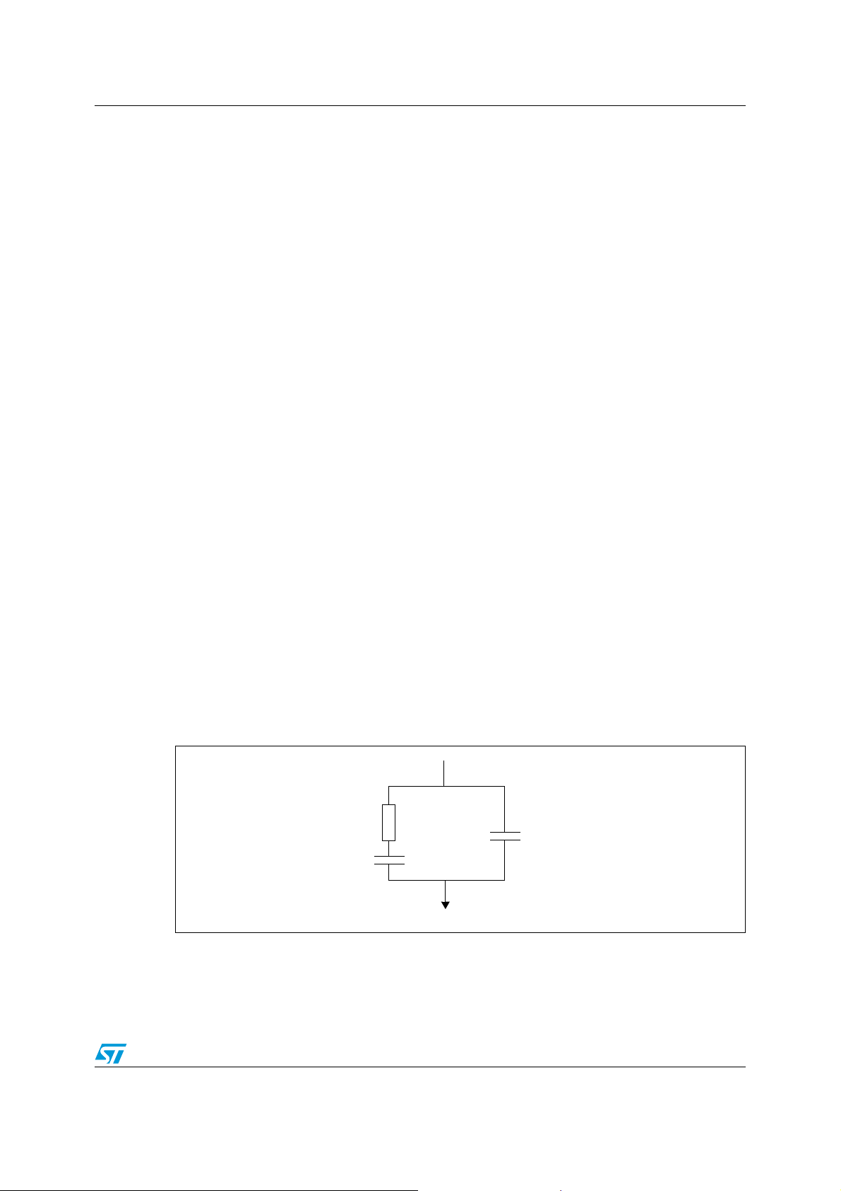
PLL filter
Figure 6 below shows the PLL filter circuit. Recommended values are R1 = 12.5 kΩ,
C1 = 250 pF and C2 = 82 pF.
Figure 6. PLL filter circuit
Vc
R1
C2
C1
Ground
Table 12 on page 16 gives a typical lock time value for the PLL.
Doc ID 13095 Rev 3 21/57
Page 22

PLL STA529
6.2 Configuration examples
The STA529 PLL can be configured in two ways:
● default startup configuration
● direct PLL programming
The default startup configuration reads the device defaults. With this configuration, it is not
necessary to program the PLL dividers directly as preset values are used. In this mode, the
oversampling ratio between pins XTI (or MCLK33) and LRCLKI is fixed to 256.
The direct PLL programming bypasses the automatic presets allowing direct programming
of the PLL dividers.
The output PLL frequency can be determined by the following equations.
Output division factor:
ODF = 2.
Relation between input and output clock frequency:
f
= f
INFIN
If register bit PLLCFG0.FRAC_CTRL = 1
f
= f
VCO
f
= f
PHI
When register bit PLLCFG0.DITHER_DISABLE[1] = 1, the 1/2
multiplication. This is recommended in order to keep register bit
PLLCFG0.DITHER_DISABLE[1] = 0, otherwise there can be spurious signals in the output
clock spectrum.
/ IDF.
XTI
* (LDF + FRACT / 216 + 1 / 217)
INFIN
/ ODF.
VCO
17
factor is not in the
If register bit PLLCFG0.FRAC_CTRL = 0, then:
f
VCO
f
PHI
= f
= f
INFIN
VCO
* LDF
/ ODF.
In the above equations:
FRACT = decimal equivalent of register bit PLLCFG1.FRAC_INPUT[15:0]
IDF = input division factor
LDF = loop division factor
ODF = output division factor = 2
f
= INFIN frequency
INFIN
f
= XTI frequency
XTI
f
= VCO frequency
VCO
f
= frequency of the PLL output clock.
PHI
When selecting the values for IDF, LDF and FRACT, ensure that the following limits are
maintained:
2.048 MHz < f
2.048 MHz < f
65.536 MHz < f
< 49.152 MHz
XTI
< 16.384 MHz
INFIN
< 98.304 MHz
VCO
There are also some additional constraints on IDF and LDF. IDF should be greater than 0,
LDF should be greater than 5 if FRAC_CTRL = 0 and greater than 8 if FRAC_CTRL = 1.
22/57 Doc ID 13095 Rev 3
Page 23
STA529 PLL
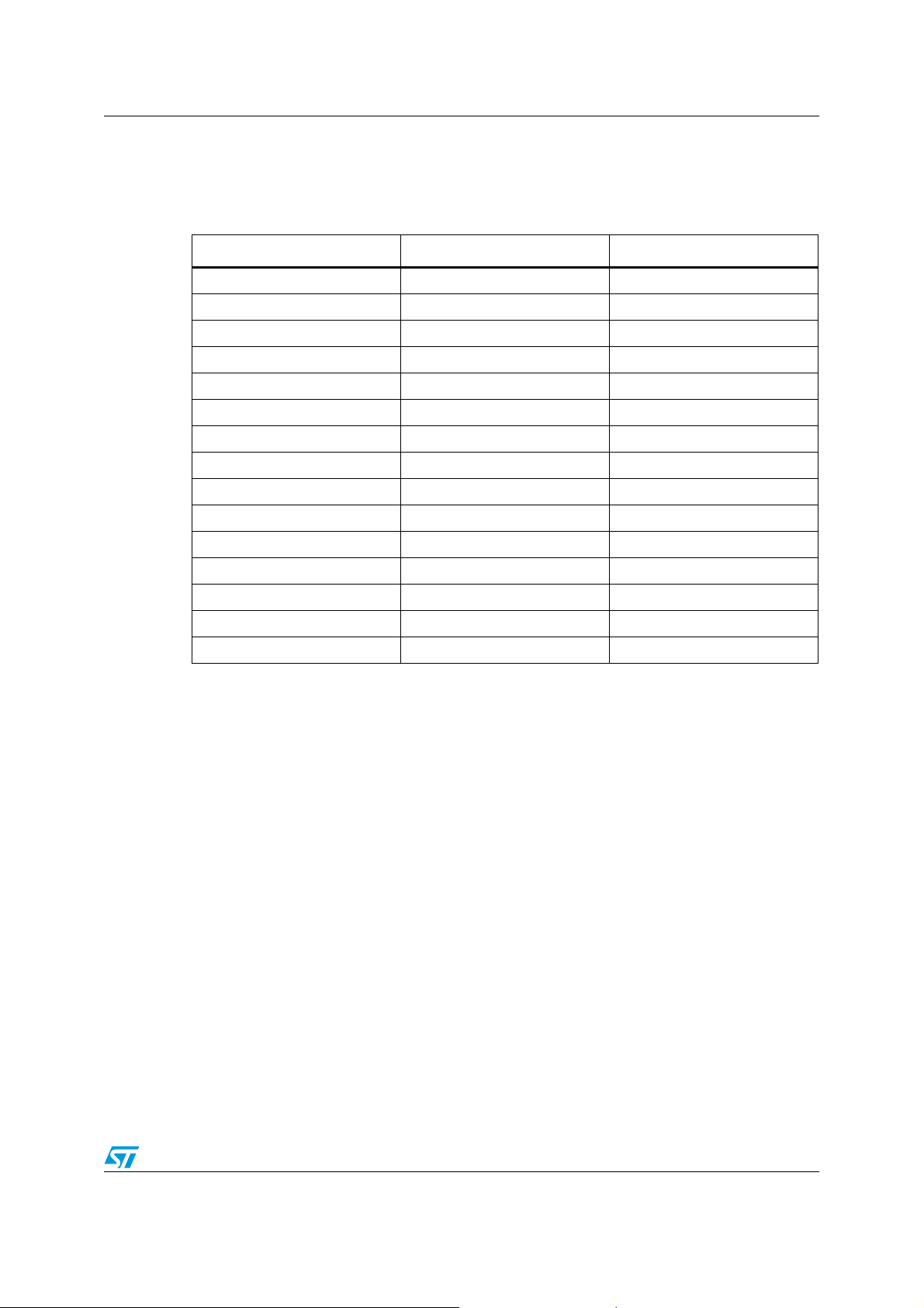
When automatic settings are not used, the PLL must be configured to generate an internal
frequency, f
, of N * fs, where fs is the frequency of pin LRCLKI. Values for N are given in
PHI
Ta bl e 1 5 .
Table 15. Oversampling table
fs (kHz) N f
8 4096 32.768
11.025 4096 45.1584
12 4096 49.152
16 2048 32.768
22.05 2048 45.1584
24 2048 49.152
32 1024 32.768
44.1 1024 45.1584
48 1024 49.152
64 512 32.768
88.2 512 45.1584
96 512 49.152
128 256 32.768
176.4 256 45.1584
192 256 49.152
Example 1
PHI
(MHz)
f
= 13 MHz and fs = 44.1 kHz
XTI
IDF should be equal to 3 otherwise LDF becomes less than 8 (FRAC_CTRL must be 1):
LDF = floor(45.1584 / (13 / IDF)) = 10
FRACT = round([(45.1584 / (13 / IDF)) - floor(45.1584 / (13 / IDF))] * 2
16
) = 27602.
where:
floor means rounded down and
round means rounded to nearest integer.
Using the above configuration, the system clock is 45.15841675 MHz, the approximate
static error is 16 Hz (that is, 0.5 ppm).
Example 2
f
= 19.2 MHz and fs = 48 kHz
XTI
IDF should be equal to 4 otherwise LDF become less than 8 (FRAC_CTRL must be 1):
LDF = floor(49.152 / (19.2 / IDF)) = 10
FRACT = round([(49.152 / (19.2 / IDF)) - floor(49.152 / (19.2 / IDF))] * 2
Using the above configuration, the system clock is 49.151953125 MHz, the approximate
static error is 47 Hz (that is, 1 ppm).
Doc ID 13095 Rev 3 23/57
16
) = 15728.
Page 24

PLL STA529
6.3 Set fractional PLL
The following procedure is mandatory to configure the fractional PLL:
1. Set bit D7 reg 0x18 ( PLL_BYP_UNL) to "1"
2. Write reg 0x17 (PLLCFG3)
3. Write reg 0x14 (PLLCFG0)
4. Write reg 0x15 (PLLCFG1)
5. Write reg 0x16 (PLLCFG2)
6. Set bit D7 reg 0x18 ( PLL_BYP_UNL) to "0"
24/57 Doc ID 13095 Rev 3
Page 25
STA529 ADC
7 ADC
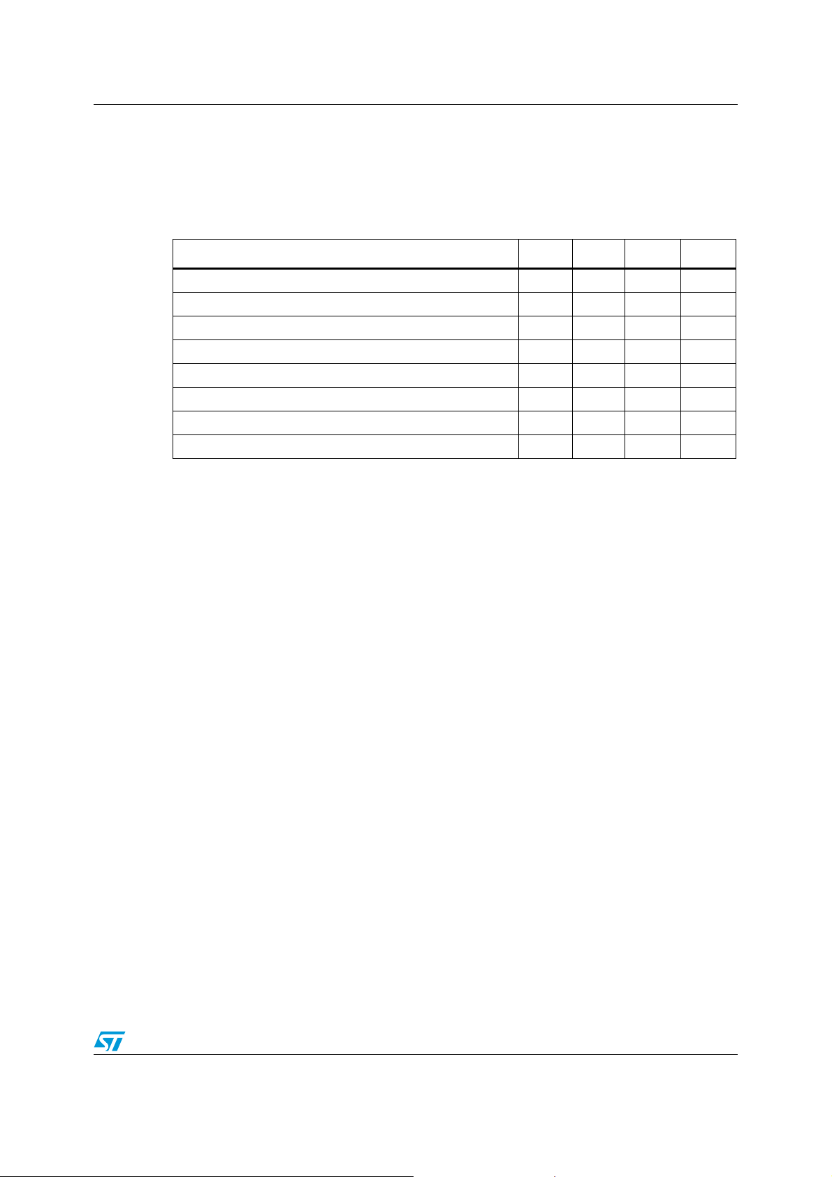
7.1 ADC performance values
Table 16. Programmable gain performance
Parameter Min Typ Max Unit
Dynamic range 1 kHz, A-weighted (3.3 V supply) 92 dB
Dynamic range 1 kHz, A-weighted (1.8 V supply) 84 dB
SNDR 1 kHz, A-weighted (3.3 V supply) 92 dB
SNDR 1 kHz, A-weighted (1.8 V supply) 84 dB
THD 1 kHz (-1 dB input) (3.3 V supply) -85 dB
THD 1 kHz (-1 dB input) (1.8 V supply) -75 dB
Cross talk (3.3 V supply) -80 dB
Cross talk (1.8 V supply) -60 dB
7.2 Functional description
The STA529 analog input is provided through a low-power, low-voltage, 16-bit stereo audio
analog-to-digital converter front end designed for audio applications. It includes a
programmable gain amplifier, anti-aliasing filter, low-noise microphone biasing circuit,
third-order MASH2-1 delta-sigma modulator, digital decimating filter and a first-order
DC-removal filter.
The ADC works in the microphone input (mic-in) mode and in the line-input mode. If the line
input mode is selected, the ADC is configured in stereo and all conversion channels are
active.
If the microphone input mode is selected, the ADC is configured in mono. The mono
channel is routed through the left conversion path, and the right conversion path is kept in
power-down mode to minimize power consumption. A programmable gain amplifier (PGA) is
available in mic-in mode, making it possible to amplify the signal from 0 to +42 dB in steps of
6dB.
Doc ID 13095 Rev 3 25/57
Page 26
ADC STA529
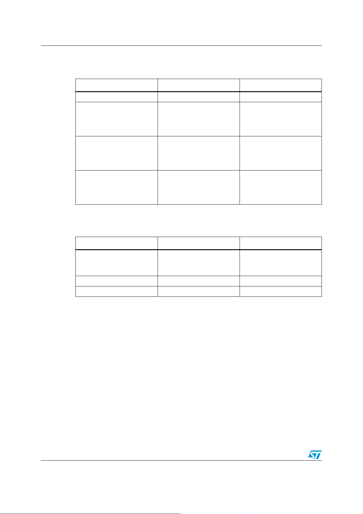
7.2.1 Digital filter characteristics
Table 17. Digital filter characteristics
Parameter Typical Unit
Pass band 0.4535 * fs kHz
Pass-band ripple:
Fs mode
Fs_by_2 mode
Fs_by_4 mode
Stop-band attenuation:
Fs mode
Fs_by_2 mode
Fs_by_4 mode
Group delay:
Fs mode
Fs_by_2 mode
Fs_by_4 mode
0.08 at 44.1 kHz
0.08 at 22.05 kHz
0.08 at 11.025 kHz
45 at 44.1 kHz
45 at 22.05 kHz
45 at 11.025 kHz
0.4 at 32 kHz
0.7 at 16 kHz
1.4 at 8 kHz
dB
dB
dB
dB
dB
dB
ms
ms
ms
7.2.2 High-pass filter characteristics
Table 18. High-pass filter characteristics
Parameter Typical Unit
Frequency response:
-3 dB
-0.08 dB
7
50
Phase deviation at 20 Hz 19.35 degree
Passband ripple 0.08 dB
7.2.3 Programmable gain amplifier (PGA)
The PGA is available in mic-in mode only. The input signal can be amplified from 0 to 42 dB
in 6-dB steps via bits PGA of register ADCCFG on page 49.
Hz
Hz
26/57 Doc ID 13095 Rev 3
Page 27
STA529 ADC
7.3 Applications scheme
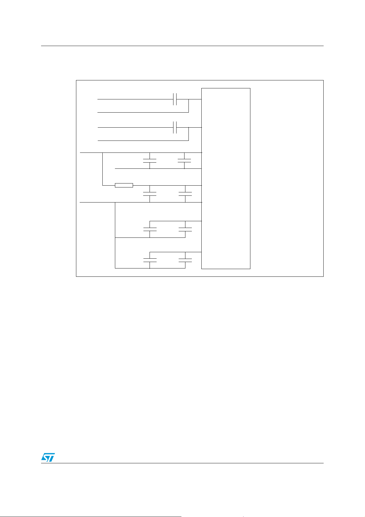
Figure 7. Diagram of input coupling and supply decoupling
C9
AC coupled
DC coupled
AC coupled
DC coupled
3V, 3A supply
VSSA
VSSA
R1
C5
C6
C7
C8
INL
C0
INR
AVD D
C1
AGND
VHI
C2
VLO
VCM
C3
VBIAS
C4
C1, C2, C3, C4 = 10 nF
(These capacitors must be
placed very close to their
respective IC pins)
C5, C6, C7 = 33 µF
(Low ESR and ESL
capacitors are
recommended)
C8 = 10 µF
C9, C0 = 1 µF
R1 = 500 Ω
VSSA plane must be
different from other
ground plane
3V, 3A must be a
low-noise supply and
separate from
other supplies
7.4 Configuration examples
The ADC sampling frequency can be selected from three values:
● normal (from 32 kHz to 48 kHz)
● low (from 16 kHz to 24 kHz)
● very-low (from 8 kHz to 12 kHz)
The setting is done through bits ADC_FS_RANGE of register MISC on page 50. For all
other settings register ADCCFG on page 49 is used.
Doc ID 13095 Rev 3 27/57
Page 28
Driver configuration STA529
8 Driver configuration
A driver configuration is available that allows PWM commands to be used on an external
power device. For this purpose, the output serial audio interface is disabled and the
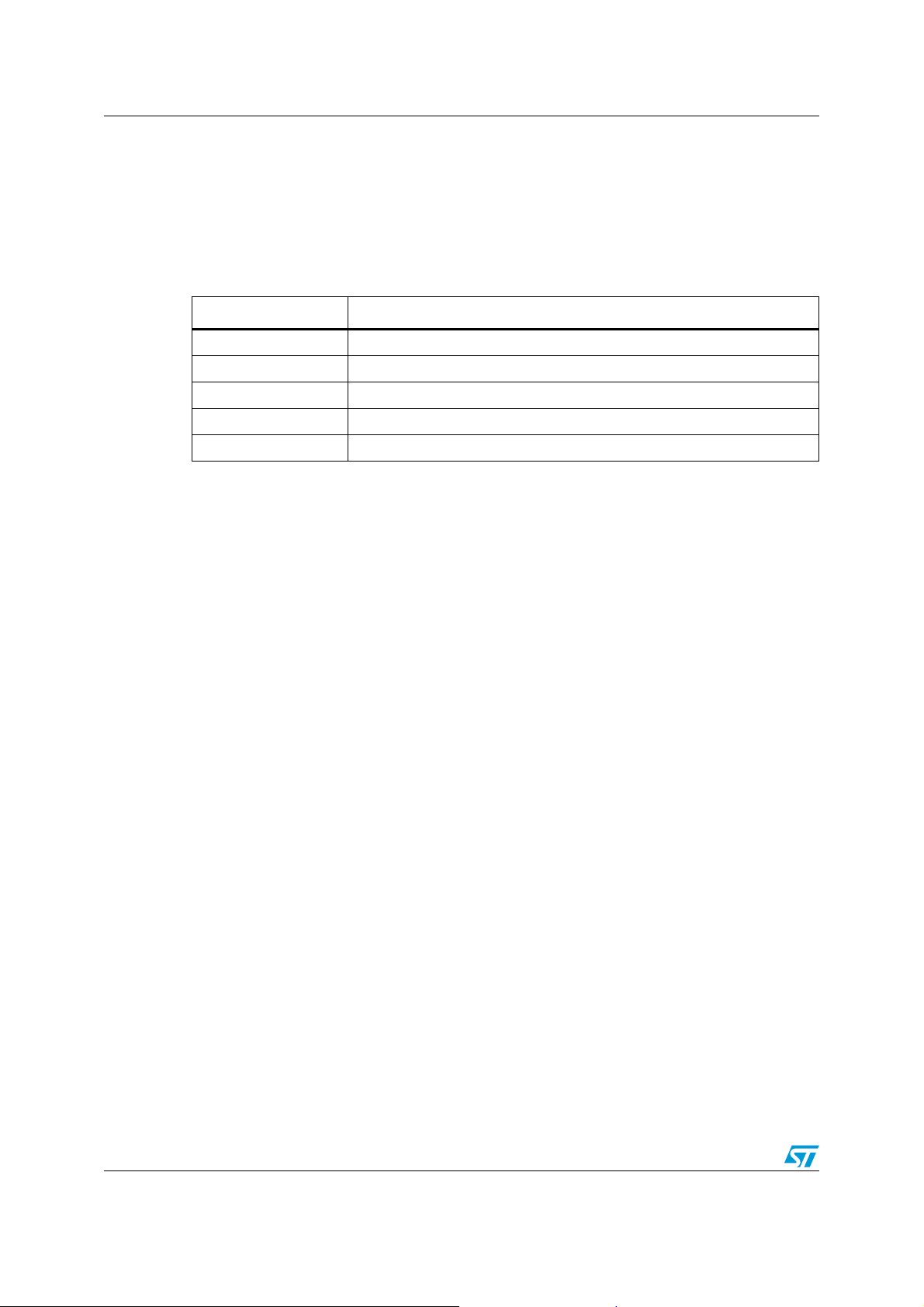
respective pins have an alternative name and a new function, as shown in Tab le 1 9 .
Table 19. Pin functions in driver-configuration mode
Pin Alternative pin name and function
BICLKO PWM1A (external bridge PWM command for output 1A)
LRCLKO PWM1B (external bridge PWM command for output 1B)
SDATAO PWM2A (external bridge PWM command for output 2A)
CLKOUT PWM2B (external bridge PWM command for output 2B)
POWERFAULT EADP (external audio power-down signal)
The driver configuration is selected with the two programmable registers, PWMINT1 = 0x93
and PWMINT2 = 0x81, on page 51.
8.1 I2S bypass
A configuration is available which allows the passing of the I2S input signal straight to the
2
I
S output signal.
This configuration is set using two programmable registers PWMINT1 = 0x93 and
PWMINT2 = 0x80.
28/57 Doc ID 13095 Rev 3
Page 29
STA529 Serial audio interface
9 Serial audio interface
The serial-to-parallel interface and the parallel-to-serial interface can have different
sampling rates.
The following terms are used in this section:
● BICLK active edge: Pins SDATAI, SDATAO, LRCLKI, LRCLKO always change
synchronously with BITCLK active edges. The active edge can be configured as a
rising or falling edge via register programming.
● BICLK strobe edge: Pins SDATAI, SDATAO, LRCLKI, LRCLKO should be stable near
BICLK strobe edges, the slave device is able to use strobe edges to latch serial data
internally.
9.1 Master mode
In this mode, pins BICLKI/BICLKO and pins LRCLKI/LRCLKO are configured as outputs.
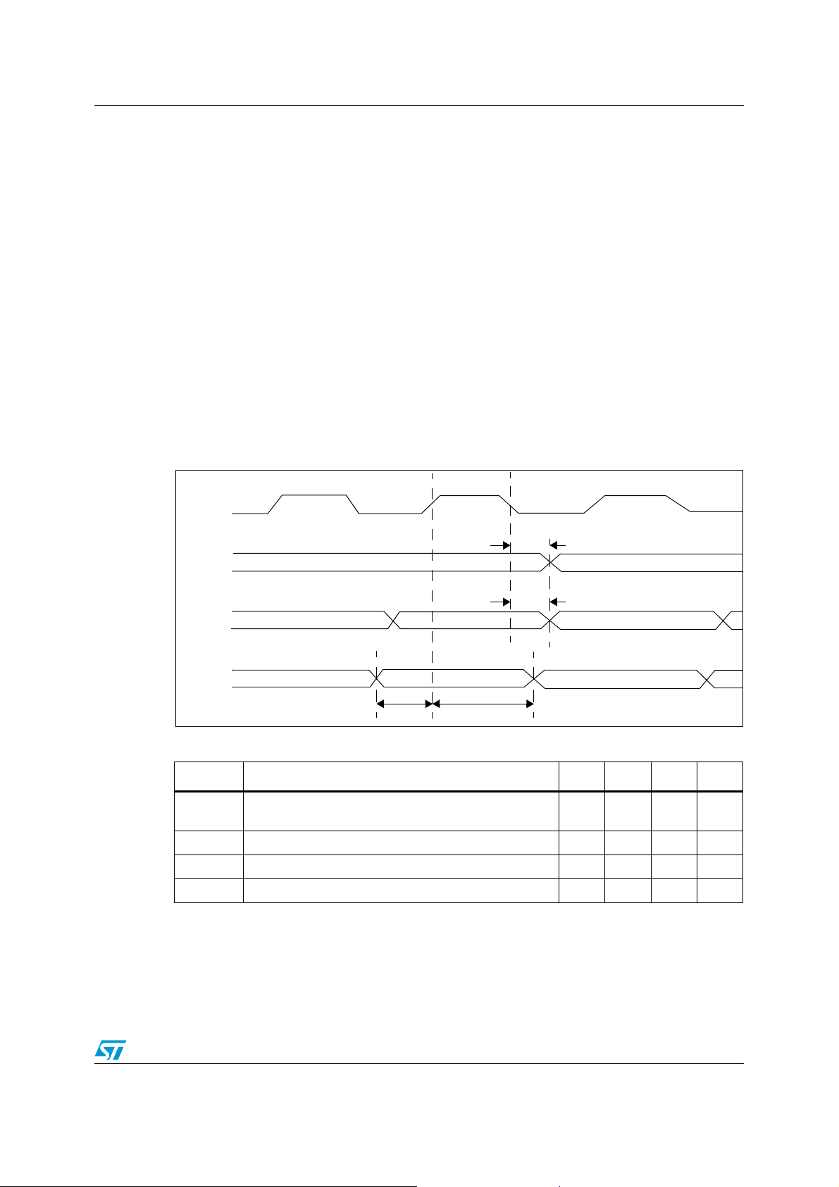
Figure 8. Master mode
BICLKI/
BICLKO
t
LRCLKI/
DL
LRCLKO
t
DDA
SDATAO
SDATAI
Table 20. Master mode
t
DST
t
DHT
Symbol Parameter Min Typ Max Unit
t
DL
t
DDA
t
DST
t
DHT
LRCLKI/LRCLKO propagation delay from BICLK active
edge
010ns
SDATAO propagation delay from BICLKI/O active edge 0 15 ns
SDATAI setup time to BICLKI/O strobing edge 10 ns
SDATAI hold time from BICLKI/O strobing edge 10 ns
Doc ID 13095 Rev 3 29/57
Page 30
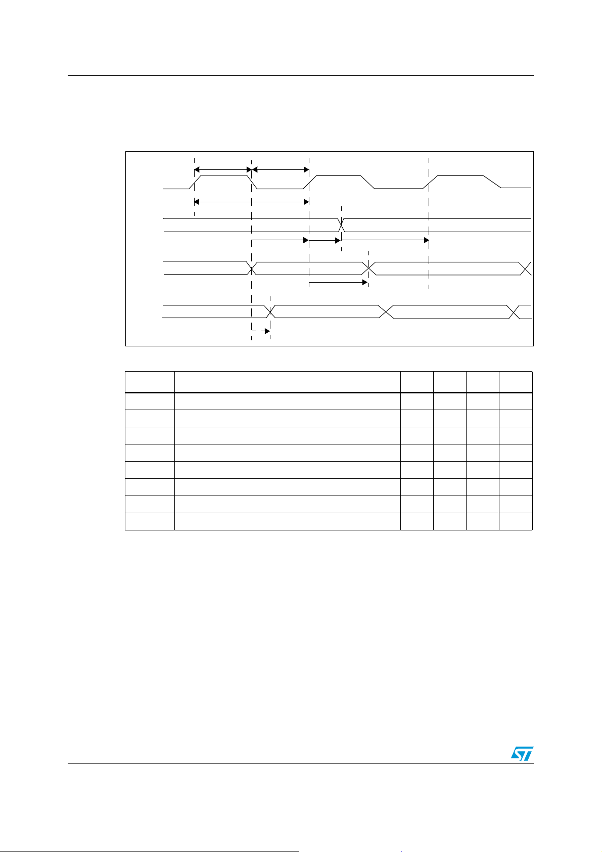
Serial audio interface STA529
9.2 Slave mode
In this mode, pins BICLKI/O and pins LRCLKI/O are configured as inputs.
Figure 9. Slave mode
t
BCH
t
BCL
BICLKI/
BICLKO
t
BCY
LRCLKI/
LRCLKO
t
DS
t
LRH
t
LRSU
SDATAI
t
DH
SDATAO
t
DD
Table 21. Slave mode
Symbol Parameter Min Typ Max Unit
t
BCY
t
BCH
t
BCL
t
LRSU
t
LRH
t
DS
t
DH
t
DD
BICLK cycle time 50 ns
BICLK pulse width high 20 ns
BICLK pulse width low 20 ns
LRCLKI/LRCLKO setup time to BICLK strobing edge 10 ns
LRCLKI/LRCLKO hold time to BICLK strobing edge 10 ns
SDATAO setup time to BICLK strobing edge 25 ns
SDATAO hold time to BICLK strobing edge 25 ns
SDATAI propagation delay from BICLK active edge 0 10 ns
30/57 Doc ID 13095 Rev 3
Page 31
STA529 Serial audio interface
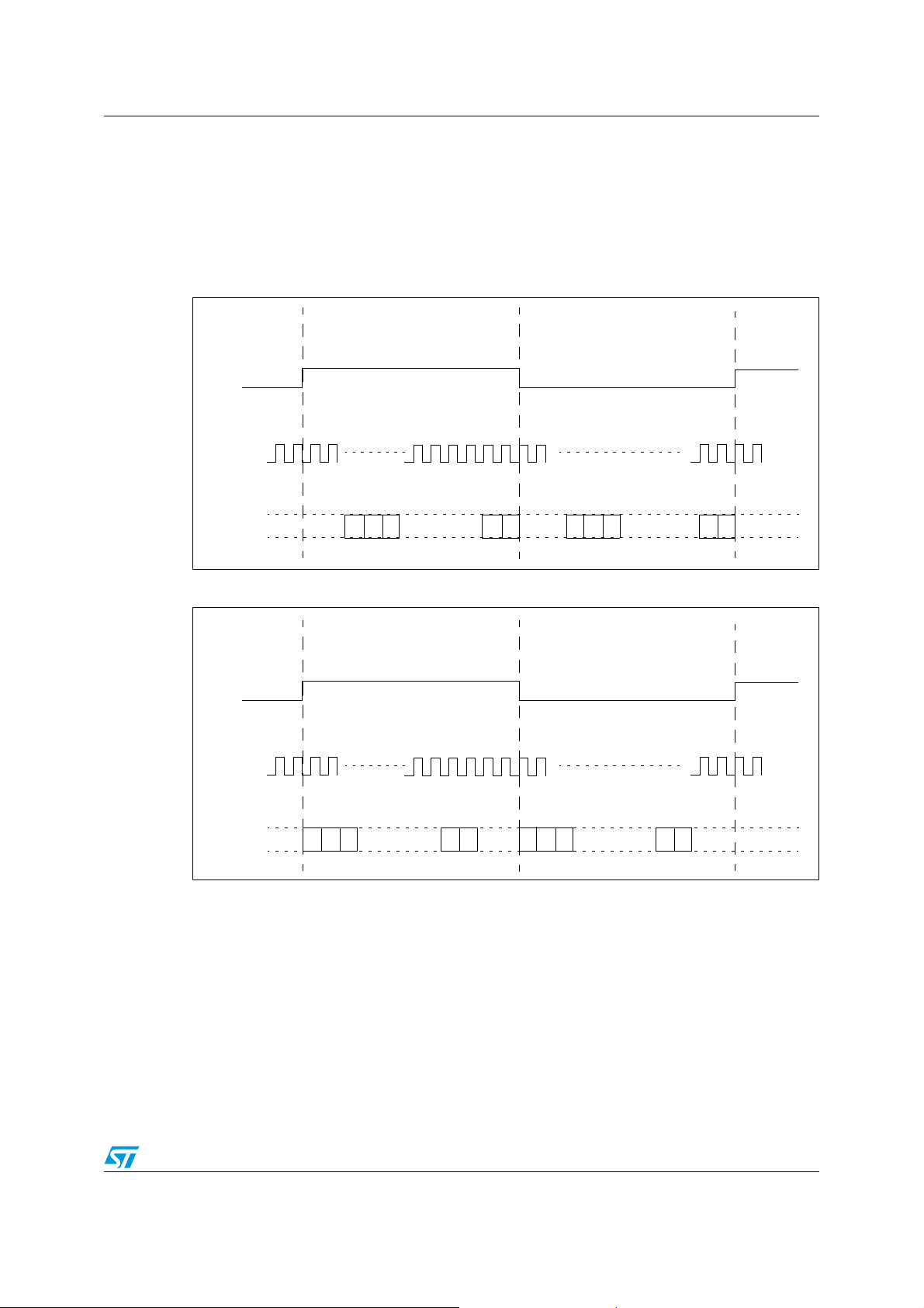
9.3 Serial formats
Different audio formats are supported in both master and slave modes. Clock and data
configurations can be customized to match most of the serial audio protocols available on
the market.
Data length can be customized to 8, 16, 24 or 32 bits.
Figure 10. Right justified
LRCLKI/
LRCLKO
BICLKI/
BICLKO
SDATAI/
SDATAO
123
Figure 11. Left justified
LRCLKI/
LRCLKO
BICLKI/
BICLKO
SDATAI/
SDATAO
123
n-1n
n
-1
n
123
123
n
n
-1
n
n
-1
Doc ID 13095 Rev 3 31/57
Page 32
Serial audio interface STA529
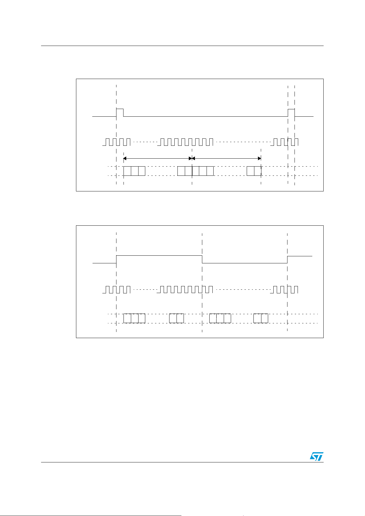
9.3.1 DSP
Figure 12. DSP
LRCLKI/
LRCLKO
BICLKI/
BICLKO
Left Right
9.3.2 I2S
Figure 13. I2S
SDATAI/
SDATAO
LRCLKI/
LRCLKO
BICLKI/
BICLKO
SDATAI/
SDATAO
123
123
n-1n
123
n
n
-1
123
n
n
-1
n
n
-1
32/57 Doc ID 13095 Rev 3
Page 33
STA529 Serial audio interface
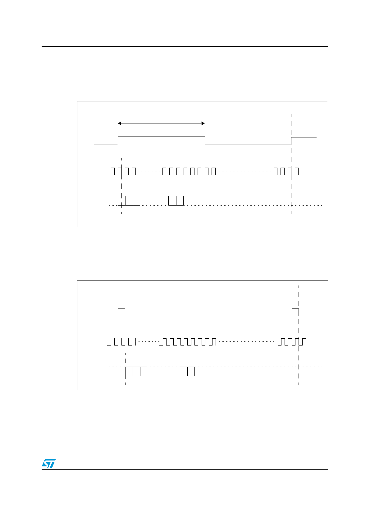
9.3.3 PCM/IF (non-delayed mode)
● MSB first
● 16-bit data
Figure 14. PCM/IF (non-delayed mode)
Any width
LRCLKI/
LRCLKO
BICLKI/
BICLKO
SDATAI/
SDATAO
123
9.3.4 PCM/IF (delayed mode)
● MSB first
● 16-bit data
Figure 15. PCM/IF (delayed mode)
LRCLKI/
LRCLKO
BICLKI/
BICLKO
SDATAI/
SDATAO
123
n
n
-1
n
n
-1
Doc ID 13095 Rev 3 33/57
Page 34

I2C interface STA529
10 I2C interface
10.1 Data transition and change
Data changes on the SDA line must only occur when the SCL clock is low. SDA transition
while the clock is high is used to identify a start or stop condition.
10.2 Start condition
A start condition is identified by a high to low transition of the data bus SDA signal while the
clock signal SCL is stable in the high state. A start condition must precede any command for
data transfer.
10.3 Stop condition
A stop condition is identified by low to high transition of the data bus SDA signal while the
clock signal SCL is stable in the high state. A stop condition terminates communication
between the STA529 and the master bus.
10.4 Data input
During data input, the STA529 samples the SDA signal on the rising edge of clock SCL. For
correct device operation the SDA signal must be stable during the rising edge of the clock
and the data can change only when the SCL line is low.
10.5 Device addressing
To start communication between the master and the STA529, the master must initiate with a
start condition. Following this, the master sends 8 bits (MSB first) on the SDA line
corresponding to the device select address and read or write mode.
The 7 most significant bits are the device address identifiers, corresponding to the I
definition. In the STA529, the I
The 8th bit (LSB) identifies the read or write operation (R/W). It is set to 1 in read mode and
0 in write mode.
After the start condition, the STA529 waits for its device address on SDA. When a match is
found, it acknowledges the identification on SDA during the 9th bit time. The byte following
the device identification byte is the internal space address.
2
C interface has the device address 0x34.
2
C bus
34/57 Doc ID 13095 Rev 3
Page 35

STA529 I2C interface
10.6 Write operation
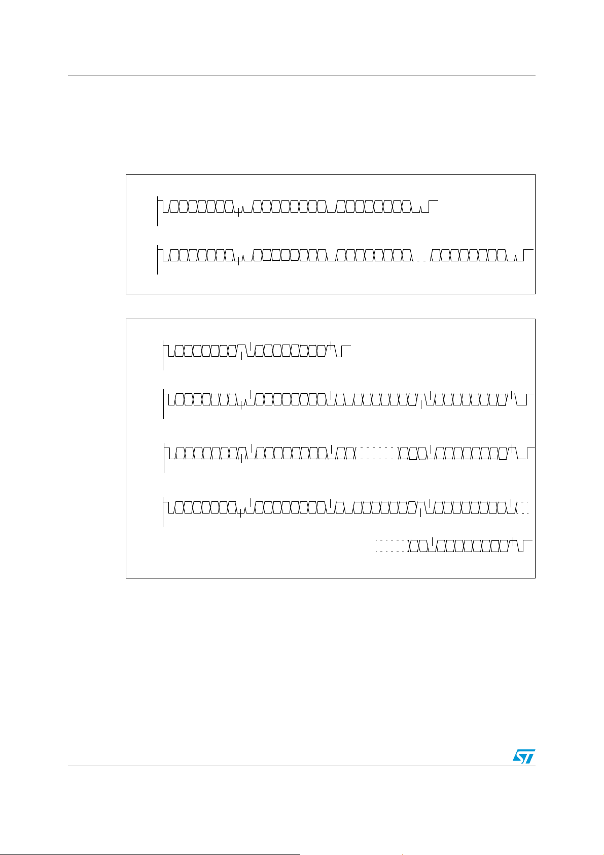
Following the start condition the master sends a device select code with the R/W bit set to 0.
The STA529 acknowledges this and then writes to the byte of the internal address. After
receiving the internal byte address, the STA529 responds with an acknowledgement.
10.6.1 Byte write
In the byte-write mode the master sends one data byte. This is acknowledged by the
STA529. The master then terminates the transfer by generating a stop condition.
10.6.2 Multi-byte write
The multi-byte write modes can start from any internal address. The master generates a
stop condition which terminates the transfer.
10.7 Read operation
10.7.1 Current address byte read
Following the start condition the master sends a device select code with bit R/W set to 1.
The STA529 acknowledges this and then responds by sending one byte of data. The master
then terminates the transfer by generating a stop condition.
10.7.2 Current address multi-byte read
The multi-byte read modes can start from any internal address. Sequential data bytes are
read from sequential addresses within the STA529. The master acknowledges each data
byte read and then generates a stop condition terminating the transfer.
10.7.3 Random address byte read
Following the start condition the master sends a device select code with bit R/W set to 0.
The STA529 acknowledges this and then the master writes the internal address byte. After
receiving the internal byte address, the STA529 again responds with an acknowledgement.
The master then initiates another start condition and sends the device select code with bit
R/W set to 1. The STA529 acknowledges this and then responds by sending one byte of
data. The master then terminates the transfer by generating a stop condition.
Doc ID 13095 Rev 3 35/57
Page 36
I2C interface STA529
10.7.4 Random address multi-byte read
The multi-byte read modes could start from any internal address. Sequential data bytes are
read from sequential addresses within the STA529. The master acknowledges each data
byte read and then generates a stop condition terminating the transfer.
Figure 16. I
Byte
Write
Start
Multibyte
Write
Start
Dev address
Figure 17. I
Current
address
read
Start
Random
address
read
Sequential
current
read
2
C write operations
ACK
Dev address
2
C read operations
Dev address
Dev address
Dev address
R/W
ACK
R/W
ACK
R/W
ACK
R/W
ACK
R/W=High
Sub address
Sub address
Data
Data
ACK
ACK
No ACK
Stop
ACK
ACK
ACK
Data in
ACK ACK
Data in
Dev address R/W
Data
Stop
ACK
ACK
Data in
Data
Stop
No ACK
StopStart Sub address Start Data
No ACK
StopStart
Sequential
random
read
ACK
Start Sub address Start Data
Dev address
R/W
ACK
36/57 Doc ID 13095 Rev 3
Dev address R/W
Data
ACK
ACK
ACK
No ACK
StopData
Page 37
STA529 Registers
11 Registers
This section describes the set-up register used in the device.
11.1 Summary
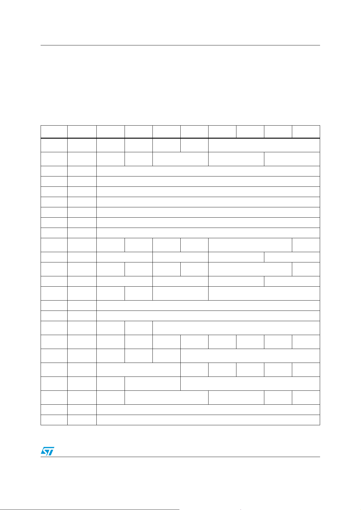
Table 22. Register summary
Address Name Bit 7 Bit 6 Bit 5 Bit 4 Bit 3 Bit 2 Bit 1 Bit 0
0x00 FFXCFG0
0x01 FFXCFG1
0x02 MVOL
0x03 LVOL
0x04 RVOL
0x05 TTF0
0x06 TTF1
0x07 TTP0
0x08 TTP1
0x0A S2PCFG0
0x0B S2PCFG1
0x0C P2SCFG0
0x0D P2SCFG1
0x14 PLLCFG0
0x15 PLLCFG1
0x16 PLLCFG2
0x17 PLLCFG3
0x18 PLLPFE
0x19 PLLST
0x1E ADCCFG
0x1F CKOCFG
0x20 MISC
0x21 PADST0
0x22 PADST1
MUTE POW_STBY
L1_R2
BICLK_
STRB
PDATA_LENGTH[1:0] BICLK_OS[1:0] MAP_L[1:0] MAP_R[1:0]
BICLK_
STRB
PDATA_LENGTH[1:0] BICLK_OS[1:0] MAP_L[1:0] MAP_R[1:0]
PLL_DIREC
T_PROG
STRB
PLL_
BYP_ UNL
PLL_
UNLOCK
CLKOUT_
DIS
OSC_DIS P2P_FS_RANGE[2:0] ADC_FS_RANGE[1:0]
MUTE_ON_
INVALID
LRCLK_
LEFT
LRCLK_
LEFT
FRAC_
CTRL
STRB_
BYPASS
BICLK2PLL PLL_PWDN PFE1A PFE1B PFE2A PFE2B
PLL_PWD_
STATE
PGA[2:0] INSEL STBY
CLKOUT_SEL[1:0] Reserved
SOFT_
VOL_ON
PWM_MODE[1:0] PWM_SHIFT[1:0] Reserved
SHARE_
BILR
SDATAO_
ACT
DITHER_DISABLE[1:0] IDF[3:0]
PLL_BYP_
STATE
BIN_SOFT
START
SET_VOL_MASTER[7:0]
SET_VOL_LEFT[7:0]
SET_VOL_RIGHT[7:0]
TIM_TS_FAULT[15:8]
TIM_TS_FAULT[7:0]
TIM_TS_POWUP[15:8]
TIM_TS_POWUP[7:0]
MSB_FIRST DATA_FORMAT[2:0]
MSB_FIRST DATA_FORMAT[2:0]
FRAC_INPUT[15:8]
FRAC_INPUT[7:0]
Reserved
Reserved
NDIV[5:0]
Reserved
BYPASS_
TIM_SOFT_VOL[3:0]
CALIB
MASTER_
MODE
MASTER_
MODE
RESET_
FAU LT
CLKENBL Reserved
P2P_IN_
ADC
CORE_
CLKENBL
Doc ID 13095 Rev 3 37/57
Page 38
Registers STA529
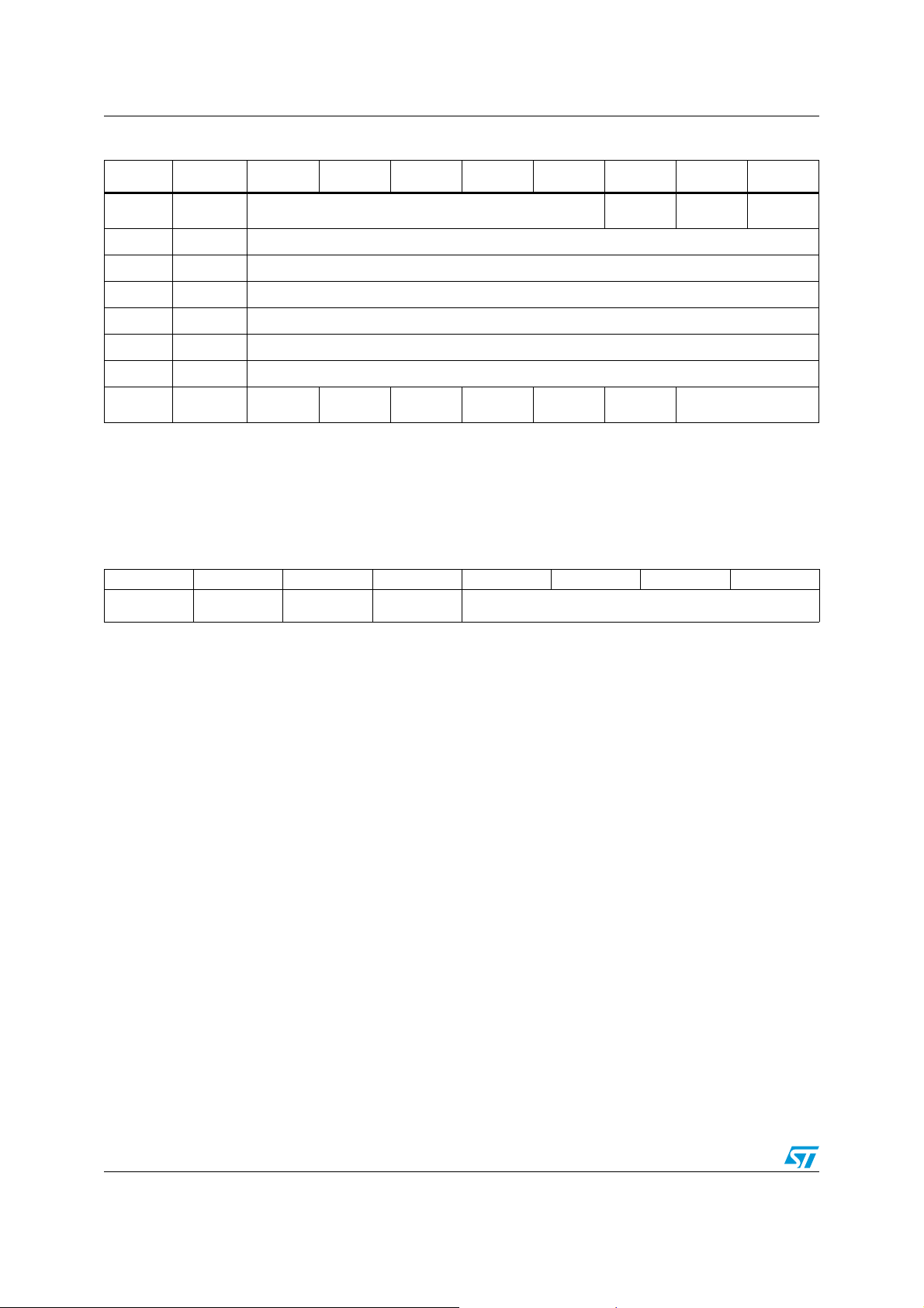
Table 22. Register summary (continued)
Address Name Bit 7 Bit 6 Bit 5 Bit 4 Bit 3 Bit 2 Bit 1 Bit 0
0x23 FFXST
0x28 BISTRUN
0x29 BISTST0
0x2A BISTST1
0x2B BISTST2
0x2D PWMINT1
0x2E PWMINT2
0x32 POWST
POWER
DOWN
POW_
TRISTATE
Reserved
POW_
FAU LT1 A
Reserved
Reserved
Reserved
Reserved
PWM_INT[15:8]
PWM_INT[7:0]
POW_
FAU LT1 B
POW_
FAU LT2A
INVALID_
INP_FBK
POW_
FAU LT2 B
MUTE_
INT_FBK
Reserved
Reserved
All other registers not mentioned here are reserved and must not be used.
11.2 General registers
FFXCFG0 FFX configuration
Bit 7 Bit 6 Bit 5 Bit 4 Bit 3 Bit 2 Bit 1 Bit 0
MUTE POW_STBY SOFT_VOL_ON
Address: 0x00
BIN_
SOFTSTART
TIM_SOFT_VOL[3:0]
Type: R/W
Buffer: No
Reset: 0x75
Description:
7MUTE:
0: standard operation (default)
1: FFX output is zero (muted condition)
6POW_STBY:
0: FFX bridge is in power-up mode
1: FFX bridge is in standby mode (default)
5 SOFT_VOL_ON:
0: smooth transition not active
1: smooth transition when changing volume control (default)
4 BIN_SOFTSTART:
Reserved (1: default)
3:0 TIM_SOFT_VOL: volume control time step for any 0.5 dB volume change
Time is (2
Default value: 0101. This value means 666.66 µs
TIM_SOFT_VOL
) * 20.83 µs
38/57 Doc ID 13095 Rev 3
Page 39
STA529 Registers
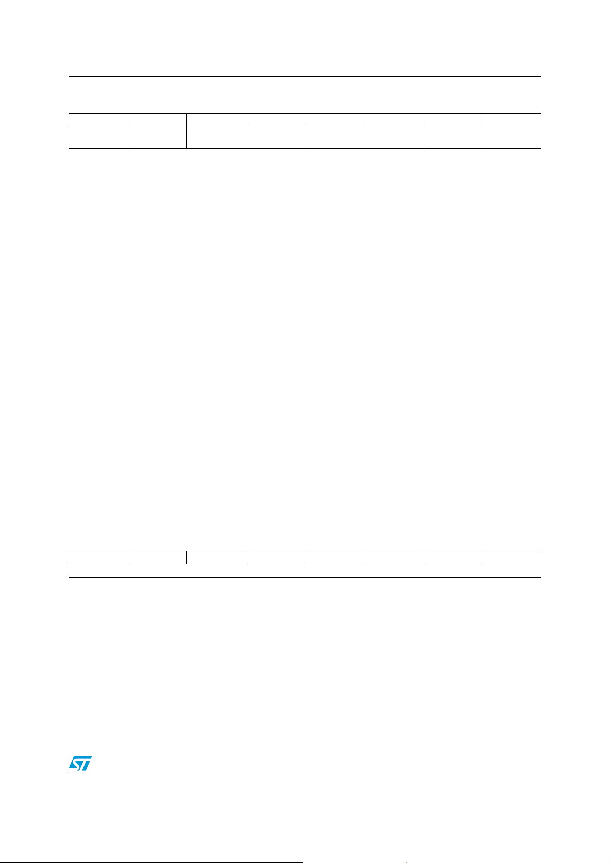
FFXCFG1 Configuration
Bit 7 Bit 6 Bit 5 Bit 4 Bit 3 Bit 2 Bit 1 Bit 0
L1_R2
Address: 0x01
Type: R/W
Buffer: No
Reset: 0xF8
Description:
MUTE_ON_
INVALID
PWM_MODE[1:0] PWM_SHIFT[1:0] RES RES
7 L1_R2: channel mapping:
0: right channel is mapped to output channel 1 and left channel is mapped to output
channel 2
1: left channel is mapped to output channel 1 and right channel is mapped to output
channel 2 (default)
6 MUTE_ON_ INVALID: mutes PWM outputs if invalid digital data is received:
0: outputs are not muted
1: outputs are muted (default)
5:4 PWM_MODE[1:0]:
00: binary (output B is opposite of output A)
01: binary headphones (output B is 50% duty cycle)
10: reserved, do not use
11: phase shift (default)
3:2 PWM_SHIFT[1:0]:
10: default
PWM period-shift between channels 1 and 2
Value is N * 90
Default is 180
o
o
1:0 Reserved (00: default)
MVOL Master volume control
Bit 7 Bit 6 Bit 5 Bit 4 Bit 3 Bit 2 Bit 1 Bit 0
SET_VOL_MASTER[7:0]
Address: 0x02
Type: R/W
Buffer: No
Reset: 0x00
Description:
7:0 SET_VOL_MASTER[7:0]: master volume control:
From 0 dB to -127.5 dB in 0.5-dB steps
Default value (0x00) corresponds to 0 dB
Doc ID 13095 Rev 3 39/57
Page 40
Registers STA529
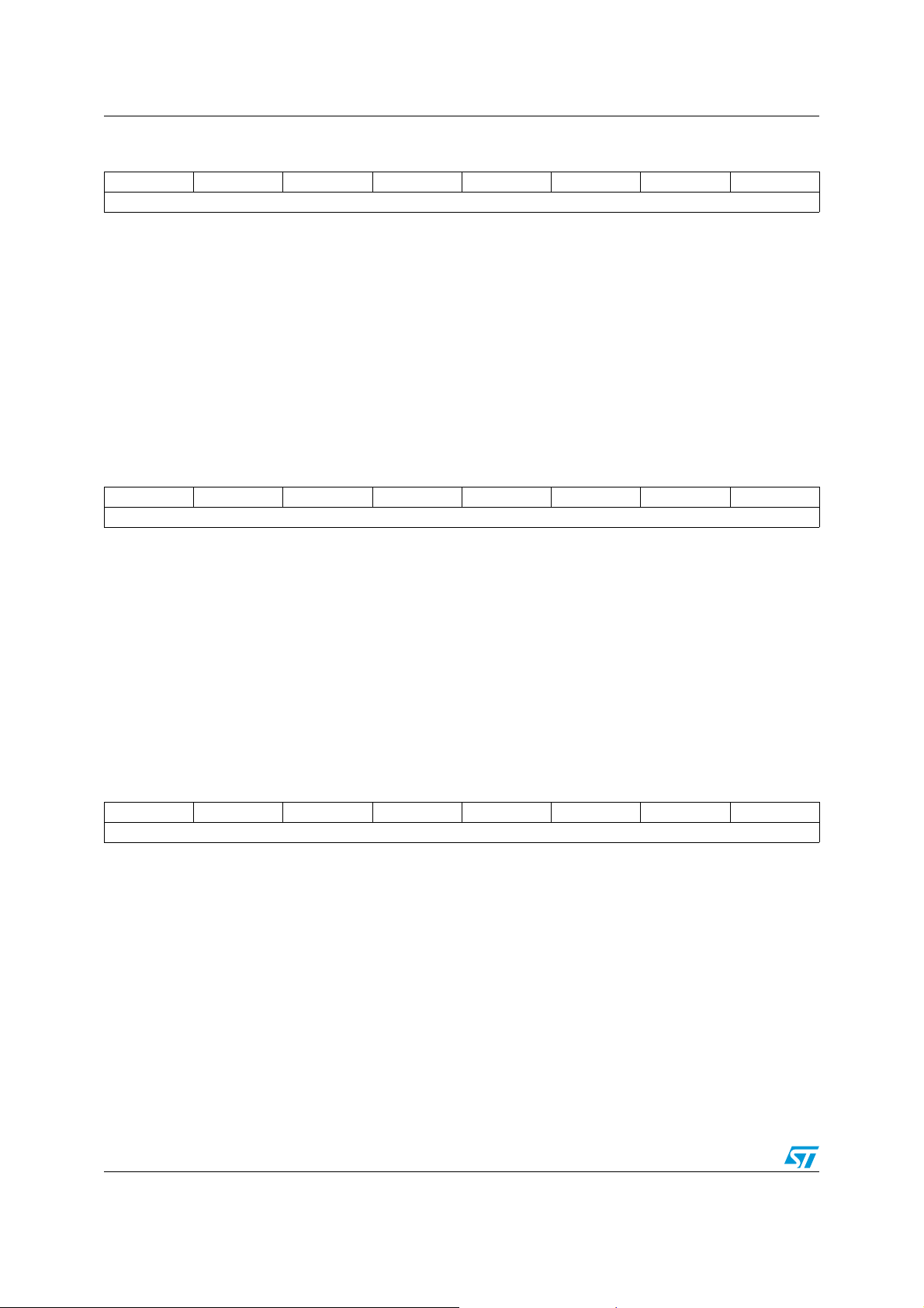
LVOL Left channel volume control
Bit 7 Bit 6 Bit 5 Bit 4 Bit 3 Bit 2 Bit 1 Bit 0
SET_VOL_LEFT[7:0]
Address: 0x03
Type: R/W
Buffer: No
Reset: 0x48
Description:
7:0 SET_VOL_LEFT[7:0]: left channel volume control:
Left channel volume control (from +36 dB to -91.5 dB in 0.5-dB steps)
Default value (0x48) corresponds to 0 dB
RVOL Right channel volume control
Bit 7 Bit 6 Bit 5 Bit 4 Bit 3 Bit 2 Bit 1 Bit 0
SET_VOL_RIGHT[7:0]
Address: 0x04
Type: R/W
Buffer: No
Reset: 0x48
Description:
7:0 SET_VOL_RIGHT[7:0]: right channel volume control:
Right channel volume control (from +36 dB to -91.5 dB in 0.5-dB steps)
Default value (0x00) corresponds to 0 dB
TTF0 Tristate time after fault (MSBs)
Bit 7 Bit 6 Bit 5 Bit 4 Bit 3 Bit 2 Bit 1 Bit 0
TIM_TS_FAULT[15:8]
Address: 0x05
Type: R/W
Buffer: No
Reset: 0x00
Description:
7:0 MSBs of TIM_TS_FAULT[15:0]:
See register TTF1.
40/57 Doc ID 13095 Rev 3
Page 41
STA529 Registers
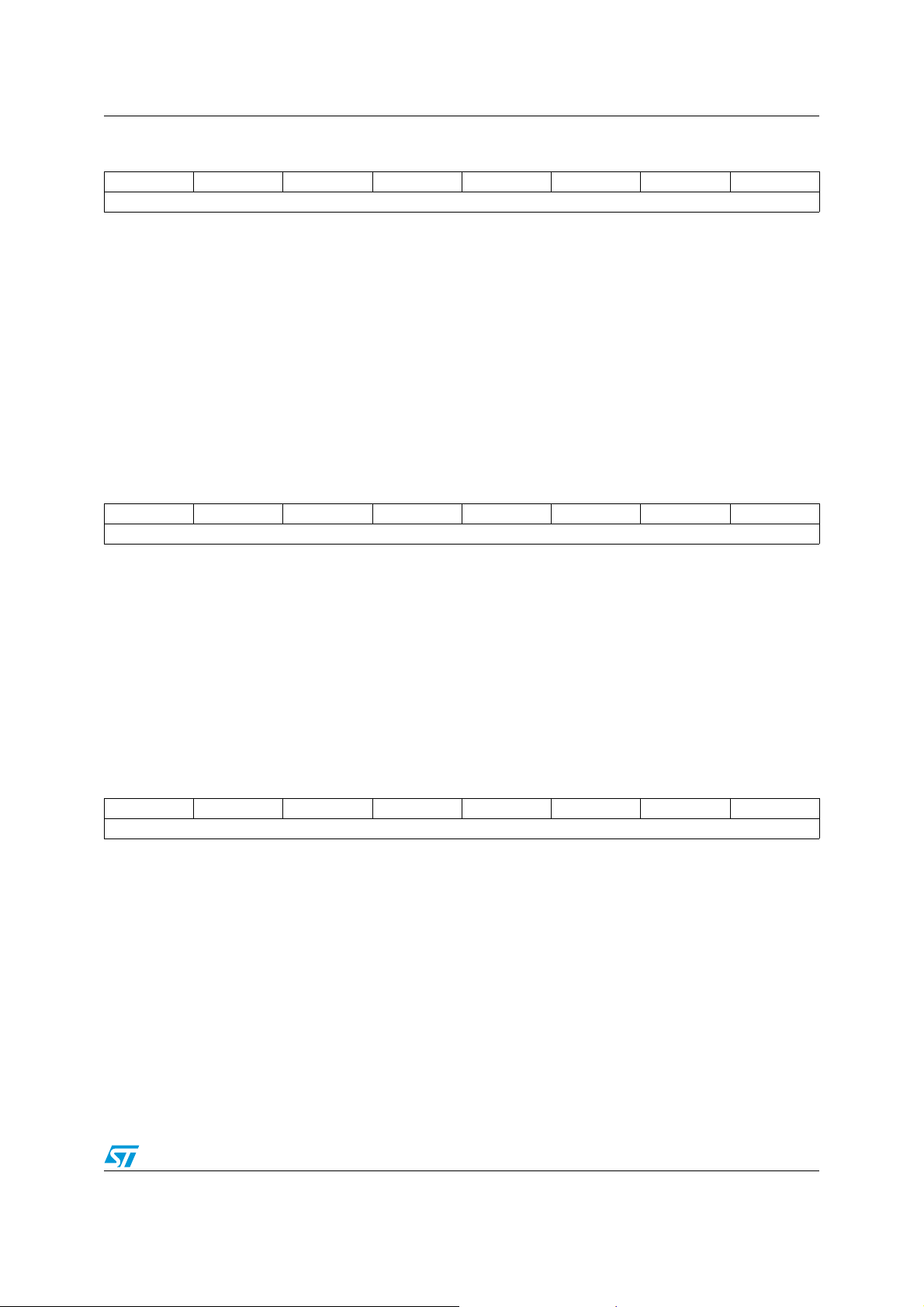
TTF1 Tri-state time after fault (LSBs)
Bit 7 Bit 6 Bit 5 Bit 4 Bit 3 Bit 2 Bit 1 Bit 0
TIM_TS_FAULT[7:0]
Address: 0x06
Type: R/W
Buffer: No
Reset: 0x02
Description:
7:0 LSBs of TIM_TS_FAULT[15:0]: time in which power is held in tristate mode after a fault
signal:
Time is TIM_TS_FAULT * 83.33 µs.
Default value (0x0002) corresponds to 166.66 µs tristate time after fault
TTP0 Tri-state time after power-up (MSBs)
Bit 7 Bit 6 Bit 5 Bit 4 Bit 3 Bit 2 Bit 1 Bit 0
TIM_TS_POWUP[15:8]
Address: 0x07
Type: R/W
Buffer: No
Reset: 0x00
Description:
7:0 MSBs of TIM_TS_POWUP[15:0]:
See register TTP1 below.
TTP1 Tristate time after power-up (LSBs)
Bit 7 Bit 6 Bit 5 Bit 4 Bit 3 Bit 2 Bit 1 Bit 0
TIM_TS_POWUP[7:0]
Address: 0x08
Type: R/W
Buffer: No
Reset: 0x02
Description:
7:0 LSBs of TIM_TS_POWUP[15:0]: time in which power is held in tri-state mode after a
power-up signal:
Time is TIM_TS_POWUP * 83.33 µs
Default value (0x0002) corresponds to 166.66 µs tristate time after power-up
Doc ID 13095 Rev 3 41/57
Page 42

Registers STA529
S2PCFG0 Serial to parallel audio interface configuration
Bit 7 Bit 6 Bit 5 Bit 4 Bit 3 Bit 2 Bit 1 Bit 0
BICLK_STRB LRCLK_LEFT SHARE_BILR MSB_FIRST DATA_FORMAT[2:0]
Address: 0x0A
Type: R/W
Buffer: No
Reset: 0xD2
Description:
7 BICLK_STRB:
0: bit clock strobe edge is falling edge, bit clock active edge is rising edge
1: bit clock strobe edge is rising edge, bit clock active edge is falling edge (default)
6 LRCLK_LEFT:
0: left/right clock is low for left channel, high for right channel
1: left/right clock is high for left channel, low for right channel (default)
5 SHARE_BILR:
0: default
1: left/right clock and bit clock are shared between serial to parallel interface and parallel to
serial interface, BICLKI and LRCLKI are used
MASTER_
MODE
4 MSB_FIRST:
0: LSB first
1: MSB first (default)
3:1 DATA_FORMAT[2:0]: serial interface protocol format:
000: left Justified
2
S (default)
001: I
010: right justified
100: PCM no delay
101: PCM delay
111: DSP
0 MASTER_MODE:
0: SAI OUTis in slave mode (default)
1: SAI OUTis in master mode
42/57 Doc ID 13095 Rev 3
Page 43

STA529 Registers
S2PCFG1 Serial-to-parallel audio interface configuration
Bit 7 Bit 6 Bit 5 Bit 4 Bit 3 Bit 2 Bit 1 Bit 0
PDATA_LENGTH[1:0] BICLK_OS[1:0] MAP_L[1:0] MAP_R[1:0]
Address: 0x0B
Type: R/W
Buffer: No
Reset: 0x91
Description:
7:6 PDATA_LENGTH[1:0]: serial-to-parallel interface data length:
Length is (N+1) * 8 bit
Default (10) is 24 bit
5:4 BICLK_OS[1:0]: bit clock oversampling:
Value is (N+1) * 32 * fs (where fs = sampling frequency)
Default (01) is 64 fs
3:2 MAP_L[1:0]: left data-mapping slot:
Value is nth slot
Default (00) is slot 0
1:0 MAP_R[1:0]: right data-mapping slot:
Value is nth slot
Default (01) is slot 1
Doc ID 13095 Rev 3 43/57
Page 44

Registers STA529
P2SCFG0 Parallel-to-serial audio interface configuration
Bit 7 Bit 6 Bit 5 Bit 4 Bit 3 Bit 2 Bit 1 Bit 0
BICLK_ STRB LRCLK_LEFT SDATAO_ACT MSB_FIRST DATA_FORMAT[2:0]
Address: 0x0C
Type: R/W
Buffer: No
Reset: 0xD3
Description:
7 BICLK_STRB: defines the bit clock edges:
0: strobe is falling edge, active edge is rising
1: strobe is rising edge, active edge is falling (default)
6 LRCLK_LEFT: defines the channel for the LR clock:
0: clock is low for left channel, high for right channel
1: clock is high for left channel, low for right channel (default)
5 SDATAO_ ACT: sets the behavior of pin SDATAO:
0: output is tristated when no data is sent (default)
1: output is never in tri-state (it is 0 when no data is sent)
4 MSB_FIRST: data alignment in the protocol for SDATAI and SDATAO:
0: LSB is the first bit
1: MSB is the first bit (default)
3:1 DATA_FORMAT[2:0]: serial interface protocol format:
000: left justified
2
S (default)
001: I
010: right justified
100: PCM no delay
101: PCM delay
111: DSP
0 MASTER_ MODE: selects serial interface master/slave mode:
0: slave
1: master (default)
MASTER_
MODE
44/57 Doc ID 13095 Rev 3
Page 45
STA529 Registers
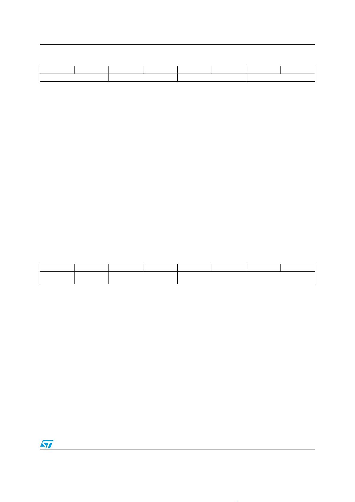
P2SCFG1 Parallel-to-serial audio interface configuration
Bit 7 Bit 6 Bit 5 Bit 4 Bit 3 Bit 2 Bit 1 Bit 0
PDATA_LENGTH[1:0] BICLK_OS[1:0] MAP_L[1:0] MAP_R[1:0]
Address: 0x0D
Type: R/W
Buffer: No
Reset: 0x91
Description:
7:6 PDATA_LENGTH[1:0]: serial-to-parallel interface data length:
Length is (PDATA_LENGTH+1) * 8 bit
Default (10) is 24 bits
5:4 BICLK_OS[1:0]: bit clock oversampling:
Value is (BICLK_OS+1) * 32 * fs
Default (01) is 64 fs
3:2 MAP_L[1:0]: left data-mapping slot:
Value is nth slot
Default (00) is slot0
1:0 MAP_R[1:0]: right channel data-mapping slot:
Value is nth slot
Default (01) is slot1
PLLCFG0 PLL configuration
Bit 7 Bit 6 Bit 5 Bit 4 Bit 3 Bit 2 Bit 1 Bit 0
PLL_DIRECT_
PROG
Address: 0x14
Type: R/W
Buffer: No
Reset: 0x00
Description:
FRAC_CTRL DITHER_DISABLE[1:0] IDF[3:0]
7 PLL_DIRECT_PROG: PLL programming:
0: default
1: PLL is programmed according to the PLLCFG register settings
Doc ID 13095 Rev 3 45/57
Page 46
Registers STA529
6 FRAC_CTRL:
0: default
1: PLL fractional-frequency synthesis is enabled
5:4 DITHER_DISABLE[1:0]:
00: default
1x: disables rectangular phase frequency divider dither input to fractional control
x1: disables triangular Phase Frequency Divider dither input to Fractional Control
The mentioned blocks are shown in Figure 5.
3:0 IDF[3:0]: PLL input division factor:
0000: IDF = 1 (default)
0001: IDF = 1
0010: IDF = 2
…
1111: IDF = 15
PLLCFG1 PLL configuration (MSBs)
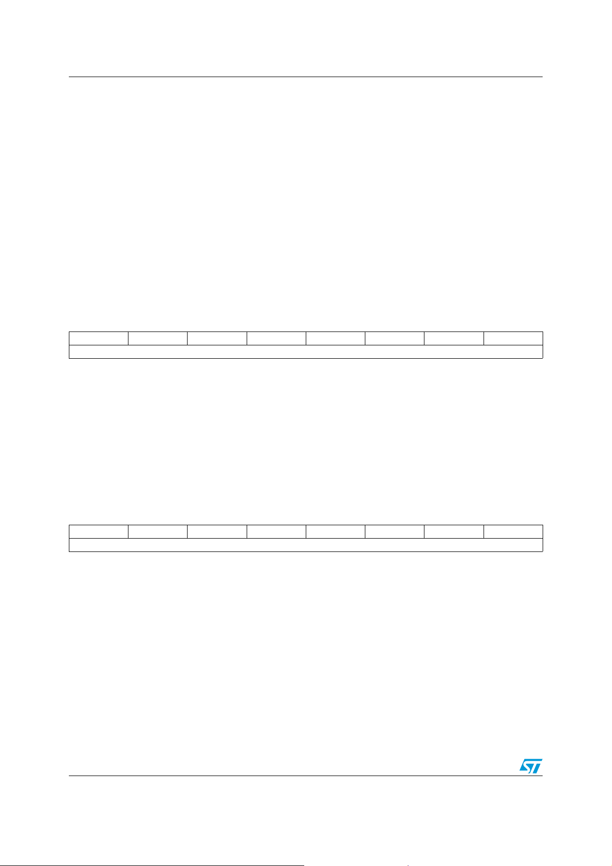
Bit 7 Bit 6 Bit 5 Bit 4 Bit 3 Bit 2 Bit 1 Bit 0
FRAC_INPUT[15:8]
Address: 0x15
Type: R/W
Buffer: No
Reset: 0x00
Description:
7:0 FRAC_INPUT[15:8]: MSBs of FRAC_INPUT[15:0] used to set the fractional part of PLL
multiplication factor
PLLCFG2 PLL configuration (LSBs)
Bit 7 Bit 6 Bit 5 Bit 4 Bit 3 Bit 2 Bit 1 Bit 0
FRAC_INPUT[7:0]
Address: 0x16
Type: R/W
Buffer: No
Reset: 0x00
Description:
7:0 FRAC_INPUT[7:0]: LSBs of FRAC_INPUT[15:0] used to set the fractional part of PLL
multiplication factor
46/57 Doc ID 13095 Rev 3
Page 47
STA529 Registers
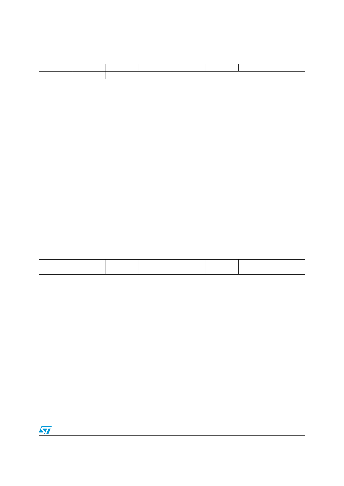
PLLCFG3 PLL configuration
Bit 7 Bit 6 Bit 5 Bit 4 Bit 3 Bit 2 Bit 1 Bit 0
STRB STRB_BYPASS NDIV[5:0]
Address: 0x17
Type: R/W
Buffer: No
Reset: 0x00
Description:
7 STRB: asynchronous strobe input to the fractional controller:
0: default
6 STRB_BYPASS: standby bypass:
0: STRB signal is not bypassed (default)
1: STRB signal is bypassed
5:0 NDIV[5:0]: PLL multiplication factor (integral part) named as loop division factor:
0000 XX: LDF = NA
0001 00: LDF = NA
0001 01: LDF = 5
...
1101 11: LDF = 55
111X XX: LDF = NA
0000 00: default
PLLPFE PLL/POP-free configuration
Bit 7 Bit 6 Bit 5 Bit 4 Bit 3 Bit 2 Bit 1 Bit 0
PLL_BYP_UNL BICLK2PLL PLL_PWDN PFE1A PFE1B PFE2A PFE2B RESET_FAULT
Address: 0x18
Type: R/W
Buffer: No
Reset: 0x00
Description:
7 PLL_BYP_UNL: PLL bypass:
0: PLL is not bypassed (default)
1: PLL is bypassed when not locked
6 BICLK2PLL:
0: default
1: BICLKI is input to PLL
5 PLL_PWDN:
0: default
1: PLL is in power-down mode
Doc ID 13095 Rev 3 47/57
Page 48
Registers STA529
4PFE1A:
0: default
1: POP-free resistances are connected to output 1A
3PFE1B:
0: default
1: POP-free resistances are connected to output 1B
2PFE2A:
0: default
1: POP-free resistances are connected to output 2A
1PFE2B:
0: default
1: POP-free resistances are connected to output 2B
0 RESET_FAULT:
0: default
1: fault signal in the I
2
C register POWST is reset
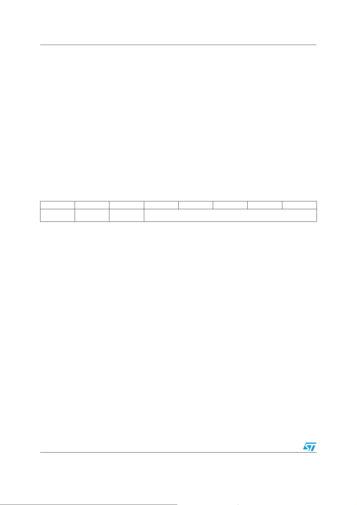
PLLST PLL status
Bit 7 Bit 6 Bit 5 Bit 4 Bit 3 Bit 2 Bit 1 Bit 0
PLL_UNLOCK
PLL_PWD_
STATE
PLL_BYP_
STATE
Reserved
Address: 0x19
Type: RO
Buffer: No
Reset: Undefined
Description:
7 PLL_UNLOCK: PLL unlock state:
0: PLL is not in unlock state
1: PLL is in unlock state
6 PLL_PWD_ STATE: PLL power-down state:
0: PLL is not in power-down state
1: PLL is in power-down state
5 PLL_BYP_STATE: PLL bypass state:
0: PLL is not in bypass state
1: PLL is in bypass state
4:0 Reserved
48/57 Doc ID 13095 Rev 3
Page 49
STA529 Registers
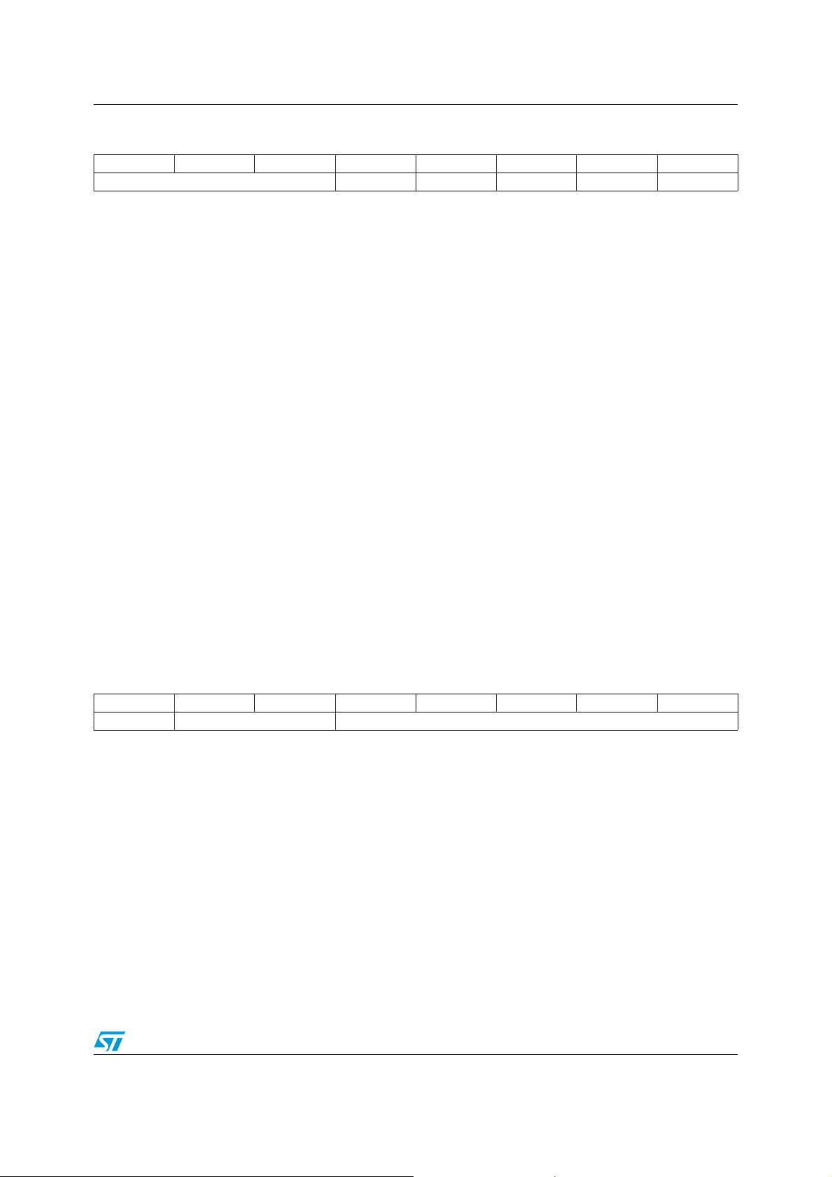
ADCCFG ADC configuration
Bit 7 Bit 6 Bit 5 Bit 4 Bit 3 Bit 2 Bit 1 Bit 0
PGA[2:0] INSEL STBY BYPASS_CALIB CLKENBL Reserved
Address: 0x1E
Type: RO
Buffer: No
Reset: Undefined
Description:
7:5 PGA[2:0]: gain selection bits for the ADC programmable gain amplifier:
000: default
Values are from 0 to 42 dB in 6 dB steps
4 INSEL:
0: line input selected (default)
1: microphone input selected (it must be applied to INL line)
3 STBY: ADC standby mode:
0: ADC in power-up mode (default)
1: ADC in standby mode
2 BYPASS_CALIB:
0: ADC DC-removal block not bypassed (default)
1: ADC DC-removal block bypassed
1 CLKENBL: Clock enable:
0: system clock not enabled
1: system clock available at ADC input (default)
0Reserved
CKOCFG Output clock configuration
Bit 7 Bit 6 Bit 5 Bit 4 Bit 3 Bit 2 Bit 1 Bit 0
CLKOUT_DIS CLKOUT_SEL[1:]] Reserved
Address: 0x1F
Type: R/W
Buffer: No
Reset: Undefined
Description:
7 CLKOUT_DIS: CLKOUT PAD disabled
0: default
1: enabled
6:5 CLKOUT_SEL[1:0]:
00: default
The CLKOUT output frequency is the PLL output frequency divided by 2
4:0 Reserved
CLKOUT_SEL
Doc ID 13095 Rev 3 49/57
Page 50
Registers STA529
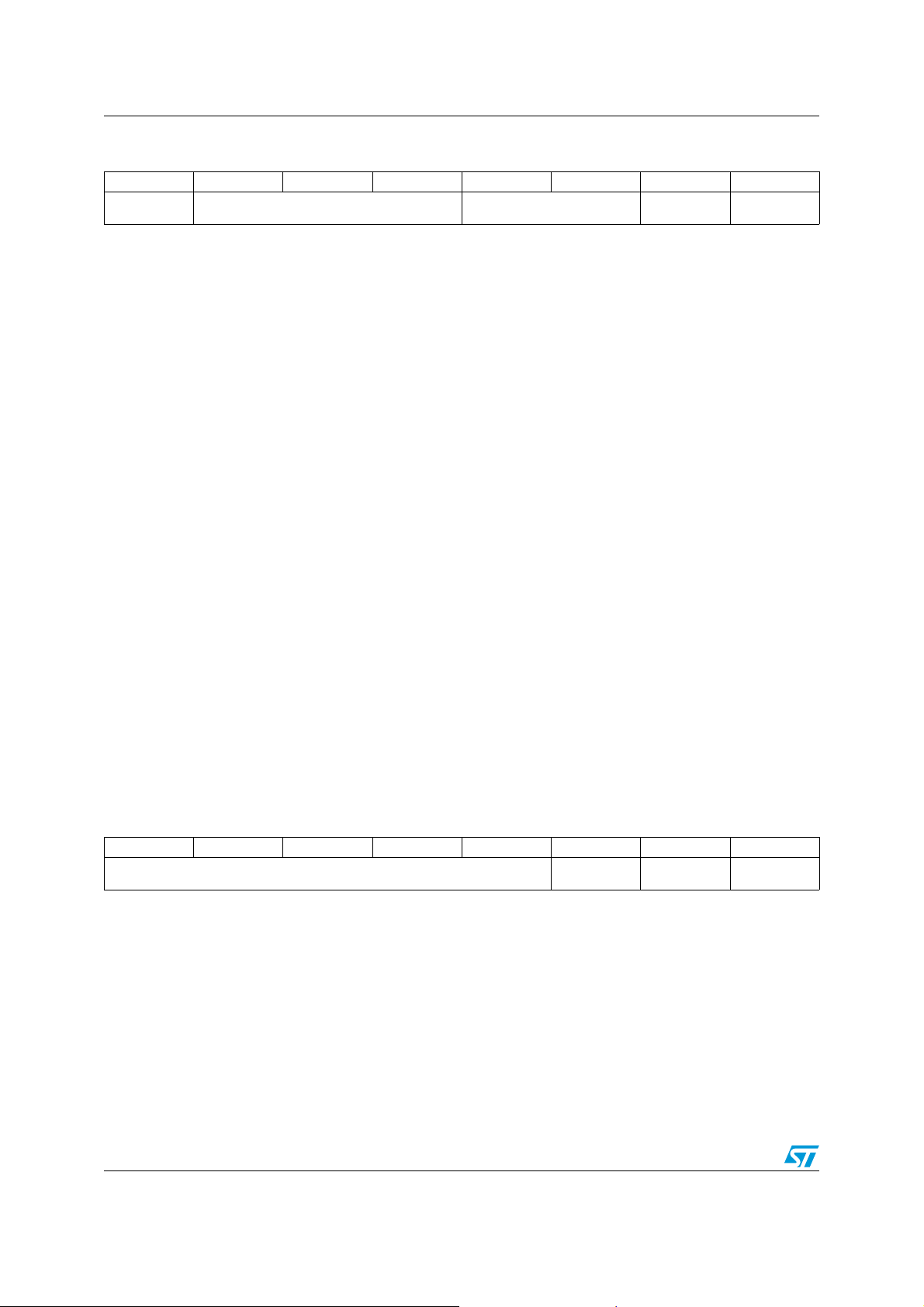
MISC Miscellaneous configuration
Bit 7 Bit 6 Bit 5 Bit 4 Bit 3 Bit 2 Bit 1 Bit 0
OSC_DIS P2P_FS_RANGE[2:0] ADC_FS_RANGE[1:0] P2P_IN_ADC
Address: 0x20
Type: R/W
Buffer: No
Reset: 0x20
Description:
7 OSC_DIS: enable/disable crystal oscillator:
0: default
1: disabled
6:4 P2P_FS_RANGE[2:0]: FFX audio frequency range:
000: very low (fs = 8 to 12 kHz)
001: low (fs = 16 to 24 kHz)
010: normal (fs = 32 to 48 kHz) (default)
011: high (fs = 64 to 96 kHz)
1X: very high (fs = 128 to 192 kHz)
3:2 ADC_FS_RANGE[2:0]: ADC audio frequency range:
00: normal (fs = 32 to 48 kHz) (default)
01: low (fs = 16 to 24 kHz)
1X: very low (fs = 8 to 12 kHz)
CORE_
CLKENBL
1 P2P_IN_ADC: FFX input:
0: FFX input is from serial-to-parallel audio interface (default)
1: FFX input is from ADC
0 CORE_CLKENBL: availability of system clock:
0: FFX system clock disabled (default)
1: FFX system clock enabled
FFXST FFX status
Bit 7 Bit 6 Bit 5 Bit 4 Bit 3 Bit 2 Bit 1 Bit 0
Reserved
Address: 0x23
Type: RO
Buffer: No
Reset: Undefined
INVALID_INP_
FBK
MUTE_INT_FBK Reserved
50/57 Doc ID 13095 Rev 3
Page 51
STA529 Registers
Description:
7:3 Reserved
2 INVALID_INP_FBK: invalid input status:
1: invalid input sent to FFX
1 MUTE_INT_FBK: FFX mute status
1: FFX is in mute state
0 Reserved
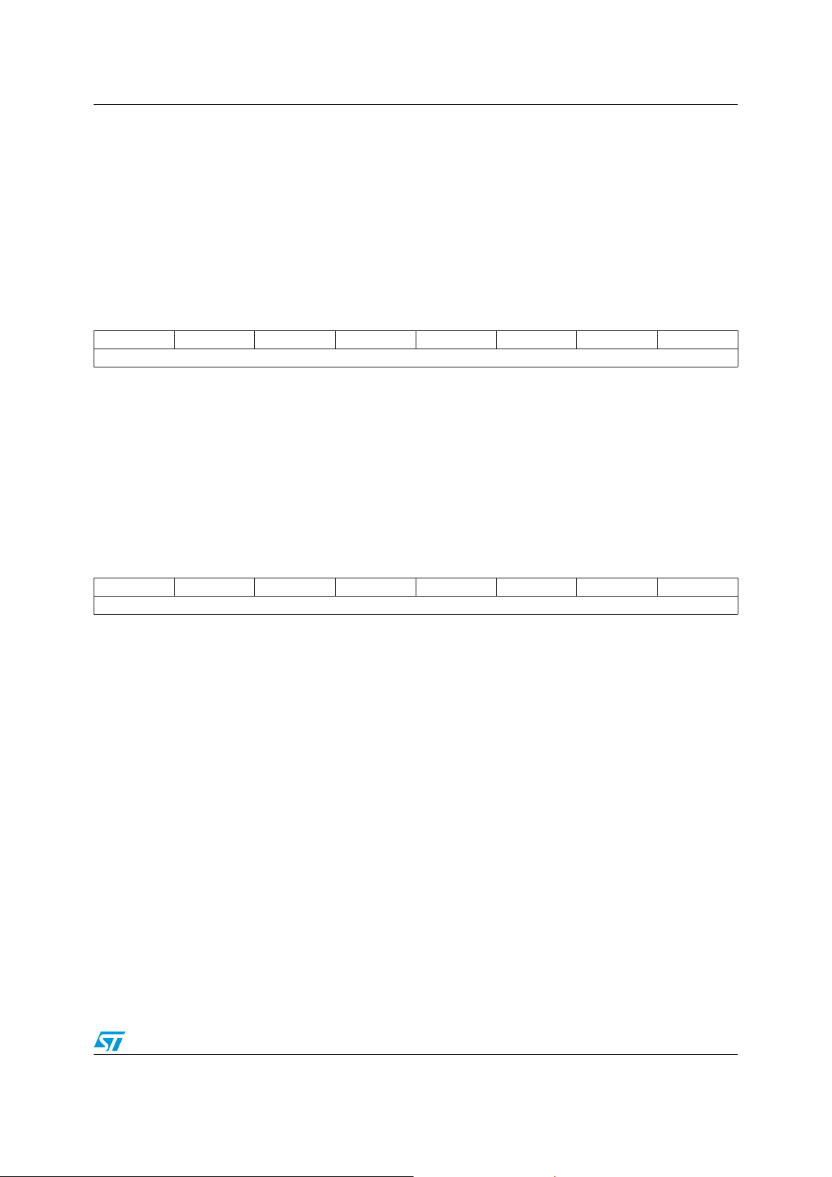
PWMINT1 PWM driver configuration (MSBs)
Bit 7 Bit 6 Bit 5 Bit 4 Bit 3 Bit 2 Bit 1 Bit 0
PWM_INT[15:8]
Address: 0x2D
Type: R/W
Buffer: No
Reset: 0x00
Description:
7:0 PWM_INT[15:8]: MSBs of PWM_INT[15:0], see Chapter 8: Driver configuration on page 28
PWMINT2 PWM driver configuration (LSBs)
Bit 7 Bit 6 Bit 5 Bit 4 Bit 3 Bit 2 Bit 1 Bit 0
PWM_INT[7:0]
Address: 0x2E
Type: R/W
Buffer: No
Reset: 0x00
Description:
7:0 PWM_INT[7:0]: LSBs of PWM_INT[15:0], see Chapter 8: Driver configuration on page 28
Doc ID 13095 Rev 3 51/57
Page 52

Registers STA529
POWST Power bridge status register
Bit 7 Bit 6 Bit 5 Bit 4 Bit 3 Bit 2 Bit 1 Bit 0
POW_
POWERDOWN
Address: 0x32
Type: RO
Buffer: No
Reset: Undefined
Description:
POW_
TRISTATE
POW_FAULT1A POW_FAULT1B POW_FAULT2A POW_FAULT2B Reserved
7 POW_POWERDOWN: power-down bridge:
0: not in power-down state
1: power-down state
6 POW_TRISTATE:
1: power bridge is in tristate
5POW_FAULT1A:
1: power bridge 1A is in fault state
4POW_FAULT1B:
1: power bridge 1B is in fault state
3POW_FAULT2A:
1: power bridge 2A is in fault state
2POW_FAULT2B:
1: power bridge 2B is in fault state
1:0 Reserved
52/57 Doc ID 13095 Rev 3
Page 53
STA529 Package mechanical data
12 Package mechanical data
This section contains packaging information for the following packages:
● TFBGA48
● VFQFPN52
In order to meet environmental requirements, ST offers these devices in different grades of
ECOPACK
specifications, grade definitions and product status are available at: www.st.com.
ECOPACK
®
packages, depending on their level of environmental compliance. ECOPACK®
®
is an ST trademark.
12.1 Package TFBGA48
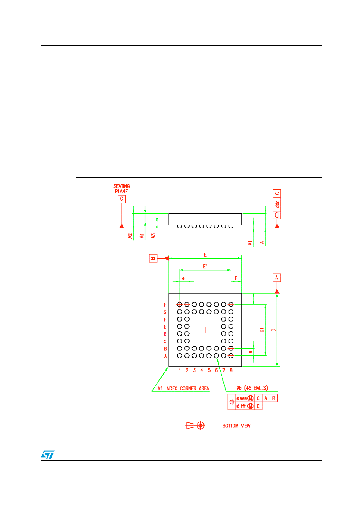
Figure 18. Package outline (TFBGA48)
Doc ID 13095 Rev 3 53/57
Page 54
Package mechanical data STA529
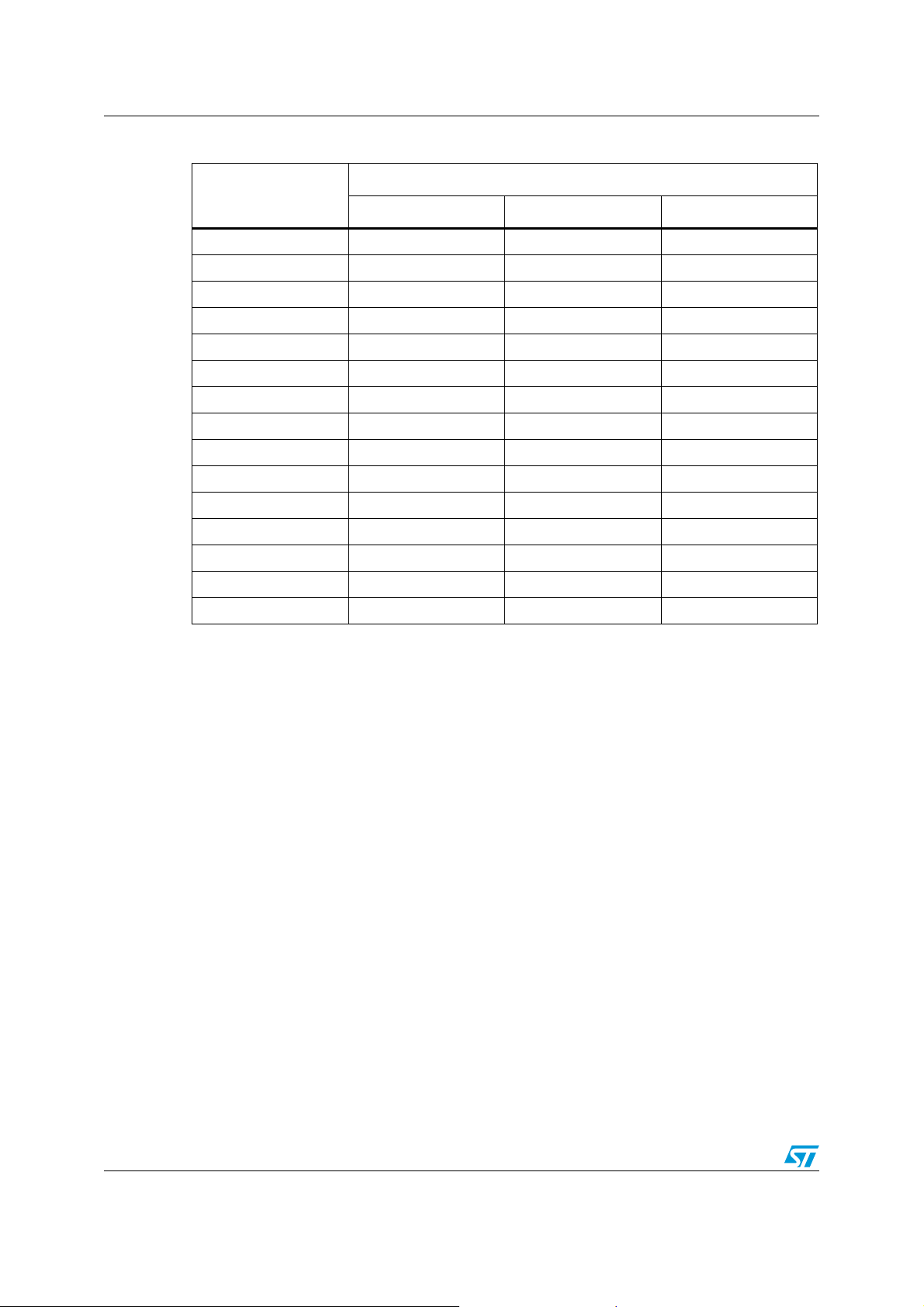
Table 23. Package dimensions (TFBGA48)
Dimensions in mm
Reference
Min Typ Max
A--1.20
A1 0.15 - -
A2 - 0.785 -
A3 - 0.20 -
A4--0.60
b 0.25 0.30 0.35
D 4.85 5.00 5.15
D1 - 3.50 -
E 4.85 5.00 5.15
E1 - 3.50 -
e - 0.50 -
F - 0.75 -
ddd - - 0.08
eee - - 0.15
fff - - 0.05
54/57 Doc ID 13095 Rev 3
Page 55
STA529 Package mechanical data
12.2 Package VFQFPN52
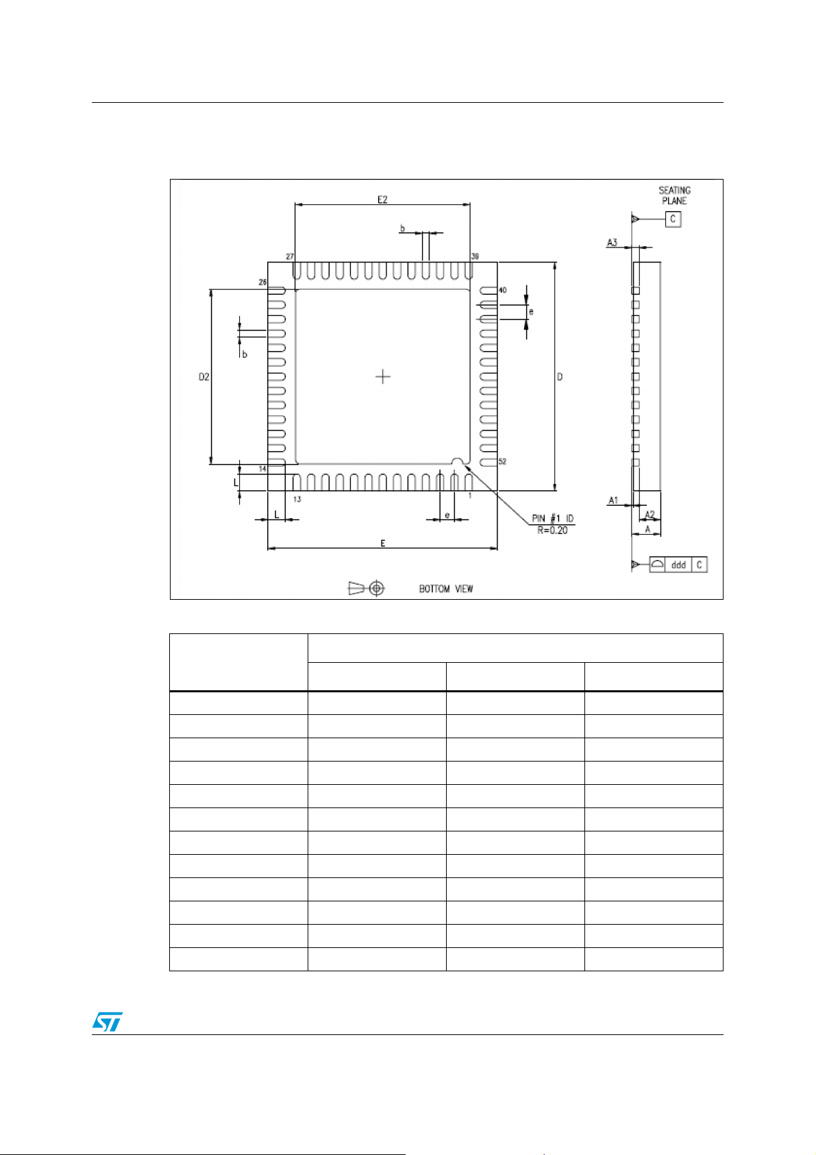
Figure 19. Package outline (VFQFPN52)
Table 24. Package dimensions (VFQFPN52)
Dimensions in mm
Reference
Min Typ Max
A 0.800 0.900 1.000
A1 - 0.020 0.050
A2 - 0.650 1.000
A3 - 0.250 -
b 0.180 0.230 0.300
D 7.875 8.000 8.125
D2 2.750 5.700 6.250
E 7.875 8.000 8.125
E2 2.750 5.700 6.250
e 0.450 0.500 0.550
L 0.350 0.550 0.750
ddd - - 0.080
Doc ID 13095 Rev 3 55/57
Page 56
Revision history STA529
13 Revision history
Table 25. Document revision history
Date Revision Changes
25-Jan-2007 1 Initial release.
09-Apr-2010 2 Complete update and change in presentation
Updated Features
30-Mar-2012 3
Added Section 6.3: Set fractional PLL
Updated Section 7.2: Functional description
Minor textual updates
56/57 Doc ID 13095 Rev 3
Page 57

STA529
Please Read Carefully:
Information in this document is provided solely in connection with ST products. STMicroelectronics NV and its subsidiaries (“ST”) reserve the
right to make changes, corrections, modifications or improvements, to this document, and the products and services described herein at any
time, without notice.
All ST products are sold pursuant to ST’s terms and conditions of sale.
Purchasers are solely responsible for the choice, selection and use of the ST products and services described herein, and ST assumes no
liability whatsoever relating to the choice, selection or use of the ST products and services described herein.
No license, express or implied, by estoppel or otherwise, to any intellectual property rights is granted under this document. If any part of this
document refers to any third party products or services it shall not be deemed a license grant by ST for the use of such third party products
or services, or any intellectual property contained therein or considered as a warranty covering the use in any manner whatsoever of such
third party products or services or any intellectual property contained therein.
UNLESS OTHERWISE SET FORTH IN ST’S TERMS AND CONDITIONS OF SALE ST DISCLAIMS ANY EXPRESS OR IMPLIED
WARRANTY WITH RESPECT TO THE USE AND/OR SALE OF ST PRODUCTS INCLUDING WITHOUT LIMITATION IMPLIED
WARRANTIES OF MERCHANTABILITY, FITNESS FOR A PARTICULAR PURPOSE (AND THEIR EQUIVALENTS UNDER THE LAWS
OF ANY JURISDICTION), OR INFRINGEMENT OF ANY PATENT, COPYRIGHT OR OTHER INTELLECTUAL PROPERTY RIGHT.
UNLESS EXPRESSLY APPROVED IN WRITING BY TWO AUTHORIZED ST REPRESENTATIVES, ST PRODUCTS ARE NOT
RECOMMENDED, AUTHORIZED OR WARRANTED FOR USE IN MILITARY, AIR CRAFT, SPACE, LIFE SAVING, OR LIFE SUSTAINING
APPLICATIONS, NOR IN PRODUCTS OR SYSTEMS WHERE FAILURE OR MALFUNCTION MAY RESULT IN PERSONAL INJURY,
DEATH, OR SEVERE PROPERTY OR ENVIRONMENTAL DAMAGE. ST PRODUCTS WHICH ARE NOT SPECIFIED AS "AUTOMOTIVE
GRADE" MAY ONLY BE USED IN AUTOMOTIVE APPLICATIONS AT USER’S OWN RISK.
Resale of ST products with provisions different from the statements and/or technical features set forth in this document shall immediately void
any warranty granted by ST for the ST product or service described herein and shall not create or extend in any manner whatsoever, any
liability of ST.
ST and the ST logo are trademarks or registered trademarks of ST in various countries.
Information in this document supersedes and replaces all information previously supplied.
The ST logo is a registered trademark of STMicroelectronics. All other names are the property of their respective owners.
© 2012 STMicroelectronics - All rights reserved
STMicroelectronics group of companies
Australia - Belgium - Brazil - Canada - China - Czech Republic - Finland - France - Germany - Hong Kong - India - Israel - Italy - Japan -
Malaysia - Malta - Morocco - Philippines - Singapore - Spain - Sweden - Switzerland - United Kingdom - United States of America
www.st.com
Doc ID 13095 Rev 3 57/57
 Loading...