

2.1-channel 40-watt high-efficiency digital audio system
Features
Wide-range supply voltage, 4.5 V to 21.5 V
Three power output configurations:
– 2 channels of ternary PWM
(2 x 20 W into 8 Ω at 18 V) + PWM output
– 2 channels of ternary PWM
(2 x 20 W into 8 Ω at 18 V) + ternary stereo
line-out
– 2.1 channels of binary PWM (left, right,
LFE) (2 x 9 W into 4 Ω +1 x 20 W into 8 Ω
at 18 V)
FFX with 100-dB SNR and dynamic range
Scalable FFX modulation index (up to 100%)
Selectable 32- to 192-kHz input sample rates
2
I
C control with selectable device address
Digital gain/attenuation +48 dB to -80 dB with
0.125-dB/step resolution
Soft volume update with programmable ratio
Individual channel and master gain/attenuation
Two independent DRCs configurable as a
dual-band anti-clipper (B
independent limiters/compressors with
optional global DRC capability
EQ-DRC for DRC based on filtered signals
Dedicated LFE processing for bass boosting
with 0.125-dB/step resolution
Audio presets:
– 15 preset crossover filters
– 5 preset anti-clipping modes
– Preset night-time listening mode
Individual channel soft/hard mute
Independent channel volume and DSP bypass
2
I
S input data interface
Input and output channel mapping
2
DRC) or as
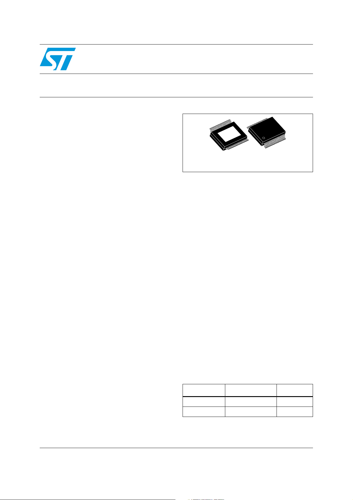
STA369BWS
Sound Terminal™
PowerSSO-36
with exposed pad down (EPD)
Automatic invalid input-detect mute
Up to 8 user-programmable biquads/channel
Three coefficients banks for EQ presets storing
with fast recall via I
Extended filter dynamics +4/-4 for better sound
shaping and easier filter implementation
Bass/treble tones and de-emphasis control
Selectable high-pass filter for DC blocking
Advanced AM interference frequency
switching and noise suppression modes
F3X™ advanced PWM modulation scheme for
carrier suppression (headphone or line output)
Selectable high- or low-bandwidth
noise-shaping topologies
Selectable clock input ratio
96-kHz internal processing sample rate with
quantization error noise shaping for very low
cut-off frequency filters
Thermal overload and short-circuit protection
embedded
Video apps: 576 x f
PCB manufacturing short-circuit protection
technology
Table 1. Device summary
Order code Package Packaging
STA369BWS PowerSSO-36 EPD Tube
STA369BWSTR PowerSSO-36 EPD Tape and reel
2
C interface
input mode supported
S
November 2010 Doc ID 16861 Rev 4 1/89
www.st.com
89

Contents STA369BWS
Contents
1 Description . . . . . . . . . . . . . . . . . . . . . . . . . . . . . . . . . . . . . . . . . . . . . . . . . 9
2 Pin connections . . . . . . . . . . . . . . . . . . . . . . . . . . . . . . . . . . . . . . . . . . . . 11
2.1 Connection diagram . . . . . . . . . . . . . . . . . . . . . . . . . . . . . . . . . . . . . . . . . 11
2.2 Pin description . . . . . . . . . . . . . . . . . . . . . . . . . . . . . . . . . . . . . . . . . . . . . 11
3 Electrical specifications . . . . . . . . . . . . . . . . . . . . . . . . . . . . . . . . . . . . . 13
3.1 Absolute maximum ratings . . . . . . . . . . . . . . . . . . . . . . . . . . . . . . . . . . . . 13
3.2 Thermal data . . . . . . . . . . . . . . . . . . . . . . . . . . . . . . . . . . . . . . . . . . . . . . 13
3.3 Recommended operating conditions . . . . . . . . . . . . . . . . . . . . . . . . . . . . 14
3.4 Electrical specifications for the digital section . . . . . . . . . . . . . . . . . . . . . 14
3.5 Electrical specifications for the power section . . . . . . . . . . . . . . . . . . . . . 15
3.6 Power on/off sequence . . . . . . . . . . . . . . . . . . . . . . . . . . . . . . . . . . . . . . . 17
4 Processing data paths . . . . . . . . . . . . . . . . . . . . . . . . . . . . . . . . . . . . . . 18
5I
2
C bus specification . . . . . . . . . . . . . . . . . . . . . . . . . . . . . . . . . . . . . . . . 20
5.1 Communication protocol . . . . . . . . . . . . . . . . . . . . . . . . . . . . . . . . . . . . . . 20
5.1.1 Data transition or change . . . . . . . . . . . . . . . . . . . . . . . . . . . . . . . . . . . . 20
5.1.2 Start condition . . . . . . . . . . . . . . . . . . . . . . . . . . . . . . . . . . . . . . . . . . . . 20
5.1.3 Stop condition . . . . . . . . . . . . . . . . . . . . . . . . . . . . . . . . . . . . . . . . . . . . 20
5.1.4 Data input . . . . . . . . . . . . . . . . . . . . . . . . . . . . . . . . . . . . . . . . . . . . . . . 20
5.2 Device addressing . . . . . . . . . . . . . . . . . . . . . . . . . . . . . . . . . . . . . . . . . . 20
5.3 Write operation . . . . . . . . . . . . . . . . . . . . . . . . . . . . . . . . . . . . . . . . . . . . . 21
5.3.1 Byte write . . . . . . . . . . . . . . . . . . . . . . . . . . . . . . . . . . . . . . . . . . . . . . . . 21
5.3.2 Multi-byte write . . . . . . . . . . . . . . . . . . . . . . . . . . . . . . . . . . . . . . . . . . . . 21
5.4 Read operation . . . . . . . . . . . . . . . . . . . . . . . . . . . . . . . . . . . . . . . . . . . . . 21
5.4.1 Current address byte read . . . . . . . . . . . . . . . . . . . . . . . . . . . . . . . . . . . 21
5.4.2 Current address multi-byte read . . . . . . . . . . . . . . . . . . . . . . . . . . . . . . 21
5.4.3 Random address byte read . . . . . . . . . . . . . . . . . . . . . . . . . . . . . . . . . . 21
5.4.4 Random address multi-byte read . . . . . . . . . . . . . . . . . . . . . . . . . . . . . . 22
6 Register description . . . . . . . . . . . . . . . . . . . . . . . . . . . . . . . . . . . . . . . . 23
2/89 Doc ID 16861 Rev 4

STA369BWS Contents
6.1 Configuration registers (addr 0x00 to 0x05) . . . . . . . . . . . . . . . . . . . . . . . 26
6.1.1 Configuration register A (addr 0x00) . . . . . . . . . . . . . . . . . . . . . . . . . . . 26
6.1.2 Configuration register B (addr 0x01) . . . . . . . . . . . . . . . . . . . . . . . . . . . 28
6.1.3 Configuration register C (addr 0x02) . . . . . . . . . . . . . . . . . . . . . . . . . . . 31
6.1.4 Configuration register D (addr 0x03) . . . . . . . . . . . . . . . . . . . . . . . . . . . 32
6.1.5 Configuration register E (addr 0x04) . . . . . . . . . . . . . . . . . . . . . . . . . . . 34
6.1.6 Configuration register F (addr 0x05) . . . . . . . . . . . . . . . . . . . . . . . . . . . 36
6.2 Volume control registers (addr 0x06 - 0x0A) . . . . . . . . . . . . . . . . . . . . . . 44
6.2.1 Mute/line output configuration register (addr 0x06) . . . . . . . . . . . . . . . . 45
6.2.2 Master volume register (addr 0x07) . . . . . . . . . . . . . . . . . . . . . . . . . . . . 45
6.2.3 Channel 1 volume (addr 0x08) . . . . . . . . . . . . . . . . . . . . . . . . . . . . . . . . 45
6.2.4 Channel 2 volume (addr 0x09) . . . . . . . . . . . . . . . . . . . . . . . . . . . . . . . . 45
6.2.5 Channel 3 / line output volume (addr 0x0A) . . . . . . . . . . . . . . . . . . . . . . 46
6.3 Audio preset registers (addr 0x0B and 0x0C) . . . . . . . . . . . . . . . . . . . . . 47
6.3.1 Audio preset register 1 (addr 0x0B) . . . . . . . . . . . . . . . . . . . . . . . . . . . . 47
6.3.2 Audio preset register 2 (addr 0x0C) . . . . . . . . . . . . . . . . . . . . . . . . . . . . 47
6.4 Channel configuration registers (addr 0x0E - 0x10) . . . . . . . . . . . . . . . . . 49
6.5 Tone control register (addr 0x11) . . . . . . . . . . . . . . . . . . . . . . . . . . . . . . . 51
6.6 Dynamic control registers (addr 0x12 - 0x15) . . . . . . . . . . . . . . . . . . . . . 51
6.6.1 Limiter 1 attack/release rate (addr 0x12) . . . . . . . . . . . . . . . . . . . . . . . . 51
6.6.2 Limiter 1 attack/release threshold (addr 0x13) . . . . . . . . . . . . . . . . . . . . 51
6.6.3 Limiter 2 attack/release rate (addr 0x14) . . . . . . . . . . . . . . . . . . . . . . . . 52
6.6.4 Limiter 2 attack/release threshold (addr 0x15) . . . . . . . . . . . . . . . . . . . . 52
6.6.5 Description . . . . . . . . . . . . . . . . . . . . . . . . . . . . . . . . . . . . . . . . . . . . . . . 52
6.6.6 Limiter 1 extended attack threshold (addr 0x32) . . . . . . . . . . . . . . . . . . 56
6.6.7 Limiter 1 extended release threshold (addr 0x33) . . . . . . . . . . . . . . . . . 57
6.6.8 Limiter 2 extended attack threshold (addr 0x34) . . . . . . . . . . . . . . . . . . 57
6.6.9 Limiter 2 extended release threshold (addr 0x35) . . . . . . . . . . . . . . . . . 57
6.7 User-defined coefficient control registers (addr 0x16 - 0x26) . . . . . . . . . . 57
6.7.1 Coefficient address register (addr 0x16) . . . . . . . . . . . . . . . . . . . . . . . . 57
6.7.2 Coefficient b1 data register bits (addr 0x17 - 0x19) . . . . . . . . . . . . . . . . 57
6.7.3 Coefficient b2 data register bits (addr 0x1A - 0x1C) . . . . . . . . . . . . . . . 58
6.7.4 Coefficient a1 data register bits (addr 0x1D - 0x1F) . . . . . . . . . . . . . . . 58
6.7.5 Coefficient a2 data register bits (addr 0x20 - 0x22) . . . . . . . . . . . . . . . . 58
6.7.6 Coefficient b0 data register bits (addr 0x23 - 0x25) . . . . . . . . . . . . . . . . 59
6.7.7 Coefficient read/write control register (addr 0x26) . . . . . . . . . . . . . . . . . 59
Doc ID 16861 Rev 4 3/89

Contents STA369BWS
6.7.8 Description . . . . . . . . . . . . . . . . . . . . . . . . . . . . . . . . . . . . . . . . . . . . . . . 59
6.8 Variable max power correction registers (addr 0x27 - 0x28) . . . . . . . . . . 64
6.9 Distortion compensation registers (addr 0x29 - 0x2A) . . . . . . . . . . . . . . . 64
6.10 Fault detect recovery constant registers (addr 0x2B - 0x2C) . . . . . . . . . . 64
6.11 Device status register (addr 0x2D) . . . . . . . . . . . . . . . . . . . . . . . . . . . . . . 65
6.12 EQ coefficients and DRC configuration register (addr 0x31) . . . . . . . . . . 66
6.13 Extended configuration register (addr 0x36) . . . . . . . . . . . . . . . . . . . . . . 67
6.13.1 Dual-band DRC (B2DRC) . . . . . . . . . . . . . . . . . . . . . . . . . . . . . . . . . . . 67
6.13.2 EQ DRC mode . . . . . . . . . . . . . . . . . . . . . . . . . . . . . . . . . . . . . . . . . . . . 68
6.14 Soft volume configuration registers (addr 0x37 - 0x38) . . . . . . . . . . . . . . 70
6.15 DRC RMS filter coefficients (addr 0x39-0x3E) . . . . . . . . . . . . . . . . . . . . . 71
6.16 Extra volume resolution configuration registers (addr 0x3F) . . . . . . . . . . 72
6.17 Short-circuit protection mode registers SHOK (addr 0x46) . . . . . . . . . . . 73
6.18 Quantization error noise correction (addr 0x48) . . . . . . . . . . . . . . . . . . . . 74
6.19 Extended coefficient range up to +4/-4 (addr 0x49, 0x4A) . . . . . . . . . . . . 75
6.20 Miscellaneous registers (addr 0x4B, 0x4C) . . . . . . . . . . . . . . . . . . . . . . . 76
6.20.1 MISC1 (addr 0x4B) . . . . . . . . . . . . . . . . . . . . . . . . . . . . . . . . . . . . . . . . 76
6.20.2 MISC2 (addr 0x4C) . . . . . . . . . . . . . . . . . . . . . . . . . . . . . . . . . . . . . . . . 78
6.21 Global DRC after B2DRC (GDRC) bit (addr 0x4D, bit D0) . . . . . . . . . . . . 79
6.22 Bad PWM detection registers (addr 0x4D, 0x4E, 0x4F) . . . . . . . . . . . . . . 80
6.23 Coefficient RAM CRC protection (addr 0x60-0x6C) . . . . . . . . . . . . . . . . . 80
6.23.1 BQCHKE registers (addr 0x60 - 0x62) . . . . . . . . . . . . . . . . . . . . . . . . . 80
6.23.2 XCCHKE registers (addr 0x63 - 0x65) . . . . . . . . . . . . . . . . . . . . . . . . . . 81
6.23.3 BQCHKR registers (addr 0x66 - 0x68) . . . . . . . . . . . . . . . . . . . . . . . . . 81
6.23.4 XCCHKR registers (addr 0x69 - 0x6B) . . . . . . . . . . . . . . . . . . . . . . . . . 81
6.23.5 CHKCTRL register (addr 0x6C) . . . . . . . . . . . . . . . . . . . . . . . . . . . . . . . 81
6.23.6 Description . . . . . . . . . . . . . . . . . . . . . . . . . . . . . . . . . . . . . . . . . . . . . . . 82
7 Applications . . . . . . . . . . . . . . . . . . . . . . . . . . . . . . . . . . . . . . . . . . . . . . . 83
7.1 Applications schematic . . . . . . . . . . . . . . . . . . . . . . . . . . . . . . . . . . . . . . . 83
7.2 PLL filter circuit . . . . . . . . . . . . . . . . . . . . . . . . . . . . . . . . . . . . . . . . . . . . . 83
7.3 Typical output configuration . . . . . . . . . . . . . . . . . . . . . . . . . . . . . . . . . . . 84
8 Package thermal characteristics . . . . . . . . . . . . . . . . . . . . . . . . . . . . . . 85
4/89 Doc ID 16861 Rev 4

STA369BWS Contents
9 Package mechanical data . . . . . . . . . . . . . . . . . . . . . . . . . . . . . . . . . . . . 86
10 Revision history . . . . . . . . . . . . . . . . . . . . . . . . . . . . . . . . . . . . . . . . . . . 88
Doc ID 16861 Rev 4 5/89

List of figures STA369BWS
List of figures
Figure 1. Block diagram . . . . . . . . . . . . . . . . . . . . . . . . . . . . . . . . . . . . . . . . . . . . . . . . . . . . . . . . . . . 9
Figure 2. Pin connection PowerSSO-36 (top view) . . . . . . . . . . . . . . . . . . . . . . . . . . . . . . . . . . . . . . 11
Figure 3. Test circuit . . . . . . . . . . . . . . . . . . . . . . . . . . . . . . . . . . . . . . . . . . . . . . . . . . . . . . . . . . . . . 16
Figure 4. Power-on sequence . . . . . . . . . . . . . . . . . . . . . . . . . . . . . . . . . . . . . . . . . . . . . . . . . . . . . . 17
Figure 5. Power-off sequence for pop-free turn-off . . . . . . . . . . . . . . . . . . . . . . . . . . . . . . . . . . . . . . 17
Figure 6. Left and right processing, section 1 . . . . . . . . . . . . . . . . . . . . . . . . . . . . . . . . . . . . . . . . . . 18
Figure 7. Left and right processing, section 2 . . . . . . . . . . . . . . . . . . . . . . . . . . . . . . . . . . . . . . . . . . 19
Figure 8. Write mode sequence . . . . . . . . . . . . . . . . . . . . . . . . . . . . . . . . . . . . . . . . . . . . . . . . . . . . . 21
Figure 9. Read mode sequence. . . . . . . . . . . . . . . . . . . . . . . . . . . . . . . . . . . . . . . . . . . . . . . . . . . . . 22
Figure 10. OCFG = 00 (default value) . . . . . . . . . . . . . . . . . . . . . . . . . . . . . . . . . . . . . . . . . . . . . . . . . 37
Figure 11. OCFG = 01 . . . . . . . . . . . . . . . . . . . . . . . . . . . . . . . . . . . . . . . . . . . . . . . . . . . . . . . . . . . . 38
Figure 12. OCFG = 10 . . . . . . . . . . . . . . . . . . . . . . . . . . . . . . . . . . . . . . . . . . . . . . . . . . . . . . . . . . . . 38
Figure 13. OCFG = 11 . . . . . . . . . . . . . . . . . . . . . . . . . . . . . . . . . . . . . . . . . . . . . . . . . . . . . . . . . . . . 38
Figure 14. Output mapping scheme . . . . . . . . . . . . . . . . . . . . . . . . . . . . . . . . . . . . . . . . . . . . . . . . . . 39
Figure 15. 2.0 channels (OCFG = 00) PWM slots . . . . . . . . . . . . . . . . . . . . . . . . . . . . . . . . . . . . . . . 40
Figure 16. 2.1 channels (OCFG = 01) PWM slots . . . . . . . . . . . . . . . . . . . . . . . . . . . . . . . . . . . . . . . 41
Figure 17. 2.1 channels (OCFG = 10) PWM slots . . . . . . . . . . . . . . . . . . . . . . . . . . . . . . . . . . . . . . . 42
Figure 18. Basic limiter and volume flow diagram . . . . . . . . . . . . . . . . . . . . . . . . . . . . . . . . . . . . . . . . 52
Figure 19. B
Figure 20. EQDRC scheme . . . . . . . . . . . . . . . . . . . . . . . . . . . . . . . . . . . . . . . . . . . . . . . . . . . . . . . . 69
Figure 21. Extra resolution volume scheme . . . . . . . . . . . . . . . . . . . . . . . . . . . . . . . . . . . . . . . . . . . . 72
Figure 22. Short-circuit detection timing diagram (no short detected) . . . . . . . . . . . . . . . . . . . . . . . . 74
Figure 23. Biquad filter structure with quantization-error noise shaping . . . . . . . . . . . . . . . . . . . . . . . 75
Figure 24. External active filter with connection for F3X output . . . . . . . . . . . . . . . . . . . . . . . . . . . . . 77
Figure 25. Alternate function for INT_LINE pin . . . . . . . . . . . . . . . . . . . . . . . . . . . . . . . . . . . . . . . . . . 78
Figure 26. Global DRC after B2DRC . . . . . . . . . . . . . . . . . . . . . . . . . . . . . . . . . . . . . . . . . . . . . . . . . . 79
Figure 27. Applications circuit . . . . . . . . . . . . . . . . . . . . . . . . . . . . . . . . . . . . . . . . . . . . . . . . . . . . . . . 83
Figure 28. Output configuration for stereo BTL mode (R
Figure 29. PowerSSO-36 power derating curve . . . . . . . . . . . . . . . . . . . . . . . . . . . . . . . . . . . . . . . . . 85
Figure 30. PowerSSO-36 EPD outline drawing . . . . . . . . . . . . . . . . . . . . . . . . . . . . . . . . . . . . . . . . . 86
2
DRC scheme . . . . . . . . . . . . . . . . . . . . . . . . . . . . . . . . . . . . . . . . . . . . . . . . . . . . . . . . . 67
= 8 Ω) . . . . . . . . . . . . . . . . . . . . . . . . . . . . 84
L
6/89 Doc ID 16861 Rev 4

STA369BWS List of tables
List of tables
Table 1. Device summary . . . . . . . . . . . . . . . . . . . . . . . . . . . . . . . . . . . . . . . . . . . . . . . . . . . . . . . . . . 1
Table 2. Pin description . . . . . . . . . . . . . . . . . . . . . . . . . . . . . . . . . . . . . . . . . . . . . . . . . . . . . . . . . . 11
Table 3. Absolute maximum ratings . . . . . . . . . . . . . . . . . . . . . . . . . . . . . . . . . . . . . . . . . . . . . . . . . 13
Table 4. Thermal data. . . . . . . . . . . . . . . . . . . . . . . . . . . . . . . . . . . . . . . . . . . . . . . . . . . . . . . . . . . . 13
Table 5. Recommended operating condition . . . . . . . . . . . . . . . . . . . . . . . . . . . . . . . . . . . . . . . . . . 14
Table 6. Electrical specifications - digital section (T
Table 7. Electrical specifications - power section . . . . . . . . . . . . . . . . . . . . . . . . . . . . . . . . . . . . . . . 15
Table 8. Register summary. . . . . . . . . . . . . . . . . . . . . . . . . . . . . . . . . . . . . . . . . . . . . . . . . . . . . . . . 23
Table 9. Master clock select . . . . . . . . . . . . . . . . . . . . . . . . . . . . . . . . . . . . . . . . . . . . . . . . . . . . . . . 26
Table 10. Input sampling rates . . . . . . . . . . . . . . . . . . . . . . . . . . . . . . . . . . . . . . . . . . . . . . . . . . . . . . 26
Table 11. Internal interpolation ratio . . . . . . . . . . . . . . . . . . . . . . . . . . . . . . . . . . . . . . . . . . . . . . . . . . 26
Table 12. IR bit settings as a function of input sample rate . . . . . . . . . . . . . . . . . . . . . . . . . . . . . . . . 27
Table 13. Thermal warning recovery bypass . . . . . . . . . . . . . . . . . . . . . . . . . . . . . . . . . . . . . . . . . . . 27
Table 14. Thermal warning adjustment bypass . . . . . . . . . . . . . . . . . . . . . . . . . . . . . . . . . . . . . . . . . 27
Table 15. Fault detect recovery bypass . . . . . . . . . . . . . . . . . . . . . . . . . . . . . . . . . . . . . . . . . . . . . . . 28
Table 16. Serial audio input interface . . . . . . . . . . . . . . . . . . . . . . . . . . . . . . . . . . . . . . . . . . . . . . . . . 28
Table 17. Serial data first bit . . . . . . . . . . . . . . . . . . . . . . . . . . . . . . . . . . . . . . . . . . . . . . . . . . . . . . . . 28
Table 18. Support serial audio input formats for MSB-first (SAIFB = 0) . . . . . . . . . . . . . . . . . . . . . . . 29
Table 19. Supported serial audio input formats for LSB-first (SAIFB = 1) . . . . . . . . . . . . . . . . . . . . . 29
Table 20. Delay serial clock enable . . . . . . . . . . . . . . . . . . . . . . . . . . . . . . . . . . . . . . . . . . . . . . . . . . 30
Table 21. Channel input mapping. . . . . . . . . . . . . . . . . . . . . . . . . . . . . . . . . . . . . . . . . . . . . . . . . . . . 31
Table 22. FFX power output mode . . . . . . . . . . . . . . . . . . . . . . . . . . . . . . . . . . . . . . . . . . . . . . . . . . . 31
Table 23. FFX compensating pulse size bits . . . . . . . . . . . . . . . . . . . . . . . . . . . . . . . . . . . . . . . . . . . 31
Table 24. Compensating pulse size . . . . . . . . . . . . . . . . . . . . . . . . . . . . . . . . . . . . . . . . . . . . . . . . . . 32
Table 25. Overcurrent warning bypass . . . . . . . . . . . . . . . . . . . . . . . . . . . . . . . . . . . . . . . . . . . . . . . . 32
Table 26. High-pass filter bypass . . . . . . . . . . . . . . . . . . . . . . . . . . . . . . . . . . . . . . . . . . . . . . . . . . . . 32
Table 27. De-emphasis. . . . . . . . . . . . . . . . . . . . . . . . . . . . . . . . . . . . . . . . . . . . . . . . . . . . . . . . . . . . 33
Table 28. DSP bypass . . . . . . . . . . . . . . . . . . . . . . . . . . . . . . . . . . . . . . . . . . . . . . . . . . . . . . . . . . . . 33
Table 29. Postscale link . . . . . . . . . . . . . . . . . . . . . . . . . . . . . . . . . . . . . . . . . . . . . . . . . . . . . . . . . . . 33
Table 30. Biquad coefficient link . . . . . . . . . . . . . . . . . . . . . . . . . . . . . . . . . . . . . . . . . . . . . . . . . . . . . 33
Table 31. Dynamic range compression/anti-clipping bit . . . . . . . . . . . . . . . . . . . . . . . . . . . . . . . . . . . 33
Table 32. Zero-detect mute enable. . . . . . . . . . . . . . . . . . . . . . . . . . . . . . . . . . . . . . . . . . . . . . . . . . . 34
Table 33. Submix mode enable . . . . . . . . . . . . . . . . . . . . . . . . . . . . . . . . . . . . . . . . . . . . . . . . . . . . . 34
Table 34. Max power correction variable . . . . . . . . . . . . . . . . . . . . . . . . . . . . . . . . . . . . . . . . . . . . . . 34
Table 35. Max power correction . . . . . . . . . . . . . . . . . . . . . . . . . . . . . . . . . . . . . . . . . . . . . . . . . . . . . 34
Table 36. Noise-shaper bandwidth selection . . . . . . . . . . . . . . . . . . . . . . . . . . . . . . . . . . . . . . . . . . . 35
Table 37. AM mode enable. . . . . . . . . . . . . . . . . . . . . . . . . . . . . . . . . . . . . . . . . . . . . . . . . . . . . . . . . 35
Table 38. PWM speed mode . . . . . . . . . . . . . . . . . . . . . . . . . . . . . . . . . . . . . . . . . . . . . . . . . . . . . . . 35
Table 39. Distortion compensation variable enable . . . . . . . . . . . . . . . . . . . . . . . . . . . . . . . . . . . . . . 35
Table 40. Zero-crossing volume enable . . . . . . . . . . . . . . . . . . . . . . . . . . . . . . . . . . . . . . . . . . . . . . . 36
Table 41. Soft volume update enable . . . . . . . . . . . . . . . . . . . . . . . . . . . . . . . . . . . . . . . . . . . . . . . . . 36
Table 42. Output configuration . . . . . . . . . . . . . . . . . . . . . . . . . . . . . . . . . . . . . . . . . . . . . . . . . . . . . . 36
Table 43. Output configuration engine selection . . . . . . . . . . . . . . . . . . . . . . . . . . . . . . . . . . . . . . . . 37
Table 44. Invalid input detect mute enable . . . . . . . . . . . . . . . . . . . . . . . . . . . . . . . . . . . . . . . . . . . . . 43
Table 45. Binary output mode clock loss detection . . . . . . . . . . . . . . . . . . . . . . . . . . . . . . . . . . . . . . 43
Table 46. LRCK double trigger protection . . . . . . . . . . . . . . . . . . . . . . . . . . . . . . . . . . . . . . . . . . . . . 43
Table 47. Auto EAPD on clock loss . . . . . . . . . . . . . . . . . . . . . . . . . . . . . . . . . . . . . . . . . . . . . . . . . . 43
Table 48. IC power down . . . . . . . . . . . . . . . . . . . . . . . . . . . . . . . . . . . . . . . . . . . . . . . . . . . . . . . . . . 43
= 25 °C) . . . . . . . . . . . . . . . . . . . . . . . . . . . 14
amb
Doc ID 16861 Rev 4 7/89

List of tables STA369BWS
Table 49. External amplifier power down . . . . . . . . . . . . . . . . . . . . . . . . . . . . . . . . . . . . . . . . . . . . . . 44
Table 50. Line output configuration . . . . . . . . . . . . . . . . . . . . . . . . . . . . . . . . . . . . . . . . . . . . . . . . . . 45
Table 51. Master volume offset as a function of MVOL[7:0]. . . . . . . . . . . . . . . . . . . . . . . . . . . . . . . . 45
Table 52. Channel volume as a function of CxVOL[7:0] . . . . . . . . . . . . . . . . . . . . . . . . . . . . . . . . . . . 46
Table 53. Audio preset gain compression/limiters selection for AMGC[3:2] = 00. . . . . . . . . . . . . . . . 47
Table 54. AM interference frequency switching bits . . . . . . . . . . . . . . . . . . . . . . . . . . . . . . . . . . . . . . 47
Table 55. Audio preset AM switching frequency selection . . . . . . . . . . . . . . . . . . . . . . . . . . . . . . . . . 47
Table 56. Bass management crossover . . . . . . . . . . . . . . . . . . . . . . . . . . . . . . . . . . . . . . . . . . . . . . . 48
Table 57. Bass management crossover frequency . . . . . . . . . . . . . . . . . . . . . . . . . . . . . . . . . . . . . . 48
Table 58. Tone control bypass . . . . . . . . . . . . . . . . . . . . . . . . . . . . . . . . . . . . . . . . . . . . . . . . . . . . . . 49
Table 59. EQ bypass . . . . . . . . . . . . . . . . . . . . . . . . . . . . . . . . . . . . . . . . . . . . . . . . . . . . . . . . . . . . . 49
Table 60. Volume bypass register . . . . . . . . . . . . . . . . . . . . . . . . . . . . . . . . . . . . . . . . . . . . . . . . . . . 49
Table 61. Binary output enable registers . . . . . . . . . . . . . . . . . . . . . . . . . . . . . . . . . . . . . . . . . . . . . . 50
Table 62. Channel limiter mapping as a function of CxLS bits . . . . . . . . . . . . . . . . . . . . . . . . . . . . . . 50
Table 63. Channel output mapping as a function of CxOM bits . . . . . . . . . . . . . . . . . . . . . . . . . . . . . 50
Table 64. Tone control boost/cut as a function of BTC and TTC bits . . . . . . . . . . . . . . . . . . . . . . . . . 51
Table 65. Limiter attack rate vs LxA bits . . . . . . . . . . . . . . . . . . . . . . . . . . . . . . . . . . . . . . . . . . . . . . . 53
Table 66. Limiter release rate vs LxR bits . . . . . . . . . . . . . . . . . . . . . . . . . . . . . . . . . . . . . . . . . . . . . 54
Table 67. Limiter attack threshold vs LxAT bits (AC mode) . . . . . . . . . . . . . . . . . . . . . . . . . . . . . . . . 54
Table 68. Limiter release threshold vs LxRT bits (AC mode) . . . . . . . . . . . . . . . . . . . . . . . . . . . . . . . 55
Table 69. Limiter attack threshold vs LxAT bits (DRC mode) . . . . . . . . . . . . . . . . . . . . . . . . . . . . . . . 55
Table 70. Limiter release threshold vs LxRT bits (DRC mode). . . . . . . . . . . . . . . . . . . . . . . . . . . . . . 56
Table 71. RAM block for biquads, mixing, scaling, bass management. . . . . . . . . . . . . . . . . . . . . . . . 61
Table 72. Status register bits . . . . . . . . . . . . . . . . . . . . . . . . . . . . . . . . . . . . . . . . . . . . . . . . . . . . . . . 65
Table 73. EQ RAM select . . . . . . . . . . . . . . . . . . . . . . . . . . . . . . . . . . . . . . . . . . . . . . . . . . . . . . . . . . 66
Table 74. Anti clipping and DRC preset . . . . . . . . . . . . . . . . . . . . . . . . . . . . . . . . . . . . . . . . . . . . . . . 66
Table 75. Anti-clipping selection for AMGC[3:2] = 01 . . . . . . . . . . . . . . . . . . . . . . . . . . . . . . . . . . . . . 66
Table 76. Bit PS48DB description . . . . . . . . . . . . . . . . . . . . . . . . . . . . . . . . . . . . . . . . . . . . . . . . . . . 69
Table 77. Bit XAR1 description. . . . . . . . . . . . . . . . . . . . . . . . . . . . . . . . . . . . . . . . . . . . . . . . . . . . . . 69
Table 78. Bit XAR2 description. . . . . . . . . . . . . . . . . . . . . . . . . . . . . . . . . . . . . . . . . . . . . . . . . . . . . . 69
Table 79. Bit BQ5 description . . . . . . . . . . . . . . . . . . . . . . . . . . . . . . . . . . . . . . . . . . . . . . . . . . . . . . . 70
Table 80. Bit BQ6 description . . . . . . . . . . . . . . . . . . . . . . . . . . . . . . . . . . . . . . . . . . . . . . . . . . . . . . . 70
Table 81. Bit BQ7 description . . . . . . . . . . . . . . . . . . . . . . . . . . . . . . . . . . . . . . . . . . . . . . . . . . . . . . . 70
Table 82. Bit SVUPE description . . . . . . . . . . . . . . . . . . . . . . . . . . . . . . . . . . . . . . . . . . . . . . . . . . . . 70
Table 83. Bit SVDWE description . . . . . . . . . . . . . . . . . . . . . . . . . . . . . . . . . . . . . . . . . . . . . . . . . . . . 71
Table 84. Bits CxVR description . . . . . . . . . . . . . . . . . . . . . . . . . . . . . . . . . . . . . . . . . . . . . . . . . . . . . 72
Table 85. Bits VRESEN and VRESTG description . . . . . . . . . . . . . . . . . . . . . . . . . . . . . . . . . . . . . . . 73
Table 86. Coefficients extended range configuration . . . . . . . . . . . . . . . . . . . . . . . . . . . . . . . . . . . . . 75
Table 87. F3X bits configuration . . . . . . . . . . . . . . . . . . . . . . . . . . . . . . . . . . . . . . . . . . . . . . . . . . . . . 77
Table 88. External amplifier enabler configuration bits . . . . . . . . . . . . . . . . . . . . . . . . . . . . . . . . . . . . 78
Table 89. PNDLSL bits configuration . . . . . . . . . . . . . . . . . . . . . . . . . . . . . . . . . . . . . . . . . . . . . . . . . 79
Table 90. PowerSSO-36 EPD dimensions . . . . . . . . . . . . . . . . . . . . . . . . . . . . . . . . . . . . . . . . . . . . . 87
Table 91. Document revision history . . . . . . . . . . . . . . . . . . . . . . . . . . . . . . . . . . . . . . . . . . . . . . . . . 88
8/89 Doc ID 16861 Rev 4

STA369BWS Description
1 Description
The STA369BWS is an integrated solution of digital audio processing, digital amplifier
controls and power output stage to create a high-power single-chip FFX digital amplifier with
high-quality and high-efficiency. Three channels of FFX processing are provided. The FFX
processor implements the ternary, binary and binary differential processing capabilities of
the full FFX processor.
The STA369BWS is part of the Sound Terminal™ family that provides full digital audio
streaming to the speakers and offers cost effectiveness, low power dissipation and sound
enrichment.
The power section consists of four independent half-bridges. These can be configured via
digital control to operate in different modes.
For example, 2.1 channels can be provided by two half-bridges and a single full-bridge,
supplying up to 2 x 9 W + 1 x 20 W of output power or two channels can be provided by two
full-bridges, supplying up to 2 x 20 W of output power.
The IC can also be configured as 2.1 channels with 2 x 20 W supplied by the device plus a
drive for an external FFX power amplifier, such as STA533WF or STA515W.
Also provided in the STA369BWS are a full assortment of digital processing features. This
includes up to 8 programmable biquads (EQ) per channel. Special digital signal processing
techniques are available to manage low-frequency quantization noise in filters with very low
cut-off frequencies. The coefficient range -4 to +4 allows easy high-shelf filter usage and
better sound shaping. Available presets enable a time-to-market advantage by substantially
reducing the amount of software development needed for functions such as audio preset
volume loudness, preset volume curves and preset EQ settings. There are also new
advanced AM radio interference reduction modes. Dual-band DRC dynamically equalizes
the system to provide linear frequency speaker response regardless of output power level.
This feature separates the audio frequency band into two sub-bands independently
processed to provide better sound clarity and to avoid speaker saturation.
The serial audio data input interface accepts all possible formats, including the popular I
format. The high-quality conversion from PCM audio to FFX PWM switching provides over
100 dB of SNR and of dynamic range.
2
S
The new F3X™ modulation is capable of digitally filtering the PWM carrier to simplify
external filtering requirements, AM interference and EMI. F3X™ is implemented in the
auxiliary output of STA369BWS and it is specifically designed for application where a simple
op-amp can be used to drive an auxiliary headphone line.
Doc ID 16861 Rev 4 9/89

Description STA369BWS
Figure 1. Block diagram
I2S
interface
Volume
control
PLL
FFX
I2C
Power
control
Protection
current/thermal
Logic
Regulators
Bias
Channel
1A
Channel
1B
Channel
2A
Channel
2B
PowerDigital DSP
10/89 Doc ID 16861 Rev 4
STA369BWS Pin connections
2 Pin connections
2.1 Connection diagram
Figure 2. Pin connection PowerSSO-36 (top view)
GND_SUB
SA
TEST_MODE
VSS
VCC_REG
OUT2B
GND2
VCC2
OUT2A
OUT1B
VCC1
GND1
OUT1A
GND_REG
VDD
CONFIG
OUT3B / FFX3B
OUT3A / FFX3A
1
2
3
4
5
6
7
8
9
10
11
12
13
14
15
16
17
18
EP, exposed pad
(device ground)
36
35
34
33
32
31
30
29
28
27
26
25
24
23
22
21
20
19
D05AU1638
VDD_DIG
GND_DIG
SCL
SDA
INT_LINE
RESET
SDI
LRCKI
BICKI
XTI
GND_PLL
FILTER_PLL
VDD_PLL
PWRDN
GND_DIG
VDD_DIG
TWARN / OUT4A
EAPD / OUT4B
2.2 Pin description
Table 2. Pin description
Pin Type Name Description
1 GND GND_SUB Substrate ground
2I SA I
3 I TEST_MODE This pin must be connected to ground (pull-down)
4 I/O VSS Internal reference at V
5 I/O VCC_REG Internal V
6 O OUT2B Output half-bridge channel 2B
7 GND GND2 Power negative supply
8 Power VCC2 Power positive supply
9 O OUT2A Output half-bridge channel 2A
10 O OUT1B Output half-bridge channel 1B
2
C select address (pull-down)
- 3.3 V
CC
reference
CC
Doc ID 16861 Rev 4 11/89

Pin connections STA369BWS
Table 2. Pin description (continued)
Pin Type Name Description
11 Power VCC1 Power positive supply
12 GND GND1 Power negative supply
13 O OUT1A Output half-bridge channel 1A
14 GND GND_REG Internal ground reference
15 Power VDD Internal 3.3 V reference voltage
16 I CONFIG Parallel mode command
17 O OUT3B / FFX3B PWM out channel 3B / external bridge driver
18 O OUT3A / FFX3A PWM out channel 3A / external bridge driver
19 O EAPD / OUT4B Power down for external bridge / PWM out channel 4B
20 I/O TWARN / OUT4A
21 Power VDD_DIG Digital supply voltage
22 GND GND_DIG Digital ground
23 I PWRDN Power down (pull-up)
24 Power VDD_PLL Positive supply for PLL
Thermal warning from external bridge (pull-up when input)
/ PWM out channel 4A
25 I FILTER_PLL Connection to PLL filter
26 GND GND_PLL Negative supply for PLL
27 I XTI PLL input clock
2
28 I BICKI I
29 I LRCKI I
30 I SDI I
S serial clock
2
S left/right clock
2
S serial data channels 1 and 2
31 I RESET Reset (pull-up)
32 O INT_LINE Fault interrupt
2
33 I/O SDA I
34 I SCL I
C serial data
2
C serial clock
35 GND GND_DIG Digital ground
36 Power VDD_DIG Digital supply voltage
- - EP Exposed pad for PCB heatsink, to be connected to GND
12/89 Doc ID 16861 Rev 4
STA369BWS Electrical specifications
3 Electrical specifications
3.1 Absolute maximum ratings
Table 3. Absolute maximum ratings
Symbol Parameter Min Typ Max Unit
V
CC
V
DD
V
DD
T
Operating junction temperature -20 - 150 °C
op
Storage temperature -40 - 150 °C
T
stg
Power supply voltage (pins VCCx) -0.3 - 24 V
Digital supply voltage (pins VDD_DIG) -0.3 - 4.0 V
PLL supply voltage (pin VDD_PLL) -0.3 - 4.0 V
Warning: Stresses beyond those listed in Table 3 above may cause
permanent damage to the device. These are stress ratings
only, and functional operation of the device at these or any
other conditions beyond those indicated under
“Recommended operating conditions” are not implied.
Exposure to absolute-maximum-rated conditions for
extended periods may affect device reliability. In the real
application, power supplies with nominal values rated within
the recommended operating conditions, may experience
some rising beyond the maximum operating conditions for a
short time when no or very low current is sinked (amplifier in
mute state). In this case the reliability of the device is
guaranteed, provided that the absolute maximum ratings are
not exceeded.
3.2 Thermal data
Table 4. Thermal data
R
th j-case
T
th-sdj
T
th-w
T
th-sdh
R
th j-amb
1. See Chapter 8: Package thermal characteristics on page 85 for details.
Thermal resistance junction-case (thermal pad) - - 1.5 °C/W
Thermal shut-down junction temperature - 150 - °C
Thermal warning temperature - 130 - °C
Thermal shut-down hysteresis - 20 - °C
Thermal resistance junction-ambient
Parameter Min Typ Max Unit
(1)
-24-°C/W
Doc ID 16861 Rev 4 13/89

Electrical specifications STA369BWS
3.3 Recommended operating conditions
Table 5. Recommended operating condition
Symbol Parameter Min Typ Max Unit
V
CC
V
DD_DIG
V
DD_PLL
T
amb
Power supply voltage (VCCxA, VCCxB) 4.5 - 21.5 V
Digital supply voltage 2.7 3.3 3.6 V
PLL supply voltage 2.7 3.3 3.6 V
Ambient temperature -20 - 70 °C
3.4 Electrical specifications for the digital section
Table 6. Electrical specifications - digital section (T
Symbol Parameter Conditions Min Typ Max Unit
I
il
I
ih
V
il
V
ih
V
ol
V
oh
R
pu
Low level input current without
pull-up/down device
High level input current without
pull-up/down device
Low level input voltage - - -
High level input voltage -
Low level output voltage Iol = 2 mA -
High level output voltage Ioh = 2 mA
Equivalent pull-up/down
resistance
Vi = 0 V --1 µA
Vi = VDD_DIG
= 3.6 V
--50-kΩ
= 25 °C)
amb
--1µA
0.8 *
VDD_DIG
0.8 *
VDD_DIG
--V
--V
0.2 *
VDD_DIG
0.4 *
VDD_DIG
V
V
14/89 Doc ID 16861 Rev 4

STA369BWS Electrical specifications
3.5 Electrical specifications for the power section
The specifications given in this section are valid for the operating conditions: VCC=18V,
f=1kHz, f
Table 7. Electrical specifications - power section
Symbol Parameter Conditions Min Typ Max Unit
= 384 kHz, T
sw
= 25 °C and RL = 8 Ω, unless otherwise specified.
amb
Output power BTL
W
THD = 10% - 20 -
Po
THD = 1% - 16 -
Output power SE
R
dsON
Power P-channel or N-channel MOSFET ld = 0.75 A - - 250 mΩ
gP Power P-channel RdsON matching l
gN Power N-channel RdsON matching l
Idss Power P-channel/N-channel leakage V
t
r
t
f
Rise time
Fall time - - 10 ns
THD = 1%,R
THD = 10%,R
= 0.75 A - 100 - %
d
= 0.75 A - 100 - %
d
= 20 V - - 1 µA
CC
Resistive load,
see Figure 3 below
= 4 Ω -7-
L
= 4 Ω -9-
L
- - 10 ns
W
Supply current from VCC in power down PWRDN = 0 - 0.3 - µA
I
VCC
I
VDD
I
LIM
I
SCP
V
t
min
UVP
Supply current from V
Supply current FFX processing
Overcurrent limit
in operation PWRDN = 1 - 15 - mA
CC
Internal clock =
49.152 MHz
(1)
-55-mA
2.2 3.0 - A
Short -circuit protection RL = 0 Ω 2.7 3.6 - A
Undervoltage protection - - - 4.3 V
Output minimum pulse width No load 20 40 60 ns
DR Dynamic range - - 100 - dB
Signal to noise ratio, ternary mode A-Weighted - 100 - dB
SNR
Signal to noise ratio binary mode - - 90 - dB
FFX stereo mode,
THD+N Total harmonic distortion + noise
Po = 1 W
-0.2-%
f=1kHz
FFX stereo mode,
<5 kHz
X
TA LK
Crosstalk
One channel driven
-80-dB
at 1 W, other channel
measured
Peak efficiency, FFX mode
η
Peak efficiency, binary modes
Po = 2 x 2 0 W
into 8 Ω
Po = 2 x 9 W into 4 Ω
+ 1 x 20 W into 8 Ω
-90-
%
-87-
1. Limit the current if overcurrent warning detect adjustment bypass is enabled (register bit CONFC.OCRB on
page 32). When disabled refer to I
SCP
.
Doc ID 16861 Rev 4 15/89
Electrical specifications STA369BWS
Figure 3. Test circuit
Low current dead time = MAX(DTr, DTf)
Duty cycle = 50%
INxY
gnd
+Vcc
OUTxY
OUTxY
DTr DTf
Rload = 8
Ω
vdc = Vcc/2
+
-
Vcc
(3/4)Vcc
(1/2)Vcc
(1/4)Vcc
t
16/89 Doc ID 16861 Rev 4
STA369BWS Electrical specifications
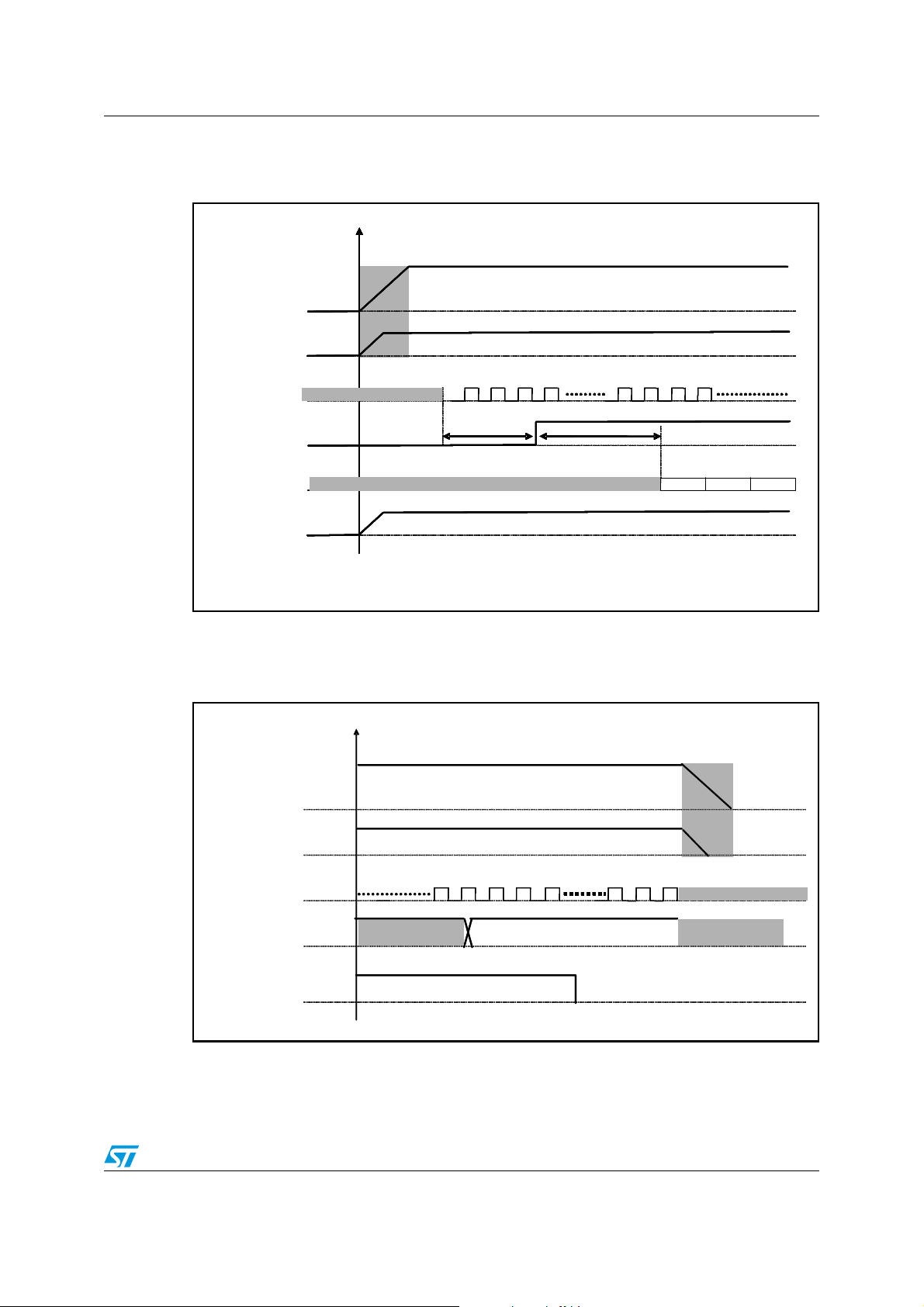
3.6 Power on/off sequence
Figure 4. Power-on sequence
VCC
VCC
VCC
VCC
VCC
VDD_Dig
VDD_Dig
VDD_Dig
VDD_Dig
VDD_Dig
XTI
XTI
XTI
XTI
XTI
Reset
Reset
Reset
Reset
Reset
2
2
2
2
2
C
C
C
C
C
I
I
I
I
I
PWDN
PWDN
PWDN
PWDN
PWDN
Note: no specific VCC and
VDD_DIG turn
is required
Don’t care
Don’t care
Don’t care
Don’t care
Don’t care
Don’t care
Don’t care
−
on sequence
TR
TR
TR
TR
TR
Don’t care
Don’t care
Don’t care
Don’t care
Don’t care
TC
TC
TC
TC
TC
CMD0 CMD1 CMD2
CMD0 CMD1 CMD2
CMD0 CMD1 CMD2
CMD0 CMD1 CMD2
CMD0 CMD1 CMD2
TR = minimum time between XTI master clock stable and Reset removal: 1 ms
TC = minimum time between Reset removal and I
Note: The definition of a stable clock is when f
Section : Serial data interface on page 28 gives information on setting up the I
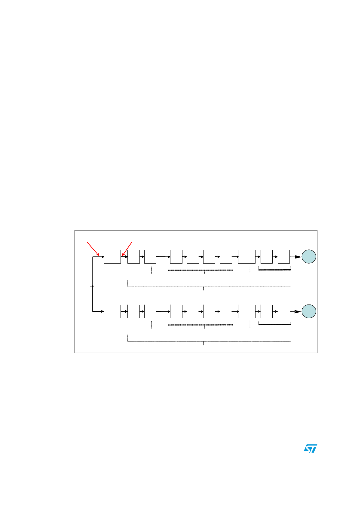
Figure 5. Power-off sequence for pop-free turn-off
VCC
VCC
VDD_Dig
VDD_Dig
XTI
XTI
Soft Mute
Soft Mute
Reg. 0x07
Reg. 0x07
Data 0xFE
Data 0xFE
Soft EAPD
Soft EAPD
Reg. 0x05
Reg. 0x05
Bit 7 = 0
Bit 7 = 0
Don’t care
Don’t care
2
C program, sequence start: 1ms
- f
max
< 1 MHz.
min
FE
FE
2
S interface.
Note: no specific VCC and
VDD_DIG turn
is required
Don’t care
Don’t care
Don’t care
Don’t care
−
off sequence
Don’t care
Don’t care
Don’t care
Don’t care
Doc ID 16861 Rev 4 17/89
Processing data paths STA369BWS
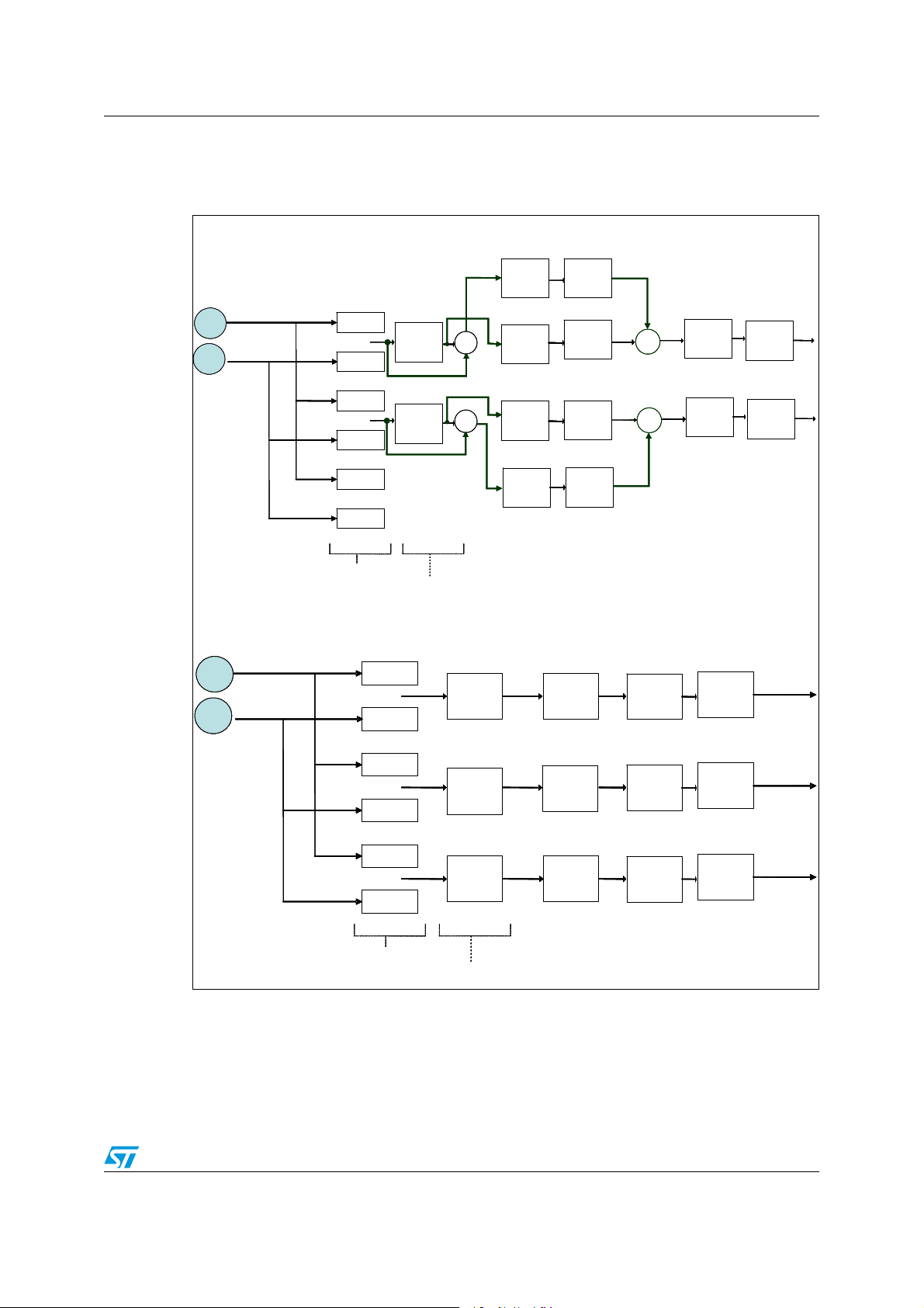
4 Processing data paths
Figure 6 and Figure 7 below show the data processing paths inside STA369BWS. The
whole processing chain is composed of two consecutive sections. In the first one,
dual-channel processing is implemented and in the second section each channel is fed into
the post-mixing block either to generate a third channel (typically used in 2.1 output
configuration and with crossover filters enabled) or to have the channels processed by the
dual-band DRC block (2.0 output configuration with crossover filters used to define the
cut-off frequency of the two bands).
The first section, Figure 6, begins with a 2x oversampling FIR filter providing 2 * f
audio
S
processing. Then a selectable high-pass filter removes the DC level (enabled if HPB = 0).
The left and right channel processing paths can include up to 8 filters, depending on the
selected configuration (bits BQL, BQ5, BQ6, BQ7 and XO[3:0]). By default, four user
programmable, independent filters per channel are enabled, plus the preconfigured
de-emphasis, bass and treble controls (BQL = 0, BQ5 = 0, BQ6 = 0, BQ7 = 0).
If the coefficient sets for the two channels are linked (BQL = 1) it is possible to use the
de-emphasis, bass and treble filters in a user defined configuration (provided the relevant
BQx bits are set). In this case both channels use the same processing coefficients and can
have up to seven filters each. If BQL = 0 the BQx bits are ignored and the fifth, sixth and
seventh filters are configured as de-emphasis, bass and treble controls, respectively.
Figure 6. Left and right processing, section 1
Sampling
Sampling
Sampling
Sampling
frequency=Fs
frequency=Fs
frequency=Fs
frequency=Fs
From
From
From
From
I2S input
I2S input
I2S input
I2S input
interface
interface
interface
interface
sampling
sampling
sampling
sampling
x2
x2
FIR
FIR
x2
x2
over
over
FIR
FIR
over
over
x2
x2
FIR
FIR
x2
x2
over
over
FIR
FIR
over
over
Sampling
Sampling
Sampling
Sampling
frequency=2xFs
frequency=2xFs
frequency=2xFs
frequency=2xFs
Hi-Pass
Hi-Pass
Hi-Pass
Hi-Pass
Hi-Pass
Hi-Pass
PreScale
PreScale
PreScale
PreScale
If HPB=0
If HPB=0
Hi-Pass
Hi-Pass
Hi-Pass
Hi-Pass
PreScale
PreScale
PreScale
PreScale
Filter
Filter
Filter
Filter
Filter
Filter
Filter
Filter
Filter
Filter
Biquad#1Biquad#2Biquad#3Biquad
Biquad#1Biquad#2Biquad#3Biquad
Biquad#1Biquad#2Biquad#3Biquad
Biquad#1Biquad#2Biquad#3Biquad
User Defined Filters
User Defined Filters
If DSPB=0 and C1EQBP=0
If DSPB=0 and C1EQBP=0
Biquad#1Biquad#2Biquad#3Biquad
Biquad#1Biquad#2Biquad#3Biquad
Biquad#1Biquad#2Biquad#3Biquad
Biquad#1Biquad#2Biquad#3Biquad
#4
#4
#4
#4
#4
#4
#4
#4
If BQ5=1
If BQ5=1
and BQL=1
and BQL=1
Biquad
Biquad
#5
#5
De-Emph.
De-Emph.
If DEMP=0
If DEMP=0
If BQ5=1
If BQ5=1
and BQL=1
and BQL=1
Biquad
Biquad
#5
#5
De-Emph.
De-Emph.
IF BQ7=1
IF BQ7=1
If BQ6=1
If BQ6=1
and BQL=1
and BQL=1
and BQL=1
and BQL=1
If C1TCB=0
If C1TCB=0
BTC: Bass Boost/Cut
BTC: Bass Boost/Cut
TTC: Treble Boost/Cut
TTC: Treble Boost/Cut
If BQ6=1
If BQ6=1
and BQL=1
and BQL=1
Biquad
Biquad
Biquad
Biquad
#6
#6
Bass Treble
Bass Treble
IF BQ7=1
IF BQ7=1
and BQL=1
and BQL=1
Biquad
Biquad
Biquad
Biquad
#6
#6
Bass Treble
Bass Treble
#7
#7
#7
#7
L
L
L
L
L
R
L
R
If HPB=0
If HPB=0
User Defined Filters
User Defined Filters
If DSPB=0 and C2EQBP=0
If DSPB=0 and C2EQBP=0
Moreover, the common 8th filter can be available on both channels provided the predefined
crossover frequencies are not used, XO[3:0] = 0, and the dual-band DRC is not used.
In the second section, Figure 7, mixing and crossover filters are available. If B
enabled they are fully user-programmable and allow the generation of a third channel
(2.1 outputs). Alternatively, in mode B
2
DRC, these blocks are used to split the sub-band and
define the cut-off frequencies of the two bands. A prescaler and a final postscaler allow full
control over the signal dynamics before and after the filtering stages. A mixer function is also
available.
18/89 Doc ID 16861 Rev 4
If DEMP=0
If DEMP=0
If C2TCB=0
If C2TCB=0
BTC: Bass Boost/Cut
BTC: Bass Boost/Cut
TTC: Treble Boost/Cut
TTC: Treble Boost/Cut
2
DRC is not
STA369BWS Processing data paths
In all the available configurations high-pass filtering with a 2-Hz cut-off frequency is applied
before the postscale block. This filter cannot be disabled.
Figure 7. Left and right processing, section 2
Dual-band DRC enabled
CH3
CH3
Volume
Volume
C1Mx1
C1Mx1=
C1Mx1
C1Mx1=
0x7fffff
L
L
L
L
R
R
R
R
0x7fffff
C1Mx2
C1Mx2=
C1Mx2
C1Mx2=
0x00000
0x00000
C2Mx1
C2Mx1=
C2Mx1
C2Mx1=
0x000000
0x000000
C2Mx2
C2Mx2=
C2Mx2
C2Mx2=
0x7fffff
0x7fffff
C3Mx1
C3Mx1=
C3Mx1
C3Mx1=
0x40000
0x40000
C3Mx2
C3Mx2=
C3Mx2
C3Mx2=
0x400000
0x400000
Hi-Pass XO
Hi-Pass XO
B2DRC
B2DRC
Filter
+
+
+
+
+
+
+
+
+
+
+
+
Filter
Hi-pass
Hi-pass
filter
filter
Hi-Pass XO
Hi-Pass XO
B2DRC
B2DRC
Filter
Filter
Hi-pass
Hi-pass
filter
filter
-
-++
+
-
-++
+
CH1
CH1
Volume
Volume
CH2
CH2
Volume
Volume
CH3
CH3
Volume
Volume
DRC2
DRC2
DRC1
DRC1
Limiter
Limiter
DRC1
DRC1
DRC2
DRC2
Vol
Vol
And
And
+
+
+
+
Post scale
Post scale
DC cut
DC cut
filter
filter
Post scale
Post scale
DC cut
DC cut
filter
filter
Post scale
Post scale
Post scale
Post scale
Post scale
Post scale
Post scale
Post scale
User-Defined Mix Coefficients
User-Defined Mix Coefficients
User-Defined Mix Coefficients
User-Defined Mix Coefficients
Dual-band DRC disabled
L
L
L
L
R
R
R
R
User-Defined Mix Coefficie nts
User-Defined Mix Coefficie nts
User-Defined Mix Coefficie nts
User-Defined Mix Coefficie nts
Crossover Frequency determined by XO Setting
Crossover Frequency determined by XO Setting
User Defined If XO =0000
User Defined If XO =0000
User Defined If XO =0000
User Defined If XO =0000
C1Mx1
C1Mx1
C1Mx1
C1Mx1
+
+
+
+
C1Mx2
C1Mx2
C1Mx2
C1Mx2
C2Mx1
C2Mx1
C2Mx1
C2Mx1
+
+
+
+
C2Mx2
C2Mx2
C2Mx2
C2Mx2
C3Mx1
C3Mx1
C3Mx1
C3Mx1
+
+
+
+
C3Mx2
C3Mx2
C3Mx2
C3Mx2
Channel ½
Channel ½
Hi-Pass XO
Hi-Pass XO
#8
Biquad #5
Biquad #5
Filter
Filter
--------------
--------------
Hi-pass XO
Hi-pass XO
filter
filter
Channel ½
Channel ½
Hi-Pass XO
Hi-Pass XO
#8
Biquad #5
Biquad #5
Filter
Filter
--------------
--------------
Hi-pass XO
Hi-pass XO
filter
filter
Channel 3
Channel 3
Lo-Pass XO
Lo-Pass XO
Biquad
Biquad
Filter
Filter
--------------
--------------
Low-pass XO
Low-pass XO
filter
filter
Crossover Frequency determined by XO Setting
Crossover Frequency determined by XO Setting
User Defined If XO=0000
User Defined If XO=0000
User Defined If XO=0000
User Defined If XO=0000
Vol
Vol
Vol
Vol
And
And
And
And
Limiter
Limiter
Limiter
Limiter
Vol
Vol
Vol
Vol
Vol
Vol
Vol
Vol
And
And
And
And
And
And
And
And
Limiter
Limiter
Limiter
Limiter
Limiter
Limiter
Limiter
Limiter
Vol
Vol
Vol
Vol
And
And
And
And
Limiter
Limiter
Limiter
Limiter
B2DRC Enabled
B2DRC Enabled
DC cutt
DC cutt
Post scale
Post scale
filter
filter
DC cutt
DC cutt
Post scale
Post scale
filter
filter
DC cutt
DC cutt
Post scale
Post scale
filter
filter
Post scale
Post scale
Post scale
Post scale
Post scale
Post scale
Post scale
Post scale
Post scale
Post scale
Post scale
Post scale
B2DRC Disabled
B2DRC Disabled
Doc ID 16861 Rev 4 19/89

I2C bus specification STA369BWS
5 I2C bus specification
The STA369BWS supports the I2C protocol via the input ports SCL and SDA_IN (master to
slave) and the output port SDA_OUT (slave to master). This protocol defines any device that
sends data on to the bus as a transmitter and any device that reads the data as a receiver.
The device that controls the data transfer is known as the master and the other as the slave.
The master always starts the transfer and provides the serial clock for synchronization. The
STA369BWS is always a slave device in all of its communications. It supports up to 400 kb/s
(fast-mode bit rate).
For correct operation of the I
has a frequency at least 10 times higher than the frequency of the applied SCL clock.
5.1 Communication protocol
5.1.1 Data transition or change
Data changes on the SDA line must only occur when the clock SCL is low. A SDA transition
while the clock is high is used to identify a START or STOP condition.
2
C interface ensure that the master clock generated by the PLL
5.1.2 Start condition
START is identified by a high to low transition of the data bus, SDA, while the clock, SCL, is
stable in the high state. A START condition must precede any command for data transfer.
5.1.3 Stop condition
STOP is identified by low to high transition of SDA while SCL is stable in the high state. A
STOP condition terminates communication between STA369BWS and the bus master.
5.1.4 Data input
During the data input the STA369BWS samples the SDA signal on the rising edge of SCL.
For correct device operation the SDA signal must be stable during the rising edge of the
clock and the data can change only when the SCL line is low.
5.2 Device addressing
To start communication between the master and the STA369BWS, the master must initiate
with a start condition. Following this, the master sends onto the SDA line 8-bits (MSB first)
corresponding to the device select address and read or write mode bit.
The seven most significant bits are the device address identifiers, corresponding to the I
bus definition. In the STA369BWS the I
the SA pin configuration, 0x38 when SA = 0, and 0x3A when SA = 1.
2
2
C interface has two device addresses depending on
C
The eighth bit (LSB) identifies a read or write operation (R/W); this is set to 1 for read and to
0 for write. After a START condition the STA369BWS identifies the device address on the
SDA bus and if a match is found, acknowledges the identification during the 9th bit time
frame. The byte following the device identification is the address of a device register.
20/89 Doc ID 16861 Rev 4
STA369BWS I2C bus specification
5.3 Write operation
Following the START condition the master sends a device select code with the RW bit set
to 0. The STA369BWS acknowledges this and then waits for the byte of internal address.
After receiving the internal byte address the STA369BWS again responds with an
acknowledgement.
5.3.1 Byte write
In the byte write mode the master sends one data byte, this is acknowledged by the
STA369BWS. The master then terminates the transfer by generating a STOP condition.
5.3.2 Multi-byte write
The multi-byte write modes can start from any internal address. The master generating a
STOP condition terminates the transfer.
Figure 8. Write mode sequence
BYTE
BYTE
WRITE
WRITE
MULTIBYTE
MULTIBYTE
WRITE
WRITE
START
START
START
START
DEV-ADDR
DEV-ADDR
DEV-ADDR
DEV-ADDR
ACK
ACK
SUB-ADDR
SUB-ADDR
RW
RW
ACK
ACK
SUB-ADDR
SUB-ADDR
RW
RW
ACK
ACK
ACK
ACK
DATA IN
DATA IN
DATA IN
DATA IN
ACK
ACK
ACK
ACK
STOP
STOP
DATA IN
DATA IN
ACK
ACK
STOP
STOP
5.4 Read operation
5.4.1 Current address byte read
Following the START condition the master sends a device select code with the RW bit set
to 1. The STA369BWS acknowledges this and then responds by sending one byte of data.
The master then terminates the transfer by generating a STOP condition.
5.4.2 Current address multi-byte read
The multi-byte read modes can start from any internal address. Sequential data bytes are
read from sequential addresses within the STA369BWS. The master acknowledges each
data byte read and then generates a STOP condition terminating the transfer.
5.4.3 Random address byte read
Following the START condition the master sends a device select code with the RW bit set
to 0. The STA369BWS acknowledges this and then the master writes the internal address
byte. After receiving, the internal byte address the STA369BWS again responds with an
acknowledgement. The master then initiates another START condition and sends the device
select code with the RW bit set to 1. The STA369BWS acknowledges this and then
responds by sending one byte of data. The master then terminates the transfer by
generating a STOP condition.
Doc ID 16861 Rev 4 21/89
I2C bus specification STA369BWS
5.4.4 Random address multi-byte read
The multi-byte read modes could start from any internal address. Sequential data bytes are
read from sequential addresses within the STA369BWS. The master acknowledges each
data byte read and then generates a STOP condition terminating the transfer.
Figure 9. Read mode sequence
CURRENT
CURRENT
ADDRESS
ADDRESS
READ
READ
RANDOM
RANDOM
ADDRESS
ADDRESS
READ
READ
SEQUENTIAL
SEQUENTIAL
CURRENT
CURRENT
READ
READ
SEQUENTIAL
SEQUENTIAL
RANDOM
RANDOM
READ
READ
START
START
START
START
START
START
START
START
DEV-ADDR
DEV-ADDR
DEV-ADDR
DEV-ADDR
DEV-ADDR
DEV-ADDR
DEV-ADDR
DEV-ADDR
RW=
RW=
HIGH
HIGH
ACK
ACK
RW
RW
ACK
ACK
RW
RW
ACK
ACK
ACK
ACK
RW
RW
DATA
DATA
SUB-ADDR
SUB-ADDR
DATA
DATA
SUB-ADDR
SUB-ADDR
NO ACK
NO ACK
STOP
STOP
ACK
ACK
ACK
ACK
ACK
ACK
DEV-ADDR
DEV-ADDR
START RW
START RW
DATA
DATA
DEV-ADDR
DEV-ADDR
START RW
START RW
ACK
ACK
ACK
ACK
ACK
ACK
DATA
DATA
DATA
DATA
DATA
DATA
NO ACK
NO ACK
NO ACK
NO ACK
ACK
ACK
STOP
STOP
STOP
STOP
DATA
DATA
ACK NO ACK
ACK NO ACK
DATA
DATA
STOP
STOP
22/89 Doc ID 16861 Rev 4

STA369BWS Register description
6 Register description
Note: Addresses exceeding the maximum address number must not be written.
Table 8. Register summary
Addr Name D7 D6 D5 D4 D3 D2 D1 D0
0x00 CONFA
0x01 CONFB
0x02 CONFC
0x03 CONFD
0x04 CONFE
0x05 CONFF
0x06 MUTELOC
0x07 MVOL
0x08 C1VOL
0x09 C2VOL
0x0A C3VOL
0x0B AUTO1
0x0C AUTO2
0x0D AUTO3
0x0E C1CFG
0x0F C2CFG
0x10 C3CFG
0x11 TONE
0x12 L1AR
0x13 L1ATRT
0x14 L2AR
0x15 L2ATRT
0x16 CFADDR
0x17 B1CF1
0x18 B1CF2
0x19 B1CF3
0x1A B2CF1
0x1B B2CF2
0x1C B2CF3
0x1D A1CF1
0x1E A1CF2
FDRB TWAB TWRB IR1 IR0 MCS2 MCS1 MCS0
C2IM C1IM DSCKE SAIFB SAI3 SAI2 SAI1 SAI0
OCRB Reserved CSZ3 CSZ2 CSZ1 CSZ0 OM1 OM0
SME ZDE DRC BQL PSL DSPB DEMP HPB
SVE ZCE DCCV PWMS AME NSBW MPC MPCV
EAPD PWDN ECLE LDTE BCLE IDE OCFG1 OCFG0
LOC1 LOC0 Reserved Reserved C3M C2M C1M Reserved
MVOL[7:0]
C1VOL[7:0]
C2VOL[7:0]
C3VOL[7:0]
Reserved Reserved AMGC[1:0] Reserved Reserved Reserved Reserved
XO3 XO2 XO1 XO0 AMAM2 AMAM1 AMAM0 AMAME
Reserved
C1OM1 C1OM0 C1LS1 C1LS0 C1BO C1VBP C1EQBP C1TCB
C2OM1 C2OM0 C2LS1 C2LS0 C2BO C2VBP C2EQBP C2TCB
C3OM1 C3OM0 C3LS1 C3LS0 C3BO C3VBP Reserved Reserved
TTC3 TTC2 TTC1 TTC0 BTC3 BTC2 BTC1 BTC0
L1A3 L1A2 L1A1 L1A0 L1R3 L1R2 L1R1 L1R0
L1AT3 L1AT2 L1AT1 L1AT0 L1RT3 L1RT2 L1RT1 L1RT0
L2A3 L2A2 L2A1 L2A0 L2R3 L2R2 L2R1 L2R0
L2AT3 L2AT2 L2AT1 L2AT0 L2RT3 L2RT2 L2RT1 L2RT0
Reserved Reserved CFA[5:0]
C1B[23:16]
C1B[15:8]
C1B[7:0]
C2B[23:16]
C2B[15:8]
C2B[7:0]
C3B[23:16]
C3B[15:8]
Doc ID 16861 Rev 4 23/89

Register description STA369BWS
Table 8. Register summary (continued)
Addr Name D7 D6 D5 D4 D3 D2 D1 D0
0x1F A1CF3
0x20 A2CF1
0x21 A2CF2
0x22 A2CF3
0x23 B0CF1
0x24 B0CF2
0x25 B0CF3
0x26 CFUD
0x27 MPCC1
0x28 MPCC2
0x29 DCC1
0x2A DCC2
0x2B FDRC1
0x2C FDRC2
0x2D STATUS
0x2E Reserved
0x2F Reserved
0x30 Reserved
0x31 EQCFG
0x32 EATH1
0x33 ERTH1
0x34 EATH2
0x35 ERTH2
0x36 CONFX
0x37 SVCA
0x38 SVCB
0x39 RMS0A
0x3A RMS0B
0x3B RMS0C
0x3C RMS1A
0x3D RMS1B
0x3E RMS1C
0x3F EVOLRES
0x40 Reserved
0x41 Reserved
C3B[7:0]
C4B[23:16]
C4B[15:8]
C4B[7:0]
C5B[23:16]
C5B[15:8]
C5B[7:0]
Reserved RA R1 WA W1
MPCC[15:8]
MPCC[7:0]
DCC[15:8]
DCC[7:0]
FDRC[15:8]
FDRC[7:0]
PLLUL FAULT UVFAULT Reserved OCFAULT OCWARN TFAULT TWARN
Reserved
Reserved
Reserved
XOB Reserved Reserved AMGC[3:2] Reserved SEL[1:0]
EATHEN1 EATH1[6:0]
ERTHEN1 ERTH1[6:0]
EATHEN2 EATH2[6:0]
ERTHEN2 ERTH2[6:0]
MDRC[1:0] PS48DB XAR1 XAR2 BQ5 BQ6 BQ7
Reserved Reserved SVUPE SVUP[4:0]
Reserved Reserved SVDWE SVDW[4:0]
R_C0[23:16]
R_C0[15:8]
R_C0[7:0]
R_C1[23:16]
R_C1[15:8]
R_C1[7:0]
VRESEN VRESTG C3VR[1:0] C2VR[1:0] C1VR[1:0]
Reserved
Reserved
24/89 Doc ID 16861 Rev 4

STA369BWS Register description
Table 8. Register summary (continued)
Addr Name D7 D6 D5 D4 D3 D2 D1 D0
0x42 Reserved
0x43 Reserved
0x44 Reserved
0x45 Reserved
0x46 SHOK
0x47 Reserved
0x48 NSHAPE
0x49 CXTB4B1
0x4A CXTB7B5
0x4B MISC1
0x4C MISC2
0x4D BPTH
0x4E BADPWM
0x4F BPTIM
0x50 Reserved
0x51 Reserved
0x52 Reserved
0x53 Reserved
0x54 Reserved
0x55 Reserved
0x56 Reserved
0x60 BQCHKE0
0x61 BQCHKE1
0x62 BQCHKE2
0x63 XCCHKE0
0x64 XCCHKE1
0x65 XCCHKE2
0x66 BQCHKR0
0x67 BQCHKR1
0x68 BQCHKR2
0x69 XCCHKR0
0x6A XCCHKR1
0x6B XCCHKR2
0x6C CHKCTRL
Reserved
Reserved
Reserved
Reserved
GND1A GND1B GND2A GND2B VCC1A VCC1B VCC2A VCC2B
Reserved
NSHXEN NSHB7EN NSHB6EN NSHB5EN NSHB4EN NSHB3EN NSHB2EN NSHB1EN
CXTB4[1:0] CXTB3[1:0] CXTB2[1:0] CXTB1[1:0]
Reserved Reserved CXTB7[1:0] CXTB6[1:0] CXTB5[1:0]
RPDNEN NSHHPEN BRIDGOFF F3XEN[1:0] CPWMEN Reserved BOOST
LPDP LPD LPDE PNDLSL[2:0] Reserved SHEN
BPTH[5:0] Reserved GDRC
BP4B BP4A BP3B BP3A BP2B BP2A BP1B BP1A
BPTIM[7:0]
Reserved
Reserved
Reserved
Reserved
Reserved
Reserved
Reserved
BQCHKE[7:0]
BQCHKE[15:8]
BQCHKE[23:16]
XCCHKE[7:0]
XCCHKE[15:8]
XCCHKE[23:16]
BQCHKR[7:0]
BQCHKR[15:8]
BQCHKR[23:16]
XCCHKR[7:0]
XCCHKR[15:8]
XCCHKR[23:16]
XCAUTO XCRES XCCMP XCGO BCAUTO BCRES BCCMP BCGO
Doc ID 16861 Rev 4 25/89
Register description STA369BWS
6.1 Configuration registers (addr 0x00 to 0x05)
6.1.1 Configuration register A (addr 0x00)
D7 D6 D5 D4 D3 D2 D1 D0
FDRB TWAB TWRB IR1 IR0 MCS2 MCS1 MCS0
01100011
Master clock select
Table 9. Master clock select
Bit R/W RST Name Description
0R/W1 MCS0
1R/W1 MCS1
Selects the ratio between the input I
frequency and the input clock.
2
S sample
2R/W0 MCS2
The STA369BWS supports sample rates of 32 kHz, 44.1 kHz, 48 kHz, 88.2 kHz, 96 kHz,
176.4 kHz, and 192 kHz. Therefore the internal clock is:
z 32.768 MHz for 32 kHz
z 45.1584 MHz for 44.1 kHz, 88.2 kHz, and 176.4 kHz
z 49.152 MHz for 48 kHz, 96 kHz, and 192 kHz
The external clock frequency provided to the XTI pin must be a multiple of the input sample
frequency (f
).
s
The relationship between the input clock and the input sample rate is determined by both
the MCSx and the IR (input rate) register bits. The MCSx bits determine the PLL factor
generating the internal clock and the IR bit determines the oversampling ratio used
internally.
Table 10. Input sampling rates
Input sample rate
fs (kHz)
IR MCS[2:0]
101 100 011 010 001 000
32, 44.1, 48 00 576 * fs 128 * fs 256 * fs 384 * fs 512 * fs 768 * fs
88.2, 96 01 NA 64 * fs 128 * fs 192 * fs 256 * fs 384 * fs
176.4, 192 1X NA 32 * fs 64 * fs 96 * fs 128 * fs 192 * fs
Interpolation ratio select
Table 11. Internal interpolation ratio
Bit R/W RST Name Description
4:3 R/W 00 IR [1:0]
26/89 Doc ID 16861 Rev 4
Selects internal interpolation ratio based on input I
sample frequency
2
S

STA369BWS Register description
The STA369BWS has variable interpolation (oversampling) settings such that internal
processing and FFX output rates remain consistent. The first processing block interpolates
by either 2-times or 1-time (pass-through) or provides a 2-times downsample. The
oversampling ratio of this interpolation is determined by the IR bits.
Table 12. IR bit settings as a function of input sample rate
Input sample rate fs (kHz) IR 1st stage interpolation ratio
32 00 2-times oversampling
44.1 00 2-times oversampling
48 00 2-times oversampling
88.2 01 Pass-through
96 01 Pass-through
176.4 10 2-times downsampling
192 10 2-times downsampling
Thermal warning recovery bypass
Table 13. Thermal warning recovery bypass
Bit R/W RST Name Description
5R/W1 TWRB
0: thermal warning recovery enabled
1: thermal warning recovery disabled
This bit sets the behavior of the IC after a thermal warning disappears. If TWRB is enabled
the device automatically restores the normal gain and output limiting is no longer active. If it
is disabled the device keeps the output limit active until a reset is asserted or until TWRB set
to 0. This bit works in conjunction with TWAB
Thermal warning adjustment bypass
Table 14. Thermal warning adjustment bypass
Bit R/W RST Name Description
6R/W1 TWAB
Bit TWAB enables automatic output limiting when a power stage thermal warning condition
persists for longer than 400ms. When the feature is active (TWAB = 0) the desired output
limiting, set through bit TWOCL (-3 dB by default) at address 0x37 in the RAM coefficients
bank, is applied. The way the limiting acts after the warning condition disappears is
controlled by bit TWRB.
0: thermal warning adjustment enabled
1: thermal warning adjustment disabled
Doc ID 16861 Rev 4 27/89

Register description STA369BWS
Fault detect recovery bypass
Table 15. Fault detect recovery bypass
Bit R/W RST Name Description
7 R/W 0 FDRB
0: fault detect recovery enabled
1: fault detect recovery disabled
The on-chip power block provides feedback to the digital controller which is used to indicate
a fault condition (either overcurrent or thermal). When fault is asserted the power control
block attempts a recovery from the fault by asserting the 3-state output, holding it for period
of time in the range of 0.1 ms to 1 second, as defined by the fault-detect recovery constant
register (FDRC registers 0x2B-0x2C), then toggling it back to normal condition. This
sequence is repeated as long as the fault indication exists. This feature is enabled by default
but can be bypassed by setting the FDRB control bit to 1. The fault condition is also
asserted by a low-state pulse of the normally high INT_LINE output pin.
6.1.2 Configuration register B (addr 0x01)
D7 D6 D5 D4 D3 D2 D1 D0
C2IM C1IM DSCKE SAIFB SAI3 SAI2 SAI1 SAI0
10000000
Serial audio input interface format
Table 16. Serial audio input interface
Bit R/W RST Name Description
0R/W0 SAI0
1R/W0 SAI1
2R/W0 SAI2
3R/W0 SAI3
Determines the interface format of the input serial
digital audio interface.
Serial data interface
The STA369BWS audio serial input interfaces with standard digital audio components and
accepts a number of serial data formats. STA369BWS always acts as slave when receiving
audio input from standard digital audio components. Serial data for two channels is provided
using three inputs: left/right clock LRCKI, serial clock BICKI, and serial data SDI.
Bits SAI and bit SAIFB are used to specify the serial data format. The default serial data
format is I
2
S, MSB first. Available formats are shown in the tables and figure that follow.
Serial data first bit
Table 17. Serial data first bit
SAIFB Format
0 MSB-first
1 LSB-first
28/89 Doc ID 16861 Rev 4

STA369BWS Register description
Table 18. Support serial audio input formats for MSB-first (SAIFB = 0)
BICKI SAI [3:0] SAIFB Interface format
32 * fs
0000 0 I
0001 0 Left/right-justified 16-bit data
0000 0 I
0001 0 Left-justified 16 to 24-bit data
0010 0 Right-justified 24-bit data
48 * fs
0110 0 Right-justified 20-bit data
1010 0 Right-justified 18-bit data
1110 0 Right-justified 16-bit data
0000 0 I2S 16 to 24-bit data
0001 0 Left-justified 16 to 24-bit data
0010 0 Right-justified 24-bit data
64 * fs
0110 0 Right-justified 20-bit data
1010 0 Right-justified 18-bit data
1110 0 Right-justified 16-bit data
2
S 15-bit data
2
S 16 to 23-bit data
Table 19. Supported serial audio input formats for LSB-first (SAIFB = 1)
BICKI SAI [3:0] SAIFB Interface Format
1100 1 I
2
S 15-bit data
32 * fs
1110 1 Left/right-justified 16-bit data
0100 1 I
0100 1 I
1000 1 I
1100 1 LSB first I
2
S 23-bit data
2
S 20-bit data
2
S 18-bit data
2
S 16-bit data
0001 1 Left-justified 24-bit data
0101 1 Left-justified 20-bit data
48 * fs
1001 1 Left-justified 18-bit data
1101 1 Left-justified 16-bit data
0010 1 Right-justified 24-bit data
0110 1 Right-justified 20-bit data
1010 1 Right-justified 18-bit data
1110 1 Right-justified 16-bit data
Doc ID 16861 Rev 4 29/89

Register description STA369BWS
Table 19. Supported serial audio input formats for LSB-first (SAIFB = 1) (continued)
BICKI SAI [3:0] SAIFB Interface Format
0000 1 I2S 24-bit data
0100 1 I
1000 1 I
1100 1 LSB first I
0001 1 Left-justified 24-bit data
0101 1 Left-justified 20-bit data
64 * fs
1001 1 Left-justified 18-bit data
1101 1 Left-justified 16-bit data
0010 1 Right-justified 24-bit data
0110 1 Right-justified 20-bit data
1010 1 Right-justified 18-bit data
1110 1 Right-justified 16-bit data
2
S 20-bit data
2
S 18-bit data
2
S 16-bit data
To make the STA369BWS work properly, the serial audio interface LRCKI clock must be
synchronous to the PLL output clock. It means that:
N-4< = (frequency of PLL clock) / (frequency of LRCKI) = < N+4 cycles,
where N depends on the settings in Table 12 on page 27.
the PLL must be locked.
If these two conditions are not met, and IDE bit (register 0x05, bit 2) is set to 1, the
STA369BWS immediately mutes the I
2
S PCM data out (provided to the processing block)
and it freezes any active processing task.
Clock desyncronization can happen during STA369BWS operation because of source
switching or TV channel change. To avoid audio side effects, like click or pop noise, it is
strongly recommended to complete the following actions:
1. soft volume change
2
2. I
C read /write instructions
while the serial audio interface and the internal PLL are still synchronous.
Delay serial clock enable
Table 20. Delay serial clock enable
Bit R/W RST Name Description
0: no serial clock delay
5 R/W 0 DSCKE
1: serial clock delay by 1 core clock cycle to tolerate
anomalies in some I2S master devices
30/89 Doc ID 16861 Rev 4

STA369BWS Register description
Channel input mapping
Table 21. Channel input mapping
Bit R/W RST Name Description
2
6R/W0 C1IM
7R/W1 C2IM
0: processing channel 1 receives left I
1: processing channel 1 receives right I2S Input
0: processing channel 2 receives left I
1: processing channel 2 receives right I2S Input
S Input
2
S Input
Each channel received via I2S can be mapped to any internal processing channel via the
channel input mapping registers. This allows for flexibility in processing. The default settings
of these registers maps each I
2
S input channel to its corresponding processing channel.
6.1.3 Configuration register C (addr 0x02)
D7 D6 D5 D4 D3 D2 D1 D0
OCRB Reserved CSZ3 CSZ2 CSZ1 CSZ0 OM1 OM0
10010111
FFX power output mode
The FFX power output mode selects how the FFX output timing is configured.
Different power devices use different output modes.
Table 22. FFX power output mode
Bit R/W RST Name Description
0 R/W 1 OM0 Selects configuration of FFX output:
00: drop compensation
1R/W1 OM1
01: discrete output stage: tapered compensation
10: full-power mode
11: variable drop compensation (CSZx bits)
FFX compensating pulse size register
Table 23. FFX compensating pulse size bits
Bit R/W RST Name Description
2R/W1 CSZ0
3R/W1 CSZ1
4R/W1 CSZ2
5R/W0 CSZ3
When OM[1,0] = 11, this register determines the
size of the FFX compensating pulse from 0 clock
ticks to 15 clock periods.
Doc ID 16861 Rev 4 31/89

Register description STA369BWS
Table 24. Compensating pulse size
CSZ[3:0] Compensating pulse size
0000 0 ns (0 tick) compensating pulse size
0001 20 ns (1 tick) clock period compensating pulse size
……
1111 300 ns (15 tick) clock period compensating pulse size
Overcurrent warning adjustment bypass
Table 25. Overcurrent warning bypass
Bit R/W RST Name Description
7 R/W 1 OCRB
0: overcurrent warning adjustment enabled
1: overcurrent warning adjustment disabled
The OCRB is used to indicate how STA369BWS behaves when an overcurrent warning
condition occurs. If OCRB = 0 and the overcurrent condition happens, the power control
block forces an adjustment to the modulation limit (default is -3 dB) in an attempt to
eliminate the overcurrent warning condition. Once the overcurrent warning clipping
adjustment is applied, it remains in this state until reset is applied or OCRB is set to 1. The
level of adjustment can be changed via the TWOCL (thermal warning/overcurrent limit)
setting at address 0x37 of the user defined coefficient RAM (Section 6.7.7 on page 59). The
OCRB can be enabled while the output bridge is already on.
6.1.4 Configuration register D (addr 0x03)
D7 D6 D5 D4 D3 D2 D1 D0
SME ZDE DRC BQL PSL DSPB DEMP HPB
01000000
High-pass filter bypass
Table 26. High-pass filter bypass
Bit R/W RST Name Description
0 R/W 0 HPB 1: bypass internal AC coupling digital high-pass filter
The STA369BWS features an internal digital high-pass filter for the purpose of AC coupling.
The purpose of this filter is to prevent DC signals from passing through a FFX amplifier. DC
signals can cause speaker damage. When HPB = 0, this filter is enabled.
32/89 Doc ID 16861 Rev 4

STA369BWS Register description
De-emphasis
Table 27. De-emphasis
Bit R/W RST Name Description
1R/W0 DEMP
0: no de-emphasis
1: enable de-emphasis on all channels
DSP bypass
Table 28. DSP bypass
Bit R/W RST Name Description
2 R/W 0 DSPB
0: normal operation
1: bypass of biquad and bass/treble functions
Setting the DSPB bit bypasses the EQ function of the STA369BWS.
Postscale link
Table 29. Postscale link
Bit R/W RST Name Description
3R/W0 PSL
Postscale functionality can be used for power-supply error correction. For multi-channel
applications running off the same power-supply, the postscale values can be linked to the
value of channel 1 for ease of use and update the values faster.
0: each channel uses individual postscale value
1: each channel uses channel 1 postscale value
Biquad coefficient link
Table 30. Biquad coefficient link
Bit R/W RST Name Description
4R/W0 BQL
0: each channel uses coefficient values
1: each channel uses channel 1 coefficient values
For ease of use, all channels can use the biquad coefficients loaded into the Channel-1
coefficient RAM space by setting the BQL bit to 1. Therefore, any EQ updates only have to
be performed once.
Dynamic range compression/anti-clipping bit
Table 31. Dynamic range compression/anti-clipping bit
Bit R/W RST Name Description
5 R/W 0 DRC
Doc ID 16861 Rev 4 33/89
0: limiters act in anti-clipping mode
1: limiters act in dynamic range compression mode

Register description STA369BWS
Both limiters can be used in one of two ways, anti-clipping or dynamic range compression.
When used in anti-clipping mode the limiter threshold values are constant and dependent on
the limiter settings. In dynamic range compression mode the limiter threshold values vary
with the volume settings allowing a nighttime listening mode that provides a reduction in the
dynamic range regardless of the volume level.
Zero-detect mute enable
Table 32. Zero-detect mute enable
Bit R/W RST Name Description
6R/W1 ZDE
0: automatic zero-detect mute disabled
1: automatic zero-detect mute enabled
Setting the ZDE bit enables the zero-detect automatic mute. The zero-detect circuit looks at
the data for each processing channel at the output of the crossover (bass management)
filter. If any channel receives 2048 consecutive zero value samples (regardless of fs) then
that individual channel is muted if this function is enabled.
Submix mode enable
Table 33. Submix mode enable
Bit R/W RST Name Description
7R/W0 SME
0: submix into left/right disabled
1: submix into left/right enabled
6.1.5 Configuration register E (addr 0x04)
D7 D6 D5 D4 D3 D2 D1 D0
SVE ZCE DCCV PWMS AME NSBW MPC MPCV
11000010
Max power correction variable
Table 34. Max power correction variable
Bit R/W RST Name Description
0R/W0 MPCV
0: use standard MPC coefficient
1: use MPCC bits for MPC coefficient
Max power correction
Table 35. Max power correction
Bit R/W RST Name Description
0: function disabled
1R/W1 MPC
34/89 Doc ID 16861 Rev 4
1: enables power bridge correction for THD
reduction near maximum power output.

STA369BWS Register description
Setting the MPC bit turns on special processing that corrects the STA369BWS power device
at high power. This mode should lower the THD+N of a full FFX system at maximum power
output and slightly below. If enabled, MPC is operational in all output modes except tapered
(OM[1,0] = 01) and binary. When OCFG = 00, MPC has no effect on channels 3 and 4, the
line-out channels.
Noise-shaper bandwidth selection
Table 36. Noise-shaper bandwidth selection
Bit R/W RST Name Description
2 R/W 0 NSBW
1: third-order NS
0: fourth-order NS
AM mode enable
Table 37. AM mode enable
Bit R/W RST Name Description
3R/W0 AME
0: normal FFX operation.
1: AM reduction mode FFX operation
STA369BWS features a FFX processing mode that minimizes the amount of noise
generated in frequency range of AM radio. This mode is intended for use when FFX is
operating in a device with an AM tuner active. The SNR of the FFX processing is reduced to
approximately 83 dB in this mode, which is still greater than the SNR of AM radio.
PWM speed mode
Table 38. PWM speed mode
Bit R/W RST Name Description
4R/W0 PWMS
0: normal speed (384 kHz) all channels
1: odd speed (341.3 kHz) all channels
Distortion compensation variable enable
Table 39. Distortion compensation variable enable
Bit R/W RST Name Description
5 R/W 0 DCCV
Doc ID 16861 Rev 4 35/89
0: use preset DC coefficient
1: use DCC coefficient

Register description STA369BWS
Zero-crossing volume enable
Table 40. Zero-crossing volume enable
Bit R/W RST Name Description
1: volume adjustments only occur at digital zero-
6R/W1 ZCE
crossings
0: volume adjustments occur immediately
The ZCE bit enables zero-crossing volume adjustments. When volume is adjusted on digital
zero-crossings no clicks are audible.
Soft volume update enable
Table 41. Soft volume update enable
Bit R/W RST Name Description
1: volume adjustments ramp according to SVUP/SVDW
7 R/W 1 SVE
settings
0: volume adjustments occur immediately
6.1.6 Configuration register F (addr 0x05)
D7 D6 D5 D4 D3 D2 D1 D0
EAPD PWDN ECLE LDTE BCLE IDE OCFG1 OCFG0
01011100
Output configuration
Table 42. Output configuration
Bit R/W RST Name Description
0 R/W 0 OCFG0
1 R/W 0 OCFG1
Selects the output configuration
36/89 Doc ID 16861 Rev 4

STA369BWS Register description
Table 43. Output configuration engine selection
OCFG[1:0] Output configuration Config pin
2 channel (full-bridge) power, 2 channel data-out:
1A/1B → 1A/1B
00
01
10
11
2A/2B → 2A/2B
LineOut1 → 3A/3B
LineOut2 → 4A/4B
Line Out Configuration determined by LOC register
2 (half-bridge), 1(full-bridge) on-board power:
1A → 1A Binary 0 °
2A → 1B Binary 90°
3A/3B → 2A/2B Binary 45°
1A/B → 3A/B Binary 0°
2A/B → 4A/B Binary 90°
2 channel (full-bridge) power, 1 channel FFX:
1A/1B → 1A/1B
2A/2B → 2A/2B
3A/3B → 3A/3B
EAPDEXT and TWARNEXT Active
1 channel mono-parallel:
3A → 1A/1B w/ C3BO 45°
3B → 2A/2B w/ C3BO 45°
1A/1B → 3A/3B
2A/2B → 4A/4B
0
0
0
1
Note: To the left of the arrow is the processing channel. When using channel output mapping, any
of the three processing channel outputs can be used for any of the three inputs.
Figure 10. OCFG = 00 (default value)
OUT1A
OUT1A
Half
Half
Bridge
Bridge
Channel 1
LPF
LPF
LPF
LPF
Channel 1
Channel 2
Channel 2
LineOut1
LineOut1
LineOut2
LineOut2
Half
Half
Bridge
Bridge
Half
Half
Bridge
Bridge
Half
Half
Bridge
Bridge
OUT1B
OUT1B
OUT2A
OUT2A
OUT2B
OUT2B
OUT3A
OUT3A
OUT3B
OUT3B
OUT4A
OUT4A
OUT4B
OUT4B
Doc ID 16861 Rev 4 37/89

Register description STA369BWS
Figure 11. OCFG = 01
Half
Half
Bridge
Bridge
Half
Half
Bridge
Bridge
Half
Half
Bridge
Bridge
Half
Half
Bridge
Bridge
OUT1A
OUT1A
OUT1B
OUT1B
OUT2A
OUT2A
OUT2B
OUT2B
Channel 1
Channel 1
Channel 2
Channel 2
Channel 3
Channel 3
Figure 12. OCFG = 10
OUT1A
OUT1A
Half
Half
Bridge
Bridge
Channel 1
Half
Half
Bridge
Bridge
Half
Half
Bridge
Bridge
Half
Half
Bridge
Bridge
OUT1B
OUT1B
OUT2A
OUT2A
OUT2B
OUT2B
Channel 1
Channel 2
Channel 2
OUT3A
OUT3A
OUT3B
OUT3B
Power
EAPD
EAPD
Power
Device
Device
Channel 3
Channel 3
Figure 13. OCFG = 11
OUT1A
OUT1A
Half
Half
Bridge
Bridge
OUT1B
OUT2B
OUT2B
OUT3A
OUT3A
OUT3B
OUT3B
OUT4A
OUT4A
OUT4B
OUT4B
OUT1B
OUT2A
OUT2A
Channel 1
Channel 1
Channel 2
Channel 2
Channel 3
Channel 3
Half
Half
Bridge
Bridge
Half
Half
Bridge
Bridge
Half
Half
Bridge
Bridge
The STA369BWS can be configured to support different output configurations. For each
PWM output channel a PWM slot is defined. A PWM slot is always 1 / (8 * fs) seconds
length. The PWM slot define the maximum extension for PWM rise and fall edge, that is,
rising edge as far as the falling edge cannot range outside PWM slot boundaries.
38/89 Doc ID 16861 Rev 4

STA369BWS Register description
Figure 14. Output mapping scheme
FFX1A
FFX1A
FFX1A
FFX1A
FFX1A
FFX ™
FFX ™
FFX ™
FFX ™
FFX ™
FFX ™
modulator
modulator
modulator
modulator
modulator
modulator
FFX1A
FFX1 B
FFX1 B
FFX1 B
FFX1 B
FFX1 B
FFX1 B
FFX2 A
FFX2 A
FFX2 A
FFX2 A
FFX2 A
FFX2 A
FFX 2B
FFX 2B
FFX 2B
FFX 2B
FFX 2B
FFX 2B
FFX3 A
FFX3 A
FFX3 A
FFX3 A
FFX3 A
FFX3 A
FFX3B
FFX3B
FFX3B
FFX3B
FFX3B
FFX3B
FFX4 A
FFX4 A
FFX4 A
FFX4 A
FFX4 A
FFX4 A
FFX 4B
FFX 4B
FFX 4B
FFX 4B
FFX 4B
REMAP
REMAP
REMAP
REMAP
REMAP
REMAP
OUT1A
OUT1A
OUT1A
OUT1A
OUT1A
OUT1A
OUT1B
OUT1B
OUT1B
OUT1B
OUT1B
OUT1B
OUT2A
OUT2A
OUT2A
OUT2A
OUT2A
OUT2A
OUT2B
OUT2B
OUT2B
OUT2B
OUT2B
OUT2B
OUT3A
OUT3A
OUT3A
OUT3A
OUT3A
OUT3B
OUT3B
OUT3B
OUT3B
OUT3B
OUT4A
OUT4A
OUT4A
OUT4A
OUT4A
Power
Power
Power
Power
Power
Power
Bridge
Bridge
Bridge
Bridge
Bridge
Bridge
OUT1A
OUT1A
OUT1A
OUT1A
OUT1A
OUT1A
OUT1B
OUT1B
OUT1B
OUT1B
OUT1B
OUT1B
OUT2A
OUT2A
OUT2A
OUT2A
OUT2A
OUT2A
OUT2B
OUT2B
OUT2B
OUT2B
OUT2B
OUT2B
OUT4B
OUT4B
OUT4B
OUT4B
OUT4B
For each configuration the PWM signals from the digital driver are mapped in different ways
to the power stage:
Doc ID 16861 Rev 4 39/89

Register description STA369BWS
2.0 channels, two full-bridges (OCFG = 00)
Mapping:
z FFX1A -> OUT1A
z FFX1B -> OUT1B
z FFX2A -> OUT2A
z FFX2B -> OUT2B
z FFX3A -> OUT3A
z FFX3B -> OUT3B
z FFX4A -> OUT4A
z FFX4B -> OUT4B
Default modulation:
z FFX1A/1B configured as ternary
z FFX2A/2B configured as ternary
z FFX3A/3B configured as lineout ternary
z FFX4A/4B configured as lineout ternary
On channel 3 line out (LOC bits = 00) the same data as channel 1 processing is sent. On
channel 4 line out (LOC bits = 00) the same data as channel 2 processing is sent. In this
configuration, volume control or EQ have no effect on channels 3 and 4.
In this configuration the PWM slot phase is the following as shown in Figure 15.
Figure 15. 2.0 channels (OCFG = 00) PWM slots
OUT1A
OUT1A
OUT1B
OUT1B
OUT2A
OUT2A
OUT2B
OUT2B
OUT3A
OUT3A
OUT3B
OUT3B
OUT4A
OUT4A
OUT4B
OUT4B
40/89 Doc ID 16861 Rev 4

STA369BWS Register description
2.1 channels, two half-bridges + one full-bridge (OCFG = 01)
Mapping:
z FFX1A -> OUT1A
z FFX2A -> OUT1B
z FFX3A -> OUT2A
z FFX3B -> OUT2B
z FFX1A -> OUT3A
z FFX1B -> OUT3B
z FFX2A -> OUT4A
z FFX2B -> OUT4B
Modulation:
z FFX1A/1B configured as binary
z FFX2A/2B configured as binary
z FFX3A/3B configured as binary
z FFX4A/4B configured as binary
In this configuration, channel 3 has full control (volume, EQ, etc…). On OUT3/OUT4
channels the channel 1 and channel 2 PWM are replicated.
In this configuration the PWM slot phase is the following as shown in Figure 16.
Figure 16. 2.1 channels (OCFG = 01) PWM slots
OUT1A
OUT1A
OUT1A
OUT1A
OUT1A
OUT1A
OUT1B
OUT1B
OUT1B
OUT1B
OUT1B
OUT1B
OUT2A
OUT2A
OUT2A
OUT2A
OUT2A
OUT2A
OUT2B
OUT2B
OUT2B
OUT2B
OUT2B
OUT2B
OUT3A
OUT3A
OUT3A
OUT3A
OUT3A
OUT3A
OUT3B
OUT3B
OUT3B
OUT3B
OUT3B
OUT3B
OUT4A
OUT4A
OUT4A
OUT4A
OUT4A
OUT4B
OUT4B
OUT4B
OUT4B
OUT4B
Doc ID 16861 Rev 4 41/89

Register description STA369BWS
2.1 channels, two full-bridges + one external full-bridge (OCFG = 10)
Mapping:
z FFX1A -> OUT1A
z FFX1B -> OUT1B
z FFX2A -> OUT2A
z FFX2B -> OUT2B
z FFX3A -> OUT3A
z FFX3B -> OUT3B
z EAPD -> OUT4A
z TWARN -> OUT4B
Default modulation:
z FFX1A/1B configured as ternary
z FFX2A/2B configured as ternary
z FFX3A/3B configured as ternary
z FFX4A/4B is not used
In this configuration, channel 3 has full control (volume, EQ, etc…). On OUT4 channel the
external bridge control signals are muxed.
In this configuration the PWM slot phase is the following as shown in Figure 17.
Figure 17. 2.1 channels (OCFG = 10) PWM slots
OUT1A
OUT1A
OUT1A
OUT1A
OUT1B
OUT1B
OUT1B
OUT1B
OUT2A
OUT2A
OUT2A
OUT2A
OUT2B
OUT2B
OUT2B
OUT2B
OUT3A
OUT3A
OUT3A
OUT3A
OUT3B
OUT3B
OUT3B
OUT3B
42/89 Doc ID 16861 Rev 4

STA369BWS Register description
Invalid input detect mute enable
Table 44. Invalid input detect mute enable
Bit R/W RST Name Description
2R/W1 IDE
0: disables the automatic invalid input detect mute
1: enables the automatic invalid input detect mute
Setting the IDE bit enables this function, which looks at the input I2S data and automatically
mutes if the signals are perceived as invalid.
Binary output mode clock loss detection
Table 45. Binary output mode clock loss detection
Bit R/W RST Name Description
3R/W1 BCLE
0: binary output mode clock loss detection disabled
1: binary output mode clock loss detection enable
Detects loss of input MCLK in binary mode and will output 50% duty cycle.
LRCK double trigger protection
Table 46. LRCK double trigger protection
Bit R/W RST Name Description
4R/W1 LDTE
0: LRCLK double trigger protection disabled
1: LRCLK double trigger protection enabled
LDTE, when enabled, prevents double trigger of LRCLK on instable I2S input.
Auto EAPD on clock loss
Table 47. Auto EAPD on clock loss
Bit R/W RST Name Description
5R/W0 ECLE
0: auto EAPD on clock loss not enabled
1: auto EAPD on clock loss
When active, issues a power device power down signal (EAPD) on clock loss detection.
IC power down
Table 48. IC power down
Bit R/W RST Name Description
6R/W1 PWDN
Doc ID 16861 Rev 4 43/89
0: IC power down low-power condition
1: IC normal operation

Register description STA369BWS
The PWDN register is used to place the IC in a low-power state. When PWDN is written
as 0, the output begins a soft-mute. After the mute condition is reached, EAPD is asserted
to power down the power-stage, then the master clock to all internal hardware expect the
2
I
C block is gated. This places the IC in a very low power consumption state.
External amplifier power down
Table 49. External amplifier power down
Bit R/W RST Name Description
7R/W0 EAPD
0: external power stage power down active
1: normal operation
The EAPD register directly disables/enables the internal power circuitry.
When EAPD = 0, the internal power section is placed in a low-power state (disabled). This
register also controls the FFX4B / EAPD output pin when OCFG = 10.
6.2 Volume control registers (addr 0x06 - 0x0A)
The volume structure of the STA369BWS consists of individual volume registers for each
channel and a master volume register that provides an offset to each channels volume
setting. The individual channel volumes are adjustable in 0.5 dB steps from +48 dB
to -80 dB.
As an example if C3VOL = 0x00 or +48 dB and MVOL = 0x18 or -12 dB, then the total gain
for channel 3 = +36 dB.
The channel mutes provide a “soft mute” with the volume ramping down to mute in
4096 samples from the maximum volume setting at the internal processing rate
(approximately 96 kHz).
A “hard (instantaneous) mute” can be obtained by programming a value of 0xFF (255) in any
channel volume register. When volume offsets are provided via the master volume register
any channel whose total volume is less than -80 dB is muted.
All changes in volume take place at zero-crossings when ZCE = 1 (Configuration register E
(addr 0x04) on page 34) on a per channel basis as this creates the smoothest possible
volume transitions. When ZCE = 0, volume updates occur immediately.
44/89 Doc ID 16861 Rev 4

STA369BWS Register description
6.2.1 Mute/line output configuration register (addr 0x06)
D7 D6 D5 D4 D3 D2 D1 D0
LOC1 LOC0 Reserved Reserved C3M C2M C1M Reserved
00000000
Table 50. Line output configuration
LOC[1:0] Line output configuration
00 Line output fixed - no volume, no EQ
01 Line output variable - channel 3 volume effects line output, no EQ
10 Line output variable with EQ - channel 3 volume effects line output
Line output is only active when OCFG = 00. In this case LOC determines the line output
configuration. The source of the line output is always the channel 1 and 2 inputs.
6.2.2 Master volume register (addr 0x07)
D7 D6 D5 D4 D3 D2 D1 D0
MVOL7 MVOL6 MVOL5 MVOL4 MVOL3 MVOL2 MVOL1 MVOL0
11111111
Table 51. Master volume offset as a function of MVOL[7:0]
MVOL[7:0] Volume offset from channel value
00000000 (0x00) 0 dB
00000001 (0x01) -0.5 dB
00000010 (0x02) -1 dB
……
01001100 (0x4C) -38 dB
……
11111110 (0xFE) -127.5 dB
11111111 (0xFF) Default mute, not to be used during operation
6.2.3 Channel 1 volume (addr 0x08)
D7 D6 D5 D4 D3 D2 D1 D0
C1VOL7 C1VOL6 C1VOL5 C1VOL4 C1VOL3 C1VOL2 C1VOL1 C1VOL0
01100000
6.2.4 Channel 2 volume (addr 0x09)
D7 D6 D5 D4 D3 D2 D1 D0
C2VOL7 C2VOL6 C2VOL5 C2VOL4 C2VOL3 C2VOL2 C2VOL1 C2VOL0
01100000
Doc ID 16861 Rev 4 45/89

Register description STA369BWS
6.2.5 Channel 3 / line output volume (addr 0x0A)
D7 D6 D5 D4 D3 D2 D1 D0
C3VOL7 C3VOL6 C3VOL5 C3VOL4 C3VOL3 C3VOL2 C3VOL1 C3VOL0
01100000
Table 52. Channel volume as a function of CxVOL[7:0]
CxVOL[7:0] Volume
00000000 (0x00) +48 dB
00000001 (0x01) +47.5 dB
00000010 (0x02) +47 dB
……
01011111 (0x5F) +0.5 dB
01100000 (0x60) 0 dB
01100001 (0x61) -0.5 dB
……
11010111 (0xD7) -59.5 dB
11011000 (0xD8) -60 dB
11011001 (0xD9) -61 dB
11011010 (0xDA) -62 dB
……
11101100 (0xEC) -80 dB
11101101 (0xED) Hard channel mute
……
11111111 (0xFF) Hard channel mute
46/89 Doc ID 16861 Rev 4

STA369BWS Register description
6.3 Audio preset registers (addr 0x0B and 0x0C)
6.3.1 Audio preset register 1 (addr 0x0B)
D7 D6 D5 D4 D3 D2 D1 D0
Reserved Reserved AMGC[1] AMGC[0] Reserved Reserved Reserved Reserved
10000000
Using AMGC[3:0] bits, attack and release thresholds and rates are automatically configured
to properly fit application specific configurations. AMGC[3:2] is defined in EQ coefficients
and DRC configuration register (addr 0x31) on page 66.
The AMGC[1:0] bits behave in two different ways depending on the value of AMGC[3:2].
When this value is 00 then bits AMGC[1:0] are defined below in Tab le 5 3.
Table 53. Audio preset gain compression/limiters selection for AMGC[3:2] = 00
AMGC[1:0] Mode
00 User programmable GC
01 AC no clipping 2.1
10 AC limited clipping (10%) 2.1
11 DRC night-time listening mode 2.1
6.3.2 Audio preset register 2 (addr 0x0C)
D7 D6 D5 D4 D3 D2 D1 D0
XO3 XO2 XO1 XO0 AMAM2 AMAM1 AMAM0 AMAME
00000000
AM interference frequency switching
Table 54. AM interference frequency switching bits
Bit R/W RST Name Description
Audio preset AM enable
0 R/W 0 AMAME
Table 55. Audio preset AM switching frequency selection
AMAM[2:0] 48 kHz/96 kHz input fs 44.1 kHz/88.2 kHz input fs
000 0.535 MHz - 0.720 MHz 0.535 MHz - 0.670 MHz
001 0.721 MHz - 0.900 MHz 0.671 MHz - 0.800 MHz
010 0.901 MHz - 1.100 MHz 0.801 MHz - 1.000 MHz
011 1.101 MHz - 1.300 MHz 1.001 MHz - 1.180 MHz
100 1.301 MHz - 1.480 MHz 1.181 MHz - 1.340 MHz
0: switching frequency determined by PWMS setting
1: switching frequency determined by AMAM settings
Doc ID 16861 Rev 4 47/89

Register description STA369BWS
Table 55. Audio preset AM switching frequency selection (continued)
AMAM[2:0] 48 kHz/96 kHz input fs 44.1 kHz/88.2 kHz input fs
101 1.481 MHz - 1.600 MHz 1.341 MHz - 1.500 MHz
110 1.601 MHz - 1.700 MHz 1.501 MHz - 1.700 MHz
Bass management crossover
Table 56. Bass management crossover
Bit R/W RST Name Description
4R/W0 XO0
Selects the bass-management crossover frequency.
5R/W0 XO1
6R/W0 XO2
A 1st-order hign-pass filter (channels 1 and 2) or a
2nd-order low-pass filter (channel 3) at the selected
frequency is performed.
7R/W0 XO3
Table 57. Bass management crossover frequency
XO[3:0] Crossover frequency
0000 User-defined (Section 6.7.8 on page 59)
0001 80 Hz
0010 100 Hz
0011 120 Hz
0100 140 Hz
0101 160 Hz
0110 180 Hz
0111 200 Hz
1000 220 Hz
1001 240 Hz
1010 260 Hz
1011 280 Hz
1100 300 Hz
1101 320 Hz
1110 340 Hz
1111 360 Hz
48/89 Doc ID 16861 Rev 4

STA369BWS Register description
6.4 Channel configuration registers (addr 0x0E - 0x10)
D7 D6 D5 D4 D3 D2 D1 D0
C1OM1 C1OM0 C1LS1 C1LS0 C1BO C1VPB C1EQBP C1TCB
00000000
D7 D6 D5 D4 D3 D2 D1 D0
C2OM1 C2OM0 C2LS1 C2LS0 C2BO C2VPB C2EQBP C2TCB
01000000
D7 D6 D5 D4 D3 D2 D1 D0
C3OM1 C3OM0 C3LS1 C3LS0 C3BO C3VPB Reserved Reser ved
10000000
Tone control bypass
Tone control (bass/treble) can be bypassed on a per channel basis for channels 1 and 2.
Table 58. Tone control bypass
CxTCB Mode
0 Perform tone control on channel x - normal operation
1 Bypass tone control on channel x
EQ bypass
EQ control can be bypassed on a per channel basis for channels 1 and 2. If EQ control is
bypassed on a given channel the prescale and all filters (high-pass, biquads, de-emphasis,
bass, treble in any combination) are bypassed for that channel.
Table 59. EQ bypass
CxEQBP Mode
0 Perform EQ on channel x - normal operation
1 Bypass EQ on channel x
Volume bypass
Each channel contains an individual channel volume bypass. If a particular channel has
volume bypassed via the CxVBP = 1 register then only the channel volume setting for that
particular channel affects the volume setting, the master volume setting has no effect on that
channel.
Table 60. Volume bypass register
CxVBP Mode
0 Normal volume operations
1 Volume is by-passed
Doc ID 16861 Rev 4 49/89

Register description STA369BWS
Binary output enable registers
Each individual channel output can be set to output a binary PWM stream. In this mode
output A of a channel is considered the positive output and output B is negative inverse.
Table 61. Binary output enable registers
CxBO Mode
0 FFX output operation
1 Binary output
Limiter select
Limiter selection can be made on a per-channel basis according to the channel limiter select
bits. CxLS bits are not considered in case of Dual Band DRC (Section 6.13.1), EQ DRC
(Section 6.13.2) or GDRC (Section 6.21) usage.
.
Table 62. Channel limiter mapping as a function of CxLS bits
CxLS[1:0] Channel limiter mapping
00 Channel has limiting disabled
01 Channel is mapped to limiter #1
10 Channel is mapped to limiter #2
Output mapping
Output mapping can be performed on a per channel basis according to the CxOM channel
output mapping bits. Each input into the output configuration engine can receive data from
any of the three processing channel outputs.
.
Table 63. Channel output mapping as a function of CxOM bits
CxOM[1:0] Channel x output source from
00 Channel1
01 Channel 2
10 Channel 3
50/89 Doc ID 16861 Rev 4

STA369BWS Register description
6.5 Tone control register (addr 0x11)
D7 D6 D5 D4 D3 D2 D1 D0
TTC3 TTC2 TTC1 TTC0 BTC3 BTC2 BTC1 BTC0
01110111
Tone control
Table 64. Tone control boost/cut as a function of BTC and TTC bits
BTC[3:0]/TTC[3:0] Boost/Cut
0000 -12 dB
0001 -12 dB
0010 -10 dB
……
0101 -4 dB
0110 -2 dB
0111 0 dB
1000 +2 dB
1001 +4 dB
……
1100 +10 dB
1101 +12 dB
1110 +12 dB
1111 +12 dB
6.6 Dynamic control registers (addr 0x12 - 0x15)
6.6.1 Limiter 1 attack/release rate (addr 0x12)
D7 D6 D5 D4 D3 D2 D1 D0
L1A3 L1A2 L1A1 L1A0 L1R3 L1R2 L1R1 L1R0
01101010
6.6.2 Limiter 1 attack/release threshold (addr 0x13)
D7 D6 D5 D4 D3 D2 D1 D0
L1AT3 L1AT2 L1AT1 L1AT0 L1RT3 L1RT2 L1RT1 L1RT0
01101001
Doc ID 16861 Rev 4 51/89

Register description STA369BWS
6.6.3 Limiter 2 attack/release rate (addr 0x14)
D7 D6 D5 D4 D3 D2 D1 D0
L2A3 L2A2 L2A1 L2A0 L2R3 L2R2 L2R1 L2R0
01101010
6.6.4 Limiter 2 attack/release threshold (addr 0x15)
D7 D6 D5 D4 D3 D2 D1 D0
L2AT3 L2AT2 L2AT1 L2AT0 L2RT3 L2RT2 L2RT1 L2RT0
01101001
6.6.5 Description
The STA369BWS includes two independent limiter blocks. The purpose of the limiters is to
automatically reduce the dynamic range of a recording to prevent the outputs from clipping
in anti-clipping mode or to actively reduce the dynamic range for a better listening
environment such as a night-time listening mode which is often needed for DVDs. The two
modes are selected via the DRC bit in Configuration register E (addr 0x04) on page 34.
Each channel can be mapped to either limiter or not mapped, meaning that channel will clip
when 0 dBFS is exceeded. Each limiter looks at the present value of each channel that is
mapped to it, selects the maximum absolute value of all these channels, performs the
limiting algorithm on that value, and then if needed adjusts the gain of the mapped channels
in unison.
Figure 18. Basic limiter and volume flow diagram
LIMITER
LIMITER
GAIN / VOLUME
GAIN / VOLUME
INPUT OUTPUT
INPUT OUTPUT
GAIN
GAIN
+
+
ATTENUATION
ATTENUATION
RMS
RMS
SATURATION
SATURATION
The limiter attack thresholds are determined by the LxAT registers if EATHx[7] bits are set
to 0 else the thresholds are determined by EATHx[6:0]. It is recommended in anti-clipping
mode to set this to 0 dBfs, which corresponds to the maximum unclipped output power of a
FFX amplifier. Since gain can be added digitally within the STA369BWS it is possible to
exceed 0 dBfs or any other LxAT setting, when this occurs, the limiter, when active,
automatically starts reducing the gain. The rate at which the gain is reduced when the attack
threshold is exceeded is dependent upon the attack rate register setting for that limiter. Gain
reduction occurs on a peak-detect algorithm. Setting EATHx[7] bits to 1 selects the
anti-clipping mode.
The limiter release thresholds are determined by the LxRT registers if ERTHx[7] bits are set
to 0 else the thresholds are determined by ERTHx[6:0]. Settings to 1 ERTHx[7] bits the
anti-clipping mode is selected automatically. The release of limiter, when the gain is again
increased, is dependent on a RMS-detect algorithm. The output of the volume/limiter block
is passed through a RMS filter. The output of this filter is compared to the release threshold,
determined by the Release Threshold register. When the RMS filter output falls below the
52/89 Doc ID 16861 Rev 4

STA369BWS Register description
release threshold, the gain is again increased at a rate dependent upon the Release Rate
register. The gain can never be increased past its set value and, therefore, the release only
occurs if the limiter has already reduced the gain. The release threshold value can be used
to set what is effectively a minimum dynamic range, this is helpful as over limiting can
reduce the dynamic range to virtually zero and cause program material to sound “lifeless”.
In AC mode, the attack and release thresholds are set relative to full-scale. In DRC mode,
the attack threshold is set relative to the maximum volume setting of the channels mapped
to that limiter and the release threshold is set relative to the maximum volume setting plus
the attack threshold.
Table 65. Limiter attack rate vs LxA bits
LxA[3:0] Attack Rate dB/ms
0000 3.1584
0001 2.7072
0010 2.2560
0011 1.8048
0100 1.3536
0101 0.9024
Fast
0110 0.4512
0111 0.2256
1000 0.1504
1001 0.1123
1010 0.0902
1011 0.0752
1100 0.0645
1101 0.0564
1110 0.0501
1111 0.0451
Slow
Doc ID 16861 Rev 4 53/89

Register description STA369BWS
Table 66. Limiter release rate vs LxR bits
LxR[3:0] Release Rate dB/ms
0000 0.5116
0001 0.1370
0010 0.0744
0011 0.0499
0100 0.0360
0101 0.0299
0110 0.0264
0111 0.0208
1000 0.0198
1001 0.0172
1010 0.0147
1011 0.0137
1100 0.0134
1101 0.0117
1110 0.0110
1111 0.0104
Anti-clipping mode
Table 67. Limiter attack threshold vs LxAT bits (AC mode)
Fast
Slow
LxAT[3:0] AC (dB relative to fs)
0000 -12
0001 -10
0010 -8
0011 -6
0100 -4
0101 -2
0110 0
0111 +2
1000 +3
1001 +4
1010 +5
1011 +6
1100 +7
1101 +8
54/89 Doc ID 16861 Rev 4

STA369BWS Register description
Table 67. Limiter attack threshold vs LxAT bits (AC mode) (continued)
LxAT[3:0] AC (dB relative to fs)
1110 +9
1111 +10
Table 68. Limiter release threshold vs LxRT bits (AC mode)
LxRT[3:0] AC (dB relative to fs)
0000 -∞
0001 -29
0010 -20
0011 -16
0100 -14
0101 -12
0110 -10
0111 -8
1000 -7
1001 -6
1010 -5
1011 -4
1100 -3
1101 -2
1110 -1
1111 -0
Dynamic range compression mode
Table 69. Limiter attack threshold vs LxAT bits (DRC mode)
LxAT[3:0] DRC (dB relative to Volume)
0000 -31
0001 -29
0010 -27
0011 -25
0100 -23
0101 -21
0110 -19
0111 -17
1000 -16
Doc ID 16861 Rev 4 55/89

Register description STA369BWS
Table 69. Limiter attack threshold vs LxAT bits (DRC mode) (continued)
LxAT[3:0] DRC (dB relative to Volume)
1001 -15
1010 -14
1011 -13
1100 -12
1101 -10
1110 -7
1111 -4
Table 70. Limiter release threshold vs LxRT bits (DRC mode)
LxRT[3:0] DRC (db relative to Volume + LxAT)
0000 -∞
0001 -38
0010 -36
0011 -33
0100 -31
0101 -30
0110 -28
0111 -26
1000 -24
1001 -22
1010 -20
1011 -18
1100 -15
1101 -12
1110 -9
1111 -6
6.6.6 Limiter 1 extended attack threshold (addr 0x32)
D7 D6 D5 D4 D3 D2 D1 D0
EATHEN1EATH1[6]EATH1[5]EATH1[4]EATH1[3]EATH1[2]EATH1[1]EATH1[0]
00110000
The extended attack threshold value is determined as follows:
attack threshold = -12 + EATH1 / 4
56/89 Doc ID 16861 Rev 4

STA369BWS Register description
6.6.7 Limiter 1 extended release threshold (addr 0x33)
D7 D6 D5 D4 D3 D2 D1 D0
ERTHEN1 ERTH1[6] ERTH1[5] ERTH1[4] ERTH1[3] ERTH1[2] ERTH1[1] ERTH1[0]
00110000
The extended release threshold value is determined as follows:
release threshold = -12 + ERTH1 / 4
6.6.8 Limiter 2 extended attack threshold (addr 0x34)
D7 D6 D5 D4 D3 D2 D1 D0
EATHEN2EATH2[6]EATH2[5]EATH2[4]EATH2[3]EATH2[2]EATH2[1]EATH2[0]
00110000
The extended attack threshold value is determined as follows:
attack threshold = -12 + EATH2 / 4
6.6.9 Limiter 2 extended release threshold (addr 0x35)
D7 D6 D5 D4 D3 D2 D1 D0
ERTHEN2 ERTH2[6] ERTH2[5] ERTH2[4] ERTH2[3] ERTH2[2] ERTH2[1] ERTH2[0]
00110000
The extended release threshold value is determined as follows:
release threshold = -12 + ERTH2 / 4
Note: Attack/release threshold step is 0.125 dB in the range -12 dB and 0 dB.
6.7 User-defined coefficient control registers (addr 0x16 - 0x26)
6.7.1 Coefficient address register (addr 0x16)
D7 D6 D5 D4 D3 D2 D1 D0
Reserved Reserved CFA5 CFA4 CFA3 CFA2 CFA1 CFA0
00000000
6.7.2 Coefficient b1 data register bits (addr 0x17 - 0x19)
D7 D6 D5 D4 D3 D2 D1 D0
C1B23 C1B22 C1B21 C1B20 C1B19 C1B18 C1B17 C1B16
00000000
D7 D6 D5 D4 D3 D2 D1 D0
C1B15 C1B14 C1B13 C1B12 C1B11 C1B10 C1B9 C1B8
00000000
Doc ID 16861 Rev 4 57/89

Register description STA369BWS
D7 D6 D5 D4 D3 D2 D1 D0
C1B7 C1B6 C1B5 C1B4 C1B3 C1B2 C1B1 C1B0
00000000
6.7.3 Coefficient b2 data register bits (addr 0x1A - 0x1C)
D7 D6 D5 D4 D3 D2 D1 D0
C2B23 C2B22 C2B21 C2B20 C2B19 C2B18 C2B17 C2B16
00000000
D7 D6 D5 D4 D3 D2 D1 D0
C2B15 C2B14 C2B13 C2B12 C2B11 C2B10 C2B9 C2B8
00000000
D7 D6 D5 D4 D3 D2 D1 D0
C2B7 C2B6 C2B5 C2B4 C2B3 C2B2 C2B1 C2B0
00000000
6.7.4 Coefficient a1 data register bits (addr 0x1D - 0x1F)
D7 D6 D5 D4 D3 D2 D1 D0
C3B23 C3B22 C3B21 C3B20 C3B19 C3B18 C3B17 C3B16
00000000
D7 D6 D5 D4 D3 D2 D1 D0
C3B15 C3B14 C3B13 C3B12 C3B11 C3B10 C3B9 C3B8
00000000
D7 D6 D5 D4 D3 D2 D1 D0
C3B7 C3B6 C3B5 C3B4 C3B3 C3B2 C3B1 C3B0
00000000
6.7.5 Coefficient a2 data register bits (addr 0x20 - 0x22)
D7 D6 D5 D4 D3 D2 D1 D0
C4B23 C4B22 C4B21 C4B20 C4B19 C4B18 C4B17 C4B16
00000000
D7 D6 D5 D4 D3 D2 D1 D0
C4B15 C4B14 C4B13 C4B12 C4B11 C4B10 C4B9 C4B8
00000000
D7 D6 D5 D4 D3 D2 D1 D0
C4B7 C4B6 C4B5 C4B4 C4B3 C4B2 C4B1 C4B0
00000000
58/89 Doc ID 16861 Rev 4

STA369BWS Register description
6.7.6 Coefficient b0 data register bits (addr 0x23 - 0x25)
D7 D6 D5 D4 D3 D2 D1 D0
C5B23 C5B22 C5B21 C5B20 C5B19 C5B18 C5B17 C5B16
00000000
D7 D6 D5 D4 D3 D2 D1 D0
C5B15 C5B14 C5B13 C5B12 C5B11 C5B10 C5B9 C5B8
00000000
D7 D6 D5 D4 D3 D2 D1 D0
C5B7 C5B6 C5B5 C5B4 C5B3 C5B2 C5B1 C5B0
00000000
6.7.7 Coefficient read/write control register (addr 0x26)
D7 D6 D5 D4 D3 D2 D1 D0
Reserved RA R1 WA W1
0 0000
6.7.8 Description
Coefficients for user-defined EQ, mixing, scaling, and bass management are handled
internally in the STA369BWS via RAM. Access to this RAM is available to the user via an
2
I
C register interface. A collection of I2C registers are dedicated to this function. One
contains a coefficient base address, five sets of three store the values of the 24-bit
coefficients to be written or that were read, and one contains bits used to control the
write/read of the coefficient(s) to/from RAM.
Three different RAM banks are embedded in STA369BWS. The three banks are managed in
paging mode using EQCFG register bits. They can be used to store different EQ settings.
For speaker frequency compensation, a sampling frequency independent EQ must be
implemented. Computing three different coefficients set for 32 kHz, 44.1kHz, 48 kHz and
downloading them into the three RAM banks, it is possible to select the suitable RAM block
depending from the incoming frequency with a simple I
For example, in case of different input sources (different sampling rates), the three different
sets of coefficients can be downloaded once at the start up, and during the normal play it is
possible to switch among the three RAM blocks allowing a faster operation, without any
additional download from the microcontroller.
To write the coefficients in a particular RAM bank, this bank must be selected first writing
bit 0 and bit 1 in register 0x31. Then the write procedure below can be used.
Note that as soon as a RAM bank is selected, the EQ settings are automatically switched to
the coefficients stored in the active RAM block.
Note: The read and write operation on RAM coefficients works only if LRCKI (pin 29) is switching.
2
C write operation on register 0x31.
Doc ID 16861 Rev 4 59/89

Register description STA369BWS
Reading a coefficient from RAM
1. Select the RAM block with register 0x31 bit1, bit0.
2. Write 6-bits of address to I
3. Write 1 to R1 bit in I
4. Read top 8-bits of coefficient in I
5. Read middle 8-bits of coefficient in I
6. Read bottom 8-bits of coefficient in I
2
C register 0x16.
2
C address 0x26.
2
C address 0x17.
2
C address 0x18.
2
C address 0x19.
Reading a set of coefficients from RAM
1. Select the RAM block with register 0x31 bit1, bit0.
2. Write 6-bits of address to I
3. Write 1 to RA bit in I
4. Read top 8-bits of coefficient in I
5. Read middle 8-bits of coefficient in I
6. Read bottom 8-bits of coefficient in I
7. Read top 8-bits of coefficient b2 in I
8. Read middle 8-bits of coefficient b2 in I
9. Read bottom 8-bits of coefficient b2 in I
10. Read top 8-bits of coefficient a1 in I
11. Read middle 8-bits of coefficient a1 in I
12. Read bottom 8-bits of coefficient a1 in I
13. Read top 8-bits of coefficient a2 in I
14. Read middle 8-bits of coefficient a2 in I
15. Read bottom 8-bits of coefficient a2 in I
16. Read top 8-bits of coefficient b0 in I
17. Read middle 8-bits of coefficient b0 in I
18. Read bottom 8-bits of coefficient b0 in I
2
C register 0x16.
2
C address 0x26.
2
C address 0x17.
2
C address 0x18.
2
C address 0x19.
2
C address 0x1A.
2
C address 0x1B.
2
C address 0x1C.
2
C address 0x1D.
2
C address 0x1E.
2
C address 0x1F.
2
C address 0x20.
2
C address 0x21.
2
C address 0x22.
2
C address 0x23.
2
C address 0x24.
2
C address 0x25.
Writing a single coefficient to RAM
1. Select the RAM block with register 0x31 bit1, bit0.
2. Write 6-bits of address to I
3. Write top 8-bits of coefficient in I
4. Write middle 8-bits of coefficient in I
5. Write bottom 8-bits of coefficient in I
6. Write 1 to W1 bit in I
60/89 Doc ID 16861 Rev 4
2
C register 0x16.
2
C address 0x17.
2
C address 0x26.
2
C address 0x18.
2
C address 0x19.

STA369BWS Register description
Writing a set of coefficients to RAM
1. Select the RAM block with register 0x31 bit1, bit0.
2. Write 6-bits of starting address to I
3. Write top 8-bits of coefficient b1 in I
4. Write middle 8-bits of coefficient b1 in I
5. Write bottom 8-bits of coefficient b1 in I
6. Write top 8-bits of coefficient b2 in I
7. Write middle 8-bits of coefficient b2 in I
8. Write bottom 8-bits of coefficient b2 in I
9. Write top 8-bits of coefficient a1 in I
10. Write middle 8-bits of coefficient a1 in I
11. Write bottom 8-bits of coefficient a1 in I
12. Write top 8-bits of coefficient a2 in I
13. Write middle 8-bits of coefficient a2 in I
14. Write bottom 8-bits of coefficient a2 in I
15. Write top 8-bits of coefficient b0 in I
16. Write middle 8-bits of coefficient b0 in I
17. Write bottom 8-bits of coefficient b0 in I
18. Write 1 to WA bit in I
2
C address 0x26.
2
C register 0x16.
2
C address 0x17.
2
C address 0x18.
2
C address 0x19.
2
C address 0x1A.
2
C address 0x1B.
2
C address 0x1C.
2
C address 0x1D.
2
C address 0x1E.
2
C address 0x1F.
2
C address 0x20.
2
C address 0x21.
2
C address 0x22.
2
C address 0x23.
2
C address 0x24.
2
C address 0x25.
The mechanism for writing a set of coefficients to RAM provides a method of updating the
five coefficients corresponding to a given biquad (filter) simultaneously to avoid possible
unpleasant acoustic side-effects. When using this technique, the 6-bit address specifies the
address of the biquad b1 coefficient (for example, 0, 5, 10, 20, 35 decimal), and the
STA369BWS generates the RAM addresses as offsets from this base value to write the
complete set of coefficient data.
Table 71. RAM block for biquads, mixing, scaling, bass management
Index
(Decimal)
0 0x00
1 0x01 C1H11(b2) 0x000000
2 0x02 C1H12(a1/2) 0x000000
3 0x03 C1H13(a2) 0x000000
4 0x04 C1H14(b0/2) 0x400000
5 0x05 Channel 1 - Biquad 2 C1H20 0x000000
…… … … …
19 0x13 Channel 1 - Biquad 4 C1H44 0x400000
20 0x14
21 0x15 C2H11 0x000000
Index (Hex) Description Coefficient Default
C1H10(b1/2) 0x000000
Channel 1 - Biquad 1
C2H10 0x000000
Channel 2 - Biquad 1
…… … … …
39 0x27 Channel 2 - Biquad 4 C2H44 0x400000
Doc ID 16861 Rev 4 61/89

Register description STA369BWS
Table 71. RAM block for biquads, mixing, scaling, bass management (continued)
Index
(Decimal)
40 0x28
41 0x29 C12H1(b2) 0x000000
42 0x2A C12H2(a1/2) 0x000000
43 0x2B C12H3(a2) 0x000000
44 0x2C C12H4(b0/2) 0x400000
45 0x2D
46 0x2E C3H1(b2) 0x000000
47 0x2F C3H2(a1/2) 0x000000
48 0x30 C3H3(a2) 0x000000
49 0x31 C3H4(b0/2) 0x400000
50 0x32 Channel 1 - Prescale C1PreS 0x7FFFFF
51 0x33 Channel 2 - Prescale C2PreS 0x7FFFFF
52 0x34 Channel 1 - Postscale C1PstS 0x7FFFFF
53 0x35 Channel 2 - Postscale C2PstS 0x7FFFFF
54 0x36 Channel 3 - Postscale C3PstS 0x7FFFFF
55 0x37 TWARN/OC - Limit TWOCL 0x5A9DF7
56 0x38 Channel 1 - Mix 1 C1MX1 0x7FFFFF
Index (Hex) Description Coefficient Default
C12H0(b1/2) 0x000000
Channel 1/2 - Biquad 5 or 8
for XO = 000
High-pass 2
for XO ≠ 000
Channel 3 - Biquad
for XO = 000
Low-pass 2
for XO ≠ 000
nd
order filter
nd
order filter
C3H0(b1/2) 0x000000
57 0x39 Channel 1 - Mix 2 C1MX2 0x000000
58 0x3A Channel 2 - Mix 1 C2MX1 0x000000
59 0x3B Channel 2 - Mix 2 C2MX2 0x7FFFFF
60 0x3C Channel 3 - Mix 1 C3MX1 0x400000
61 0x3D Channel 3 - Mix 2 C3MX2 0x400000
62 0x3E Unused
63 0x3F Unused
User-defined EQ
The STA369BWS can be programmed for four EQ filters (biquads) per each of the two input
channels. The biquads use the following equation:
Y[n] = 2 * (b
= b
where Y[n] represents the output and X[n] represents the input. Multipliers are 24-bit signed
fractional multipliers, with coefficient values in the range of 0x800000 (-1) to 0x7FFFFF
(0.9999998808).
/ 2) * X[n] + 2 * (b1 / 2) * X[n-1] + b2 * X[n-2] - 2 * (a1 / 2) * Y[n-1] - a2 * Y[n-2]
0
* X[n] + b1 * X[n-1] + b2 * X[n-2] - a1 * Y[n-1] - a2 * Y[n-2]
0
62/89 Doc ID 16861 Rev 4

STA369BWS Register description
Coefficients stored in the user defined coefficient RAM are referenced in the following
manner:
CxHy0 = b
CxHy1 = b
1
2
/ 2
CxHy2 = -a1 / 2
CxHy3 = -a
2
CxHy4 = b0 / 2
where x represents the channel and the y the biquad number. For example, C2H41 is the b
coefficient in the fourth biquad for channel 2.
Crossover and biquad #8
Additionally, the STA369BWS can be programmed for a high-pass filter (processing
channels 1 and 2) and a low-pass filter (processing channel 3) to be used for bass
management crossover when the XO setting is 000 (user-defined). Both of these filters
when defined by the user (rather than using the preset crossover filters) are second order
filters that use the biquad equation given above. They are loaded into the C12H0-4 and
C3Hy0-4 areas of RAM noted in Tab le 7 1, addresses 0x28 to 0x31.
By default, all user-defined filters are pass-through where all coefficients are set to 0, except
the b
/2 coefficient which is set to 0x400000 (representing 0.5)
0
Prescale
The STA369BWS provides a multiplication for each input channel for the purpose of scaling
the input prior to EQ. This pre-EQ scaling is accomplished by using a 24-bit signed
fractional multiplier, with 0x800000 = -1 and 0x7FFFFF = 0.9999998808. The scale factor
for this multiplier is loaded into RAM. All channels can use the channel-1 prescale factor by
setting the Biquad link bit. By default, all prescale factors (RAM addresses 0x32 to 0x33) are
set to 0x7FFFFF.
Postscale
The STA369BWS provides one additional multiplication after the last interpolation stage and
the distortion compensation on each channel. This postscaling is accomplished by using a
24-bit signed fractional multiplier, with 0x800000 = -1 and 0x7FFFFF = 0.9999998808. The
scale factor for this multiplier is loaded into RAM. This postscale factor can be used in
conjunction with an ADC equipped micro-controller to perform power-supply error
correction. All channels can use the channel-1 postscale factor by setting the postscale link
bit. By default, all postscale factors (RAM addresses 0x34 to 0x36) are set to 0x7FFFFF.
When line output is being used, channel-3 postscale affects both channels 3 and 4.
2
Thermal warning and overcurrent adjustment (TWOCL)
The STA369BWS provides a simple mechanism for reacting to overcurrent or thermal
warning detection in the power block. When the warning occurs, the TWOCL value is used
to provide output attenuation clipping on all channels.
The amount of attenuation to be applied in this situation can be adjusted by modifying the
overcurrent and thermal warning limiting value (RAM addr 0x37). By default, the overcurrent
postscale adjustment factor is set to 0x5A9DF7 (that is, -3 dB). Once the limiting is applied it
remains until the device is either reset or according to the TWRB and OCRB settings.
Doc ID 16861 Rev 4 63/89

Register description STA369BWS
6.8 Variable max power correction registers (addr 0x27 - 0x28)
D7 D6 D5 D4 D3 D2 D1 D0
MPCC15 MPCC14 MPCC13 MPCC12 MPCC11 MPCC10 MPCC9 MPCC8
00011010
D7 D6 D5 D4 D3 D2 D1 D0
MPCC7 MPCC6 MPCC5 MPCC4 MPCC3 MPCC2 MPCC1 MPCC0
11000000
MPCC bits determine the 16 MSBs of the MPC compensation coefficient. This coefficient is
used in place of the default coefficient when MPCV = 1.
6.9 Distortion compensation registers (addr 0x29 - 0x2A)
D7 D6 D5 D4 D3 D2 D1 D0
DCC15 DCC14 DCC13 DCC12 DCC11 DCC10 DCC9 DCC8
11110011
D7 D6 D5 D4 D3 D2 D1 D0
DCC7 DCC6 DCC5 DCC4 DCC3 DCC2 DCC1 DCC0
00110011
DCC bits determine the 16 MSBs of the distortion compensation coefficient. This coefficient
is used in place of the default coefficient when DCCV = 1.
6.10 Fault detect recovery constant registers (addr 0x2B - 0x2C)
D7 D6 D5 D4 D3 D2 D1 D0
FDRC15 FDRC14 FDRC13 FDRC12 FDRC11 FDRC10 FDRC9 FDRC8
00000000
D7 D6 D5 D4 D3 D2 D1 D0
FDRC7 FDRC6 FDRC5 FDRC4 FDRC3 FDRC2 FDRC1 FDRC0
00001100
FDRC bits specify the 16-bit fault detect recovery time delay. When FAULT is asserted, the
TRISTATE output is immediately asserted low and held low for the time period specified by
this constant. A constant value of 0x0001 in this register is approximately 0.083 ms. The
default value of 0x000C gives approximately 0.1 ms.
Note: 0x0000 is a reserved value for these registers.
64/89 Doc ID 16861 Rev 4

STA369BWS Register description
6.11 Device status register (addr 0x2D)
D7 D6 D5 D4 D3 D2 D1 D0
PLLUL FAULT UVFAULT Reserved OCFAULT OCWARN TFAULT TWARN
This read-only register provides fault and thermal-warning status information from the power
control block. Logic value 1 for faults or warning means normal state. Logic 0 means a fault
or warning detected on power bridge. The PLLUL = 1 means that the PLL is not locked.
Table 72. Status register bits
Bit R/W RST Name Description
0:
7 R - PLLUL
6R - FAULT
5R - UVFAULT
4 R - Reserved -
3 R - OCFAULT 0: overcurrent fault detected
PLL locked
1: PLL not locked
0: fault detected on power bridge
1: normal operation
0: VCCxX internally detected
< undervoltage threshold
2 R - OCWARN 0: overcurrent warning
1 R - TFAULT 0: thermal fault, junction temperature over limit
0R - TWARN
0: thermal warning, junction temperature is close to
the fault condition
Doc ID 16861 Rev 4 65/89

Register description STA369BWS
6.12 EQ coefficients and DRC configuration register (addr 0x31)
D7 D6 D5 D4 D3 D2 D1 D0
XOB Reserved Reserved AMGC[3] AMGC[2] Reserved SEL[1] SEL[0]
00000000
EQ RAM
Table 73. EQ RAM select
SEL[1:0] EQ RAM bank selected
00 / 11 Bank 0 activated
01 Bank 1 activated
10 Bank 2 activated
DRC / Anti clipping
Bits AMGC[3:2] change the behavior of the bits AMGC[1:0] as given in Ta b le 7 4 below.
Table 74. Anti clipping and DRC preset
AMGC[3:2] Anti clipping and DRC preset selected
00 DRC / Anti-clipping behavior is described in Table 53 on page 47 (default)
01 DRC / Anti-clipping behavior is described Table 75 on page 66
10 / 11 Reserved
Anticlipping when AMGC[3:2] = 01
Table 75. Anti-clipping selection for AMGC[3:2] = 01
AMGC[1:0] Mode
00 AC0, stereo anticlipping 0dB limiter
01 AC1, stereo anticlipping +1.25 dB limiter
10 AC2, stereo anticlipping +2 dB limiter
11 Reserved do not use
AC0, AC1, AC2 settings are designed for the loudspeaker protection function, limiting at the
minimum any audio artefacts introduced by typical anti-clipping / DRC algorithms. More
detailed information is available in the applications notes “Configurable output power rate
using STA335BW” and “STA335BWS vs STA335BW”.
XOB
This bit can be used to bypass the crossover filters. Logic 1 means that the function is not
active. In this case, high pass crossover filter works as a pass-through on the data path
(b0 = 1, all the other coefficients at logic 0) while the low-pass filter is configured to have
zero signal on channel-3 data processing (all the coefficients are at logic 0).
66/89 Doc ID 16861 Rev 4

STA369BWS Register description
6.13 Extended configuration register (addr 0x36)
D7 D6 D5 D4 D3 D2 D1 D0
MDRC[1] MDRC[0] PS48DB XAR1 XAR2 BQ5 BQ6 BQ7
00000000
Extended configuration register provides access to B2DRC and biquad 5, 6 and 7.
6.13.1 Dual-band DRC (B2DRC)
STA369BWS device provide a dual-band DRC (B2DRC) on the left and right channels data
path, as depicted in Figure 19. Dual-band DRC is activated by setting MDRC[1:0] = 1x.
Figure 19. B
L
L
L
L
R
R
R
R
2
DRC scheme
Pass XO
Pass XO
B2DRC
B2DRC
Filter
Filter
Hi-pass
Hi-pass
filter
filter
Pass XO
Pass XO
B2DRC
B2DRC
Filter
Filter
Hi-pass
Hi-pass
filter
filter
CH1
CH1
Volume
Volume
CH3
CH3
Volume
-
-
-
-
Volume
CH2
CH2
Volume
Volume
CH3
CH3
Volume
Volume
VolAndLimiter
VolAndLimiter
DRC1
DRC1
VolAndLimiter
VolAndLimiter
DRC2
DRC2
DRC1
DRC1
VolAndLimiter
VolAndLimiter
DRC2
DRC2
+
+
+
+
The low frequency information (LFE) is extracted from left and right channels, removing the
high frequencies using a programmable biquad filter, and then computing the difference with
the original signal. Limiter 1 (DRC1) is then used to control left/right high frequency
components amplitude while limiter 2 (DRC2) is used to control the low frequency
components (see Chapter 6.6).
The cut-off frequency of the high pass filters can be user defined, XO[3:0] = 0, or selected
from the predefined values.
DRC1 and DRC2 are then used to independently limit L/R high frequencies and LFE
channels amplitude (see Chapter 6.6) as well as their volume control. To be noted that, in
this configuration, the dedicated channel 3 volume control can be actually acted as a bass
boost enhancer as well (0.5 dB/step resolution).
The processed LFE channel is then recombined with the L and R channels in order to
reconstruct the 2.0 output signal.
Sub-band decomposition
The sub-band decomposition for B2DRC can be configured specifying the cutoff frequency.
The cut off frequency can be programmed in two ways, using XO bits in register 0x0C, or
using “user programmable” mode (coefficients stored in RAM addresses 0x28 to 0x31).
Doc ID 16861 Rev 4 67/89

Register description STA369BWS
For the user programmable mode, use the formulae below to compute the high pass filters:
b0 = (1 + alpha) / 2 a0 = 1
b1 = -(1 + alpha) / 2 a1 = -alpha
b2 = 0 a2 = 0
where alpha = (1-sin(ω0)) / cos(ω0), and ω0 is the cut-off frequency.
A first-order filter is suggested to guarantee that for every ω
filter obtained as difference (as shown in Figure 19) has a symmetric (relative to HP filter)
frequency response, and the corresponding recombination after the DRC has low ripple.
Second-order filters can be used as well, but in this case the filter shape must be carefully
chosen to provide good low pass response and minimum ripple recombination. For secondorder is not possible to give a closed formula to get the best coefficients, but empirical
adjustment should be done.
DRC settings
The DRC blocks used by B2DRC are the same as those described in Chapter 6.6. B2DRC
configure automatically the DRC blocks in anticlipping mode. Attack and release thresholds
can be selected using registers 0x32, 0x33, 0x34, 0x35, while attack and release rates are
configured by registers 0x12 and 0x14.
Band downmixing
The low-frequency band is down-mixed to the left and right channels at the B2DRC output.
Channel volume can be used to weight the bands recombination to fine tune the overall
frequency response.
6.13.2 EQ DRC mode
Setting MDRC = 01, it is possible to add a programmable biquad (the XO biquad at RAM
addresses 0x28 to 0x2C is used for this purpose) to the Limiter/compressor measure path
(side chain). Using EQDRC the peak detector input can be shaped in frequency using the
programmable biquad. For example, if a bass boost of +2 dB is applied (using a low-shelf
filter, for instance), the effect is that the EQDRC out will limit bass frequencies to 2 dB below
the selected attack threshold.
the corresponding low-pass
0
Generally speaking, if the biquad boosts frequency f with an amount of X dB, the level of a
compressed sine wave at the output is TH - X, where TH is the selected attack threshold.
Note: EQDRC works only if the biquad frequency response magnitude is >= 0 dB for every
frequency.
68/89 Doc ID 16861 Rev 4

STA369BWS Register description
Figure 20. EQDRC scheme
EQDRC
Channel In
Channel In
Channel In
Channel In
Channel In
Channel In
Channel In
Channel In
BIQUAD
BIQUADBIQUAD
BIQUAD
BIQUADBIQUAD
EQDRC
ATTENUATION
PEAK
PEAK
DETECTOR
DETECTOR
Standard DRC
Standard DRC
PEAK
PEAK
DETECTOR
DETECTOR
ATTENUATION
CLACULATOR
CLACULATOR
ATTENUATION
ATTENUATION
CLACULATOR
CLACULATOR
ATTENUATION
ATTENUATION
ATTENUATION
ATTENUATION
Extended postscale range
Table 76. Bit PS48DB description
PS48DB Mode
0 Postscale value is applied as defined in coefficient RAM
1
Postscale value is applied with +48-dB offset with respect to the coefficient
RAM value
Postscale is an attenuation by default. When PS48DB is set to 1, a 48-dB offset is applied to
the configured word, so postscale can act as a gain too.
Extended attack rate
The attack rate shown in Ta bl e 6 5 can be extended to provide up to 8 dB/ms attack rate on
both limiters.
Table 77. Bit XAR1 description
XAR1 Mode
0 Limiter1 attack rate is configured using Ta bl e 6 5
1 Limiter1 attack rate is 8 dB/ms
Table 78. Bit XAR2 description
XAR2 Mode
0 Limiter2 attack rate is configured using Ta bl e 6 5
1 Limiter2 attack rate is 8 dB/ms
Extended biquad selector
De-emphasis filter as well as bass and treble controls can be configured as user defined
filters when equalization coefficients link is activated (BQL = 1) and the corresponding BQx
bit is set to 1.
Doc ID 16861 Rev 4 69/89

Register description STA369BWS
Table 79. Bit BQ5 description
BQ5 Mode
0 Preset de-emphasis filter selected
1 User defined biquad 5 coefficients are selected
Table 80. Bit BQ6 description
BQ6 Mode
0 Preset bass filter selected as per Ta b le 6 4
1 User defined biquad 6 coefficients are selected
Table 81. Bit BQ7 description
BQ7 Mode
0 Preset treble filter selected as per Ta bl e 6 4
1 User defined biquad 7 coefficients are selected
When filters from 5th to 7th are configured as user-programmable, the corresponding
coefficients are stored respectively in addresses 0x14-0x18 (BQ5), 0x19-0x1D (BQ6) and
0x1E-0x22 (BQ7) as in Ta b le 7 1 .
Note: BQx bits are ignored if BQL = 0 or if DEMP = 1 (relevant for BQ5) or CxTCB = 1 (relevant for
BQ6 and BQ7).
6.14 Soft volume configuration registers (addr 0x37 - 0x38)
D7 D6 D5 D4 D3 D2 D1 D0
Reserved Reserved SVUPE SVUP[4] SVUP[3] SVUP[2] SVUP[1] SVUP[0]
00000000
D7 D6 D5 D4 D3 D2 D1 D0
Reserved Reserved SVDWE SVDW4] SVDW[3] SVDW[2] SVDW[1] SVDW[0]
00000000
Soft volume update has a fixed rate by default. Using register 0x37 and 0x38 it is possible to
override the default behavior allowing different volume change rates.
It is also possible to independently define the fade-in (volume is increased) and fade-out
(volume is decreased) rates according to the desired behavior.
Table 82. Bit SVUPE description
SVUPE Mode
0 When volume is increased, use the default rate
1 When volume is increased, use the rates defined by SVUP[4:0]
70/89 Doc ID 16861 Rev 4

STA369BWS Register description
When SVUPE = 1 the fade-in rate is defined by the SVUP[4:0] bits according to the formula:
Fade-in rate = 48 / (N + 1) dB/ms
where N is the SVUP[4:0] value.
Table 83. Bit SVDWE description
SVDWE Mode
0 When volume is decreased, use the default rate
1 When volume is decreased, use the rates defined by SVDW[4:0]
When SVDWE = 1 the fade-out rate is defined by the SVDW[4:0] bits according to the
formula:
Fade-in rate = 48 / (N + 1) dB/ms
where N is the SVDW[4:0] value.
Note: For fade-out rates greater than 6 dB/ms it is suggested to disable CPWMEN bit
(Miscellaneous registers (addr 0x4B, 0x4C) on page 76) and ZCE bit (Configuration register
E (addr 0x04) on page 34) in order to avoid any audible pop noise.
6.15 DRC RMS filter coefficients (addr 0x39-0x3E)
D7 D6 D5 D4 D3 D2 D1 D0
R_C0[23] R_C0[22] R_C0[21] R_C0[20] R_C0[19] R_C0[18] R_C0[17] R_C0[16]
00000001
D7 D6 D5 D4 D3 D2 D1 D0
R_C0[15] R_C0[14] R_C0[13] R_C0[12] R_C0[11] R_C0[10] R_C0[9] R_C0[8]
11101110
D7 D6 D5 D4 D3 D2 D1 D0
R_C0[7] R_C0[6] R_C0[5] R_C0[4] R_C0[3] R_C0[2] R_C0[1] R_C0[0]
11111111
D7 D6 D5 D4 D3 D2 D1 D0
R_C1[23] R_C1[22] R_C1[21] R_C1[20] R_C1[19] R_C1[18] R_C1[17] R_C1[16]
01111110
D7 D6 D5 D4 D3 D2 D1 D0
R_C1[15] R_C1[14] R_C1[13] R_C1[12] R_C1[11] R_C1[10] R_C1[9] R_C1[8]
11000000
D7 D6 D5 D4 D3 D2 D1 D0
R_C1[7] R_C1[6] R_C1[5] R_C1[4] R_C1[3] R_C1[2] R_C1[1] R_C1[0]
00100110
Signal level detection in DRC algorithm is computed using the following formula:
y(t) = c0 * abs(x(t)) + c1 * y(t-1)
where x(t) represents the audio signal applied to the limiter, and y(t) the measured level.
Doc ID 16861 Rev 4 71/89

Register description STA369BWS
6.16 Extra volume resolution configuration registers (addr 0x3F)
D7 D6 D5 D4 D3 D2 D1 D0
VRESEN VRESTG C3VR[1] C3VR[0] C2VR[1] C2VR[0] C1VR[1] C1VR[0]
00000000
Extra volume resolution allows fine volume tuning in steps of 0.125 dB.
The feature is enabled when VRESEN = 1, as depicted in Figure 21. The overall channel
volume in this case is CxVol + CxVR (in dB).
Figure 21. Extra resolution volume scheme
Audio Data In
Audio Data In
CxVOL
CxVOL
Soft
Soft
Volume
Volume
0
0
Audio Data Out
Audio Data Out
X
X
1
X
X
01
01
1
VRESEN
VRESEN
VRESTG
VRESTG
MVOL or CxVOL’event
MVOL or CxVOL’event
CxVR
CxVR
If VRESEN = 0 the channel volume is defined only by CxVol registers.
Fine tuning steps can be set according to the following table for channels 1, 2, 3:
Table 84. Bits CxVR description
CxVR[1:0] Mode
00 0 dB
01 -0.125 dB
10 -0.25 dB
11 -0.375 dB
Two different behaviors can be configured by VRESTG bit.
If VRESTG = 0 the CxVR contribution is applied immediately after the corresponding I
2
C
bits are written.
If VRESTG = 1 the CxVR bits are effective on channel volume only after the corresponding
CxVol register or master volume register is written (even to the previous values).
72/89 Doc ID 16861 Rev 4

STA369BWS Register description
Table 85. Bits VRESEN and VRESTG description
VRESEN VRESTG Mode
0 0 Extra volume resolution disabled
0 1 Extra volume resolution disabled
1 0 Fine volume tuning enabled and applied immediately
11
Fine volume tuning enabled and applied when master or
channel volume is updated
6.17 Short-circuit protection mode registers SHOK (addr 0x46)
D7 D6 D5 D4 D3 D2 D1 D0
GND1A GND1B GND2A GND2B VCC1A VCC1B VCC2A VCC2B
11111111
The following power-bridge pins short-circuit protection are implemented in STA369BWS:
z OUTxx vs GNDx
z OUTxx vs VCCx
The protection is enabled when register MISC2 (address 0x4C) bit SHEN is set to 1. The
protection checks the short circuit when EAPD bit is toggled from 0 to 1 (that is, the power
bridge is switched on), and only if it passes the test (no short) will the power bridge leave the
3-state condition.
Register 0x46 (read-only register) gives more information about the detected short type.
GNDxx equal to 0 means that OUTxx is shorted to ground, while the same value on VCCxx
means that OUTxx is shorted to V
To be noted that once the check is performed, and the tristate released, the short-circuit
protection is not active again until the next EAPD 0 -> 1 toggling. It means that shorts
happening during normal operation are not detected.
CC
.
The content of register 0x46 is meaningful only after EAPD bit is set to 1 at least once.
The short-circuit protection implemented is effective only in BTL configuration, and it must
not be activated (that is, SHEN must be 0) in single-ended applications.
Doc ID 16861 Rev 4 73/89

Register description STA369BWS
Figure 22. Short-circuit detection timing diagram (no short detected)
Start gnd test S tart vcc test End of Short test
EAPD
OUT1A
OUT1B
OUT2A
OUT2B
SHOK[7]
SHOK[6]
SHOK[5]
SHOK[4]
SHOK[3]
SHOK[2]
SHOK[1]
SHOK[0]
44
cycles
50005 cycles
50005 cycles
1cycle
In Figure 22 the short protection timing diagram is shown. The time information is expressed
in clock cycles, where the clock frequency is defined as in section . The grey colour is used
for SHOK bits to indicate that the bits keep the status of the previous EAPD 0 -> 1 toggling.
NB that after reset this state is meaningless until an EAPD transition has occurred. Ground
related SHOK bits are updated as soon as the GND test is completed, while VCC bits are
updated after the VCC test is completed. Both GND and VCC tests are always run (if SHEN
bit active and EAPD toggled to 1), and only if both test are successful (no short) will the
bridge outputs leave the 3-state (indicated in dotted lines in the figure). If one of the two
tests (or both) fail, the power bridge outputs are kept in 3-state until the procedure is
restarted with a new EAPD toggling.
In this figure EAPD is bit 7 of register 0x05.
6.18 Quantization error noise correction (addr 0x48)
D7 D6 D5 D4 D3 D2 D1 D0
NSHXEN NSHB7EN NSHB6EN NSHB5EN NSHB4EN NSHB3EN NSHB2EN NSHB1EN
00000000
A special feature inside the digital processing block is available. In case of poles positioned
at very low frequencies, biquads filters, can generate some audible quantization noise or
unwanted DC level. In order to avoid such kind of effect a quantization noise shaping
capability can be used. The filter structure including this special feature, relative to each
biquad is shown in Figure 23.
To maintain a back compatibility with all the previous Sound Terminal™ products the feature
is not activated by default. It can be enabled independently for each biquad using I
74/89 Doc ID 16861 Rev 4
2
C

STA369BWS Register description
registers. D7 bit, when set, is responsible to activate this function on the crossover filter
while the other bits address any specific biquads as per previous table. Channels 1 and 2
share the same settings. Bit D7 is effective also for channel 3 if the relative OCFG is used.
Figure 23. Biquad filter structure with quantization-error noise shaping
-1
In(t)
In(t)
-1
z
z
b
b
0
0
+
+
-
-
Q
Q
Out(t)
Out(t)
-1
-1
z
z
b
b
1
1
-1
-1
z
z
b
b
2
2
a
a
1
1
a
a
2
2
-1
-1
z
z
-1
-1
z
z
6.19 Extended coefficient range up to +4/-4 (addr 0x49, 0x4A)
D7 D6 D5 D4 D3 D2 D1 D0
CXTB4[1] CXTB4[0] CXTB3[1] CXTB3[0] CXTB2[1] CXTB2[0] CXTB1[1] CXTB1[0]
00000000
D7 D6 D5 D4 D3 D2 D1 D0
Reserved Reserved CXTB7[1] CXTB7[0] CXTB6[1] CXTB6[0] CXTB5[1] CXTB5[0]
00000000
Biquads from 1 to 7 have the possibility to extend the coefficient range from +1/-1 to +4/-4.
This allows the realization of high shelf filters that may require a coefficients dynamic greater
than 1 (absolute value).
Three ranges are available, +1/-1, +2/-2, +4/-4. To maintain a back compatibility with all the
previous Sound Terminal™ products, the extended range is not activated by default.
Each biquad has its independent setting as per the table below:
Table 86. Coefficients extended range configuration
CEXT_Bx[1:0] Coefficient range
00 +1/-1
01 +2/-2
10 +4/-4
11 Reserved
In this case the user can decide, for each filter stage, the correct coefficients range. Note
that for a given biquad the same range is applied to left and right (channel 1 and channel 2).
Crossover biquads do not have this feature and maintain the +1/-1 range unchanged.
Doc ID 16861 Rev 4 75/89

Register description STA369BWS
6.20 Miscellaneous registers (addr 0x4B, 0x4C)
6.20.1 MISC1 (addr 0x4B)
D7 D6 D5 D4 D3 D2 D1 D0
RPDNEN NSHHPEN BRIDGOFF F3XEN[1] F3XEN[0] CPWMEN Reserved BOOST
00000100
Rate powerdown enable (RPDNEN) bit
In STA369BWS, by default, powerdown pin and I2C powerdown act on mute commands to
perform the fadeout. This default can be changed so that the fadeout can be started using
master volume. RPDNEN bit, when set, activates this feature.
Noise shaping on DC-cut filter enable (NSHHPEN) bit
Following what described in Section 6.18, this bit, when set, enables the noise shaping
technique on DC-cut filter. Channels 1 and 2 share the same settings.
Bridge immediate off (BRIDGOFF) bit
A fadeout procedure is started in STA369BWS, once PWDN function is enabled and after
13 million clock cycles (PLL internal frequency) the bridge is put in powerdown (Tristate
mode). There is also the possibility to change this behavior so that the power bridge is
switched off immediately after PWDN pin is tied to ground, without, therefore waiting for the
13 million clock cycles. BRIDGOFF bit, when set, activates this function. Obviously, the
immediate powerdown generates a pop noise at the output, hence this procedure must be
used only in cases where pop noise is not relevant in the application. Note that this feature
works only for hardware PWDN assertion and not for a power down applied through I
interface. Refer to Section : Power down delay selector (PNDLSL[2:0]) bits on page 79 when
it is necessary to program a different number of clock cycles.
2
C
F3X™ mode activation (F3X) bits
F3X™ technology allows the PWM carrier to be suppressed for the auxiliary outputs. When
activated, pins 17, 18, 19 and 20 are the channel outputs that can be connected as per
figure Figure 24 below. This circuit suppresses the PWM carrier fundamental and its
harmonics by low-pass filtering the stereo signal. Typical resistor and capacitor values are
given for filtering the PWM signal.
Note: F3X mode works only with binary modulation. See Section : Binary output enable registers
on page 50 for how to select this configuration.
76/89 Doc ID 16861 Rev 4

STA369BWS Register description
Figure 24. External active filter with connection for F3X output
470pF
470pF
470pF
30KOhm
30KOhm
30KOhm
VA
VA
VA/2
VA/2
VA/2
VA
470pF
470pF
470pF
30KOhm
30KOhm
30KOhm
VA
VA
VA
CH3
CH3
CH3
CH4
CH4
CH4
4.7KOhm
4.7KOhm
4.7KOhm
17
17
17
4.7KOhm
4.7KOhm
4.7KOhm
18
18
18
470pF
470pF
470pF
4.7KOhm
4.7KOhm
4.7KOhm
19
19
19
4.7KOhm
4.7KOhm
4.7KOhm
20
20
20
470pF
470pF
470pF
470nF
470nF
470nF
470nF
470nF
470nF
20KOhm
20KOhm
20KOhm
20KOhm
20KOhm
20KOhm
VA/2
VA/2
VA/2
The two register bits work as per the following table.
Table 87. F3X bits configuration
F3X[1] F3X[0] Description
0 0 No F3X applied
0 1 F3X applied
1 0 Reserved
1 1 Reserved
Channel PWM enable (CPWMEN) bit
This bit, when set, activates a mute output when the volume reaches a value lower
than -76 dBFS.
Output power boosting (BOOST) bit
The bit, when enabled, allows the maximum PWM modulation index to be increased from
the default value to 100%. In this case the maximum unclipped output power can be
increased accordingly. Note that this feature does not add any gain to the signal, but just
extends the maximum unclipped level of STA369BWS.
Doc ID 16861 Rev 4 77/89

Register description STA369BWS
6.20.2 MISC2 (addr 0x4C)
D7 D6 D5 D4 D3 D2 D1 D0
LPDP LPD LPDE PNDLSL[2] PNDLSL[1] PNDLSL[0] Reserved SHEN
00000000
External amplifier hardware pin enable (LPDP, LPD LPDE) bits
Pin 32 (INT_LINE), described in Ta bl e 2 , normally indicates a fault condition. However,
using the following register settings, pin 32 can be reconfigured as the hardware pin enabler
for an external headphone or line amplifier.
In particular LPDE bit, when set, activates this function. Accordingly, LPD is exported to
pin 32 and in case of power down assertion pin 32 is tied to LPDP.
LPDP bit, when set, negates the value programmed as LPD value.
This is summarized in the following table.
Table 88. External amplifier enabler configuration bits
LPDP LPD LPDE Pin 32 output
xx0INT_LINE
0010
0111
1011
1110
Figure 25. Alternate function for INT_LINE pin
Power bridge fault
0
0
1
1
LPDE
LPD
“is the device in powerdown?”
0
Y
N
LPDP
INT_LINE
78/89 Doc ID 16861 Rev 4

STA369BWS Register description
Power down delay selector (PNDLSL[2:0]) bits
As per register MISC1 (addr 0x4B) on page 76, the assertion of PWDN activates a counter
that, by default, after 13 million clock cycles, puts the power bridge in tristate mode
independently from the fade out time. Using these registers it is possible to program this
counter as per the table below.
Table 89. PNDLSL bits configuration
PNDLSL[2] PNDLSL[1] PNDLSL[0] Fade-out time
000Default time (13 x 10
001Default time divided by 2
010Default time divided by 4
011Default time divided by 8
100Default time divided by 16
101Default time divided by 32
110Default time divided by 64
111Default time divided by 128
6
PLL clock cycles)
Short-circuit check enable (SHEN) bit
This bit, when enabled, activates the short-circuit checks before any power bridge activation
(EAPD bit 0 -> 1). See Section 6.17 on page 73 for more details.
6.21 Global DRC after B2DRC (GDRC) bit (addr 0x4D, bit D0)
GDRC bit, when set, changes the architecture configuration of the dual band DRC. As a
consequence, the block diagram, illustrated by the Figure 19: B
becomes that shown in Figure 26 below.
Figure 26. Global DRC after B
Pass XO
Pass XO
B2DRC
B2DRC
Filter
Filter
Hi-pass
L
L
L
L
R
R
R
R
Hi-pass
filter
filter
Pass XO
Pass XO
B2DRC
B2DRC
Filter
Filter
Hi-pass
Hi-pass
filter
filter
2
DRC
+
+
-
-
+
+
-
-
CH3
CH3
Volume
Volume
CH3
CH3
Volume
Volume
VolAndLimiter
VolAndLimiter
DRC2
DRC2
VolAndLimiter
VolAndLimiter
DRC2
DRC2
2
DRC scheme on page 67,
CH1
+
+
+
+
CH1
Volume
Volume
CH2
CH2
Volume
Volume
DRC1
DRC1
DRC1
DRC1
VolAndLimiter
VolAndLimiter
VolAndLimiter
VolAndLimiter
The final effect is a global DRC after the dual band DRC. This architecture aims to limit the
signal overshoot, generated by the different phases of the two processed data paths of the
2
B
DRC architecture, that could happen between the two bands.
Note: If GDRC is enabled, C3VR[0] and C3VR[1] must be set to 0 (default values).
Doc ID 16861 Rev 4 79/89

Register description STA369BWS
6.22 Bad PWM detection registers (addr 0x4D, 0x4E, 0x4F)
D7 D6 D5 D4 D3 D2 D1 D0
BPTH[5] BPTH[4] BPTH[3] BPTH[2] BPTH[1] BPTH[0] Reserved GDRC
00110010
D7 D6 D5 D4 D3 D2 D1 D0
BP4B BP4A BP3B BP3A BP2B BP2A BP1B BP1A
00000000
D7 D6 D5 D4 D3 D2 D1 D0
BPTIM[7] BPTIM[6] BPTIM[5] BPTIM[4] BPTIM[3] BPTIM[2] BPTIM[1] BPTIM[0]
00000000
STA369BWS implements a detection on PWM outputs which is able to verify if the output
signal has no zero crossing in a configurable time window. This check is useful to detect the
DC level in the PWM outputs. The checks are performed at logic level PWM so it is
implemented inside the PWM modulator logic.
In the case of ternary modulation, the detection threshold is computed as:
TH = ((BPTH * 2 + 1) / 128) * 100%
If the measured PWM duty cycle is detected greater or equal to TH for more than BPTIM
PWM periods, the corresponding PWM bit is set in register 0x4E.
In the case of binary modulation, there are two thresholds:
TH1 = ((64 + BPTH) / 128) * 100%
TH2 = ((64 - BPTH) / 128) * 100%
In this case, if the measured PWM duty cycle is outside the TH1 to TH2 range for more than
BPTIM PWM periods, the corresponding bit is set in register 0x4E.
6.23 Coefficient RAM CRC protection (addr 0x60-0x6C)
6.23.1 BQCHKE registers (addr 0x60 - 0x62)
D7 D6 D5 D4 D3 D2 D1 D0
BQCHKE[7] BQCHKE[6] BQCHKE[5] BQCHKE[4] BQCHKE[3] BQCHKE[2] BQCHKE[1] BQCHKE[0]
00000000
D7 D6 D5 D4 D3 D2 D1 D0
BQCHKE[15] BQCHKE[14] BQCHKE[13] BQCHKE[12] BQCHKE[11] BQCHKE[10] BQCHKE[9] BQCHKE[8]
00000000
D7 D6 D5 D4 D3 D2 D1 D0
BQCHKE[23] BQCHKE[22] BQCHKE[21] BQCHKE[20] BQCHKE[19] BQCHKE[18] BQCHKE[17] BQCHKE[16]
00000000
80/89 Doc ID 16861 Rev 4

STA369BWS Register description
6.23.2 XCCHKE registers (addr 0x63 - 0x65)
D7 D6 D5 D4 D3 D2 D1 D0
XCCHKE[7] XCCHKE[6] XCCHKE[5] XCCHKE[4] XCCHKE[3] XCCHKE[2] XCCHKE[1] XCCHKE[0]
00000000
D7 D6 D5 D4 D3 D2 D1 D0
XCCHKE[15] XCCHKE[14] XCCHKE[13] XCCHKE[12] XCCHKE[11] XCCHKE[10] XCCHKE[9] XCCHKE[8]
00000000
D7 D6 D5 D4 D3 D2 D1 D0
XCCHKE[23] XCCHKE[22] XCCHKE[21] XCCHKE[20] XCCHKE[19] XCCHKE[18] XCCHKE[17] XCCHKE[16]
00000000
6.23.3 BQCHKR registers (addr 0x66 - 0x68)
D7 D6 D5 D4 D3 D2 D1 D0
BQCHKR[7] BQCHKR[6] BQCHKR[5] BQCHKR[4] BQCHKR[3] BQCHKR[2] BQCHKR[1] BQCHKR[0]
00000000
D7 D6 D5 D4 D3 D2 D1 D0
BQCHKR[15] BQCHKR[14] BQCHKR[13] BQCHKR[12] BQCHKR[11] BQCHKR[10] BQCHKR[9] BQCHKR[8]
00000000
D7 D6 D5 D4 D3 D2 D1 D0
BQCHKR[23] BQCHKR[22] BQCHKR[21] BQCHKR[20] BQCHKR[19] BQCHKR[18] BQCHKR[17] BQCHKR[16]
00000000
6.23.4 XCCHKR registers (addr 0x69 - 0x6B)
D7 D6 D5 D4 D3 D2 D1 D0
XCCHKR[7] XCCHKR[6] XCCHKR[5] XCCHKR[4] XCCHKR[3] XCCHKR[2] XCCHKR[1] XCCHKR[0]
00000000
D7 D6 D5 D4 D3 D2 D1 D0
XCCHKR[15] XCCHKR[14] XCCHKR[13] XCCHKR[12] XCCHKR[11] XCCHKR[10] XCCHKR[9] XCCHKR[8]
00000000
D7 D6 D5 D4 D3 D2 D1 D0
XCCHKR[23] XCCHKR[22] XCCHKR[21] XCCHKR[20] XCCHKR[19] XCCHKR[18] XCCHKR[17] XCCHKR[16]
00000000
6.23.5 CHKCTRL register (addr 0x6C)
D7 D6 D5 D4 D3 D2 D1 D0
XCAUTO XCRES XCCMP XCGO BCAUTO BCRES BCCMP BCGO
01000100
Doc ID 16861 Rev 4 81/89

Register description STA369BWS
6.23.6 Description
STA369BWS implements an automatic CRC computation for the Biquad and MDRC / XOver
coefficient memory (Ta b le 7 1 ). RAM memory cell contents from address 0x00 to 0x27 are
bit XORed to obtain BQCHKE checksum, while cells from 0x28 to 0x31 are XORed to obtain
the XCCHKE checksum. Both checksum (24-bit wide) are exported on I
0x60 to 0x65. The checksum computation starts as soon as the BCGO (for biquad RAM
bank) or the XCGO bits (for MDRC / XOver coefficients) are set to 1. The checksum is
computed at the processing sample rate if IR bits equal to 01 or 10, otherwise the checksum
is computed to half processing sample rate.
When BCCMP or XCCMP are set to 1 the relative checksum (BQCHKE and XCCHKE) is
continuously compared with BQCHKR and XCCHKR respectively. If the checksum match
with its own reference value, the respective result bits (BCRES and XCRES) are set to 0.
The compare bits have no effect if the respective GO bit is not set.
In case of checksum errors (that is, the internally computed didn’t match the reference), an
automatic device reset action can be activated. This function is enabled when BCAUTO or
XCAUTO bits are set to ‘1’. The automatic reset bits have no effect if the respective compare
bits are not set.
The suggested procedure for Automatic reset activation is the following one:
1. Download coefficients set (RAM locations 0x00…0x27)
2. Download externally computed biquad checksum into registers BQCHKR
3. Enable checksum of biquad coefficients by setting BCGO bit. Checksum starts to be
automatically computed by STA369BWS and its value written in registers BQCHKE.
4. Enable checksum comparison by setting BCCMP bit. Internally computed checksum
will start to be compared with the reference one and result will be exposed on the
BCRES bit. Following operation will be executed on each audio frame:
2
C registers from
if (BQCHKE == BQCHKR)
{ BC_RES = 0; } // Checksum is ok, reset the error bit
else
{ BC_RES = 1; } // Checksum error detected, set the error bit
5. Wait until the BCRES bit goes to 0, meaning checksum result bit has started to be
updated and everything is ok. Time out for this operation (for example, >1 ms) indicates
checksum failure, MCU will handle this event.
6. Enable automatic reset of the device in case of checksum error by setting the BCAUTO
bit. The BCRES bit will then be automatically checked by STA369BWS, on each audio
frame, and reset event will be triggered in case of checksum mismatch.
7. Periodically check BCRES status. A value of 1 indicates a checksum mismatch has
occurred and, therefore, the device went through a reset cycle.
The previous example is intended for biquad CRC bank calculations, but it can be easily
extended to MDRC / XOver CRC computation.
82/89 Doc ID 16861 Rev 4

STA369BWS Applications
7 Applications
7.1 Applications schematic
Figure 27 below shows the typical applications schematic for STA369BWS. Special
attention has to be paid to the layout of the PCB. All the decoupling capacitors have to be
placed as close as possible to the device to limit spikes on all the supplies.
Figure 27. Applications circuit
STA369BWS
7.2 PLL filter circuit
It is recommended to use the above circuit and values for the PLL loop filter to achieve the
best performance from the device in general applications. Note that the ground of this filter
circuit has to be connected to the ground of the PLL without any resistive path. Concerning
the component values, it must be taken into account that the greater the filter bandwidth, the
less is the lock time but the higher is the PLL output jitter.
Doc ID 16861 Rev 4 83/89

Applications STA369BWS
7.3 Typical output configuration
Figure 28 shows the typical output configuration used for BTL stereo mode. Please contact
STMicroelectronics for other recommended output configurations.
Figure 28. Output configuration for stereo BTL mode (R
22uH
22uH
22
22
22
330pF
330pF
330pF
22
22
22
330pF
330pF
330pF
22uH
22uH
22uH
22uH
22uH
22uH
22uH
6.2
6.2
6.2
6.2
6.2
6.2
6.2
6.2
6.2
6.2
6.2
6.2
100nF
100nF
100nF
100nF
100nF
100nF
100nF
100nF
100nF
100nF
100nF
100nF
100nF
100nF
100nF
100nF
100nF
100nF
100nF
100nF
100nF
OUT1A
OUT1A
OUT1A
OUT1B
OUT1B
OUT1B
OUT2A
OUT2A
OUT2A
= 8 Ω)
L
470nF
470nF
470nF
470nF
470nF
470nF
LEFT
LEFT
LEFT
RIGHT
RIGHT
RIGHT
OUT2B
OUT2B
OUT2B
22uH
22uH
22uH
84/89 Doc ID 16861 Rev 4
100nF
100nF
100nF

STA369BWS Package thermal characteristics
8 Package thermal characteristics
Using a double-layer PCB the thermal resistance, junction to ambient, with 2 copper ground
areas of 3 x 3 cm
2
and with 16 via holes is 24 °C/W in natural air convection.
The dissipated power within the device depends primarily on the supply voltage, load
impedance and output modulation level.
Thus, the maximum estimated dissipated power for the STA369BWS is:
2 x 20 W @ 8 Ω, 18 V Pd max is approximately 4 W
2 x 9 W + 1 x 20 W @ 4 Ω, 8 Ω, 18 V Pd max is approximately 5 W
Figure 29 shows the power derating curve for the PowerSSO-36 package on PCBs with
copper areas of 2 x 2 cm
2
and 3 x 3 cm2.
Figure 29. PowerSSO-36 power derating curve
8
8
8
8
8
Pd (W)
Pd (W)
8
7
7
7
7
7
7
Copper Area 3x3 cm
6
6
6
6
6
6
5
5
5
5
5
5
4
4
4
4
4
4
3
3
3
3
3
3
Copper Area 2x2 cm
2
2
2
2
2
2
1
1
1
1
1
1
Copper Area 2x2 cm
and via holes
and via holes
Copper Area 3x3 cm
and via holes
and via holes
STA369BWS
STA339BW
STA339BW
PSSO36
PSSO36
Powe rSSO-36
0
0
0
0
0
0
0 20 40 60 80 100 120 140 160
0 20 40 60 80 100 120 140 160
0 20 40 60 80 100 120 140 160
0
0 20 40 60 80 100 120 140 160
0 20 40 60 80 100 120 140 160
Tamb ( °C)
Tamb ( °C)
Doc ID 16861 Rev 4 85/89

86/89 Doc ID 16861 Rev 4
9 Package mechanical data
Figure 30 shows the package outline and Ta bl e 9 0 gives the dimensions.
Figure 30. PowerSSO-36 EPD outline drawing
Package mechanical data STA369BWS
h x 45°

STA369BWS Package mechanical data
Table 90. PowerSSO-36 EPD dimensions
Dimensions in mm Dimensions in inches
Symbol
Min Typ Max Min Typ Max
A 2.15 - 2.47 0.085 - 0.097
A2 2.15 - 2.40 0.085 - 0.094
a1 0.00 - 0.10 0.00 - 0.004
b 0.18 - 0.36 0.007 - 0.014
c 0.23 - 0.32 0.009 - 0.013
D 10.10 - 10.50 0.398 - 0.413
E 7.40 - 7.60 0.291 - 0.299
e - 0.5 - - 0.020 -
e3 - 8.5 - - 0.335 -
F - 2.3 - - 0.091 -
G- - 0.10 - - 0.004
H 10.10 - 10.50 0.398 - 0.413
h- - 0.40 - - 0.016
k 0 - 8 degrees 0 - 8 degrees
L 0.60 - 1.00 0.024 - 0.039
M - 4.30 - - 0.169 -
N - - 10 degrees - - 10 degrees
O - 1.20 - - 0.047 -
Q - 0.80 - - 0.031 -
S - 2.90 - - 0.114 -
T - 3.65 - - 0.144 -
U - 1.00 - - 0.039 -
X 4.10 - 4.70 0.161 - 0.185
Y 6.50 - 7.10 0.256 - 0.280
In order to meet environmental requirements, ST offers these devices in different grades of
ECOPACK
specifications, grade definitions and product status are available at: www.st.com.
ECOPACK
®
packages, depending on their level of environmental compliance. ECOPACK®
®
is an ST trademark.
Doc ID 16861 Rev 4 87/89

Revision history STA369BWS
10 Revision history
Table 91. Document revision history
Date Revision Changes
11-Dec-2009 1 Initial release.
10-Feb-2010 2 Removed preliminary banner - datasheet now final
Added Rth j-amb typical value to Table 4 on page 13
Added Section 3.6: Power on/off sequence on page 17
Updated Biquad # in Figure 7 on page 19
Updated Section : Fault detect recovery bypass on page 28
01-Mar-2010 3
04-Nov-2010 4
Updated SV naming in Table 41 on page 36
Updated CxBO description in Table 61 on page 50
Updated Biquad # for C12Hx in Table 71 on page 61
Updated text in sections Crossover and biquad #8, Prescale and
Section : Postscale on page 63.
Updated Figure 3: Test circuit on page 16
Clarified 2-dB value (by prefixing “+”) in Section 6.13.2: EQ DRC
mode on page 68
Updated storage addresses for coefficients in Section : Extended
biquad selector on page 69
88/89 Doc ID 16861 Rev 4

STA369BWS
Please Read Carefully:
Information in this document is provided solely in connection with ST products. STMicroelectronics NV and its subsidiaries (“ST”) reserve the
right to make changes, corrections, modifications or improvements, to this document, and the products and services described herein at any
time, without notice.
All ST products are sold pursuant to ST’s terms and conditions of sale.
Purchasers are solely responsible for the choice, selection and use of the ST products and services described herein, and ST assumes no
liability whatsoever relating to the choice, selection or use of the ST products and services described herein.
No license, express or implied, by estoppel or otherwise, to any intellectual property rights is granted under this document. If any part of this
document refers to any third party products or services it shall not be deemed a license grant by ST for the use of such third party products
or services, or any intellectual property contained therein or considered as a warranty covering the use in any manner whatsoever of such
third party products or services or any intellectual property contained therein.
UNLESS OTHERWISE SET FORTH IN ST’S TERMS AND CONDITIONS OF SALE ST DISCLAIMS ANY EXPRESS OR IMPLIED
WARRANTY WITH RESPECT TO THE USE AND/OR SALE OF ST PRODUCTS INCLUDING WITHOUT LIMITATION IMPLIED
WARRANTIES OF MERCHANTABILITY, FITNESS FOR A PARTICULAR PURPOSE (AND THEIR EQUIVALENTS UNDER THE LAWS
OF ANY JURISDICTION), OR INFRINGEMENT OF ANY PATENT, COPYRIGHT OR OTHER INTELLECTUAL PROPERTY RIGHT.
UNLESS EXPRESSLY APPROVED IN WRITING BY AN AUTHORIZED ST REPRESENTATIVE, ST PRODUCTS ARE NOT
RECOMMENDED, AUTHORIZED OR WARRANTED FOR USE IN MILITARY, AIR CRAFT, SPACE, LIFE SAVING, OR LIFE SUSTAINING
APPLICATIONS, NOR IN PRODUCTS OR SYSTEMS WHERE FAILURE OR MALFUNCTION MAY RESULT IN PERSONAL INJURY,
DEATH, OR SEVERE PROPERTY OR ENVIRONMENTAL DAMAGE. ST PRODUCTS WHICH ARE NOT SPECIFIED AS "AUTOMOTIVE
GRADE" MAY ONLY BE USED IN AUTOMOTIVE APPLICATIONS AT USER’S OWN RISK.
Resale of ST products with provisions different from the statements and/or technical features set forth in this document shall immediately void
any warranty granted by ST for the ST product or service described herein and shall not create or extend in any manner whatsoever, any
liability of ST.
ST and the ST logo are trademarks or registered trademarks of ST in various countries.
Information in this document supersedes and replaces all information previously supplied.
The ST logo is a registered trademark of STMicroelectronics. All other names are the property of their respective owners.
© 2010 STMicroelectronics - All rights reserved
STMicroelectronics group of companies
Australia - Belgium - Brazil - Canada - China - Czech Republic - Finland - France - Germany - Hong Kong - India - Israel - Italy - Japan -
Malaysia - Malta - Morocco - Philippines - Singapore - Spain - Sweden - Switzerland - United Kingdom - United States of America
www.st.com
Doc ID 16861 Rev 4 89/89
 Loading...