

Page 1
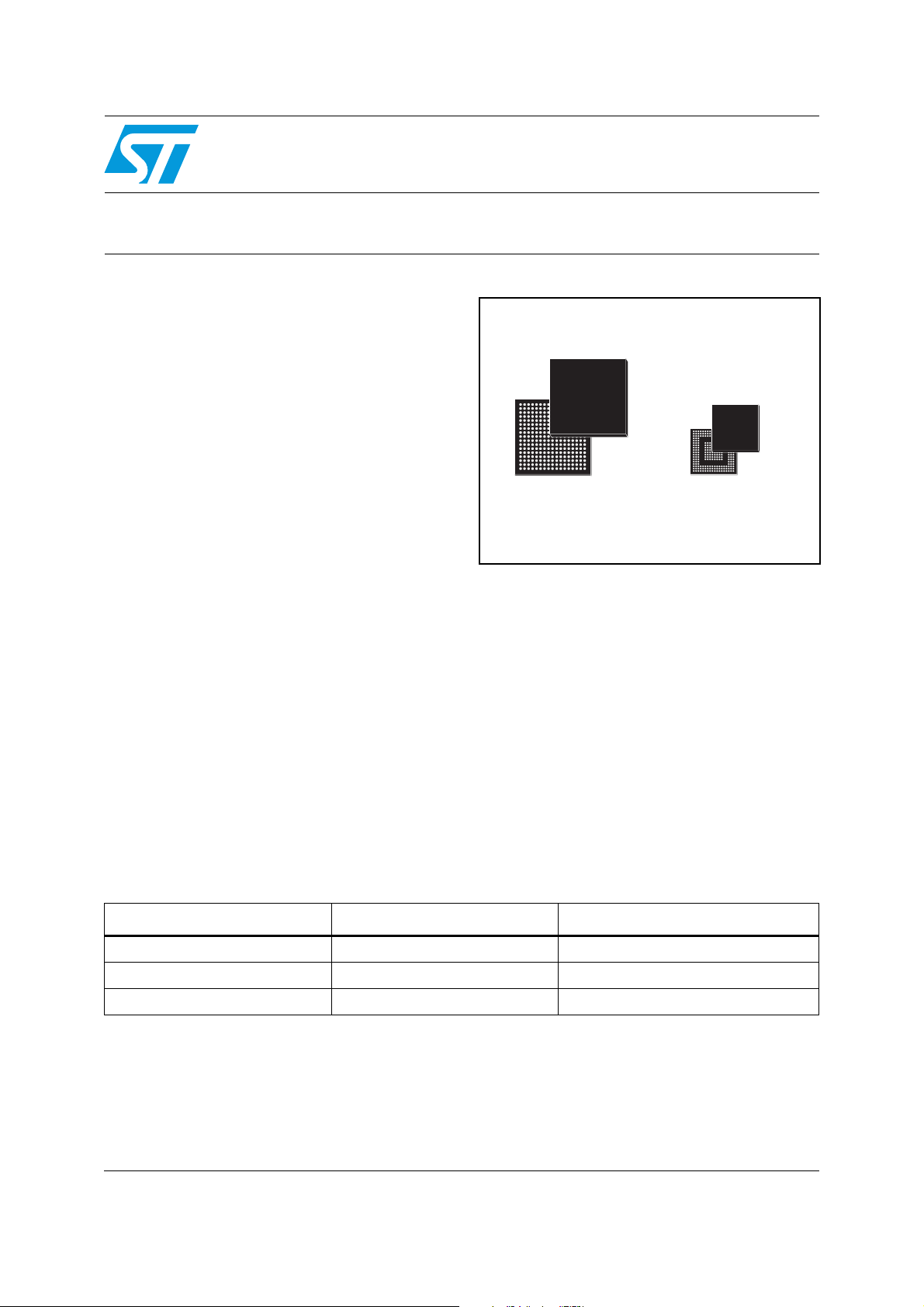
Sirius SDARS channel, service & source decoder
Features
■ 2 Satellite and 1 terrestrial signal demodulators
and decoders
■ Advanced DSP processor to implement PAC
audio decoder
■ Requires a single 17MHz clock reference; all
high-speed clock signals are derived using
on-chip PLL
■ Programmable I
audio sample rate (32K/48K Sample rates use
internal clocks, 44.1K Sample rate uses
external clock)
2
■ I
C master interface to control tuner and audio
DAC
■ External control through UART interface using
Sirius Standard Protocol (SSP) over RS-232
Analog to digital converters
■ Three internal 10 BIT A/D converters for
76.5MHZ if signals conversion
Low power technology
■ 1.2V, 90 µm technology
■ 2.5V capable I/OS
Table 1. Device summary
Part Number
2
S to support 32K/48K/44.1K
(1)
Package Packing
STA260
Data Brief
LFBGA289 VFBGA244
(15x15x1.4mm) (8x8x1.0mm)
Description
STA260 is a fully integrated 3rd generation
Baseband signal processor for Sirius Satellite
Digital Audio Radio Service (SDARS). It is
implemented using ST Micro's advanced 90 µm
CMOS090 technology.
It allows a highly efficient implementation of a
Sirius “SDARS Satellite Digital Audio Radio
Service” receiver when used with its companion
STA210 tuner ASIC.
STA260 is packaged in a Low profile Fine pitch
Ball Grid Array (LFBGA 15x15) and in Very thin
Fine pitch Ball Grid Array (VFBGA 8x8).
STA260 LFBGA289 Tray
STA260TR LFBGA289 Tape & reel
STA260-8x8 VFBGA244 Tray
1. This device is Pb-Free ECOPACK® see Chapter 3: Package information.
June 2007 Rev 1 1/7
For further information contact your local STMicroelectronics sales office.
www.st.com
7
Page 2

Application block diagram STA260
1 Application block diagram
Figure 1. Application block diagram
FLASH
1M x 16
STA210N
Tuner FE
IF
I2C
IFAGC
STA260
STA260
Baseband
Baseband
Processor
Processor
SDRAM
8Mbx8 or 16Mx8
Audio/I2S
Data
AC00244
2/7
Page 3
STA260 Electrical specifications
2 Electrical specifications
2.1 Absolute maximum ratings
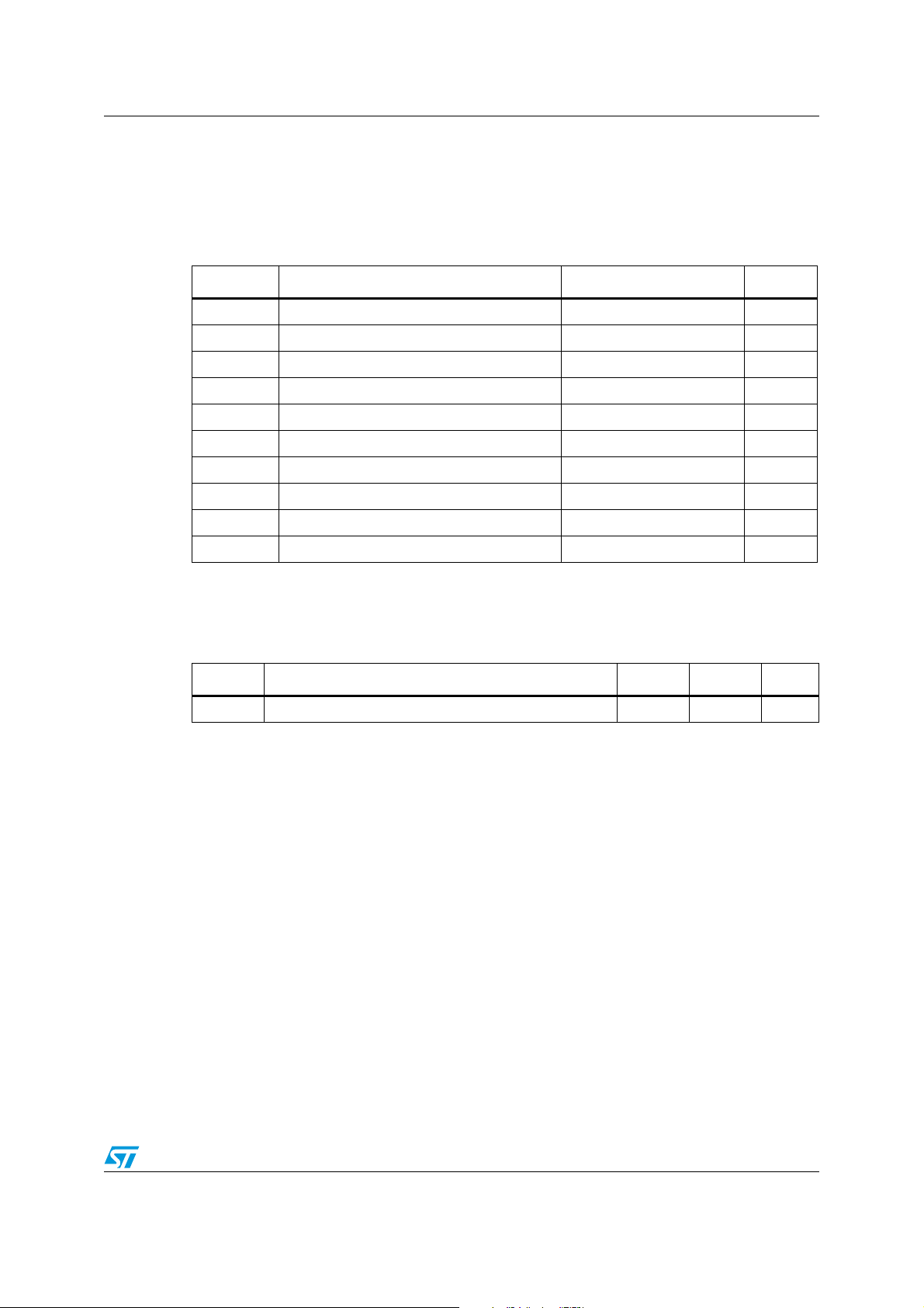
Table 2. Absolute maximum ratings
Symbol Parameter Value Unit
V
DD
V
DDIO
A
D_VDD
A
D_VDD2
A
PLL_VDD
V
V
T
stg
T
op
T
o
1.2V Power supply Voltage 1.32 V
2.5V Power Supply Voltage 2.75 V
1.2V Power supply Voltage 1.32 V
2.5V Power Supply Voltage 2.75 V
2.5V Power Supply Voltage 2.75 V
Voltage on input pin -0.5 to (V
i
Voltage on output pin -0.5 to (V
Storage Temperature -55 to +150 °C
Operative Ambient Temperature -40 to +85 °C
Operative Junction Temperature -40 to +125 °C
j
2.2 Thermal data
Table 3. Thermal data
Symbol Parameter LFBGA VFBGA Unit
R
th j-amb
1. According to JEDEC specification on a 4 layers board
Thermal resistance Junction to ambient
(1)
+ 0.5) V
DDIO
+ 0.5) V
DDIO
35 50 °C/W
3/7
Page 4
Package information STA260
3 Package information
In order to meet environmental requirements, ST offers these devices in ECOPACK®
packages. These packages have a Lead-free second level interconnect. The category of
second Level Interconnect is marked on the package and on the inner box label, in
compliance with JEDEC Standard JESD97. The maximum ratings related to soldering
conditions are also marked on the inner box label.
ECOPACK is an ST trademark. ECOPACK specifications are available at: www.st.com.
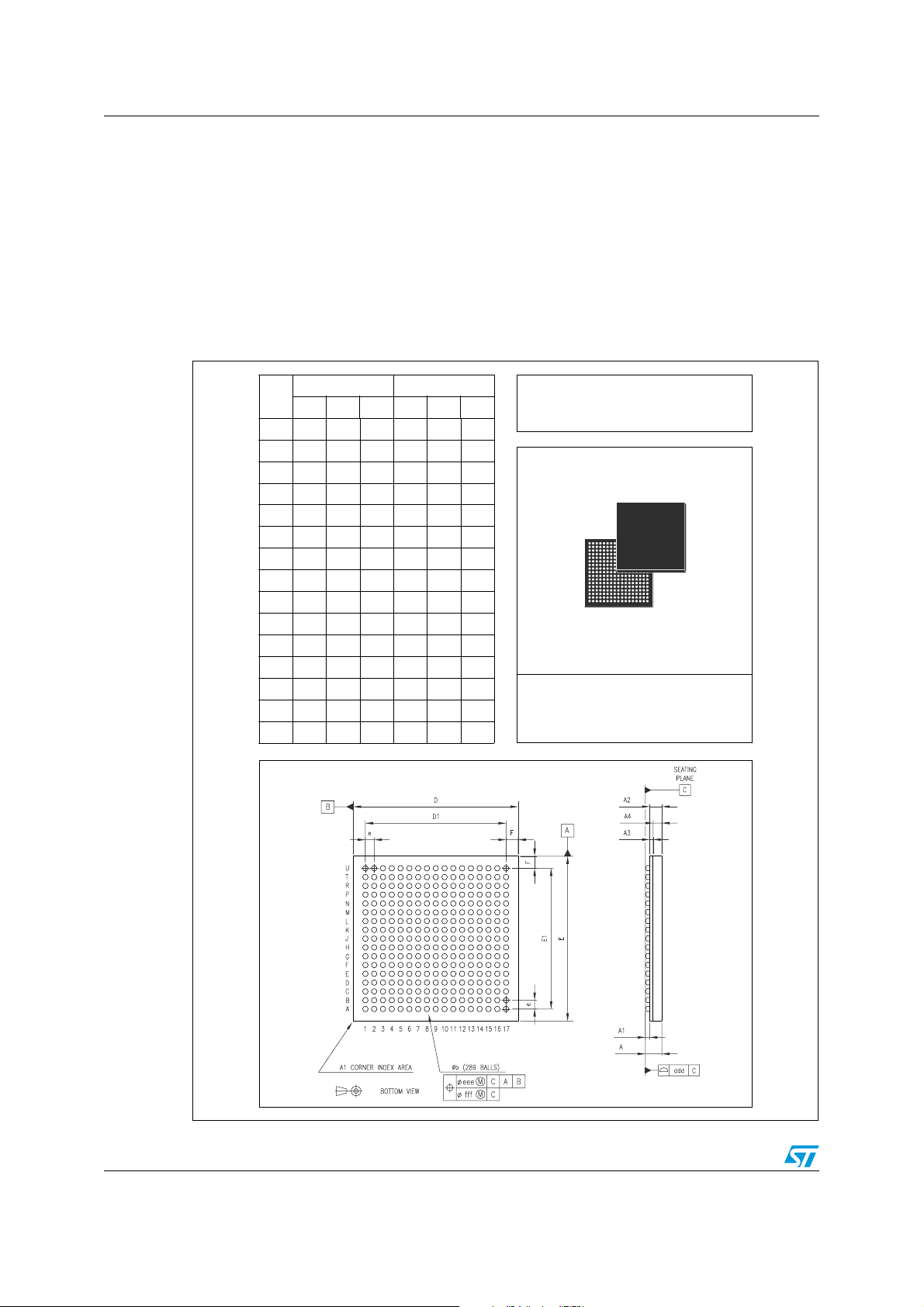
Figure 2. LFBGA (15x15x1.4mm 289 ball) mechanical data & package dimensions
DIM.
A 1.400 0.0551
A1 0.210 0.0083
A2 0.985 0.0387
A3 0.200 0.0078
A4 0.800 0.0315
b 0.350 0.400 0.450 0.0138 0.0157 0.0177
D 14.850 15.000 15.150 0.5846 0.5906 0.5965
D1 12.800 0.5039
E 14.850 15.000 15.150 0.5846 0.5906 0.5965
E1 12.800 0.5039
e 0.800 0.0315
F 1.100 0.0433
ddd 0.120 0.0047
eee 0.150 0.0059
fff 0.080 0.0031
mm inch
MIN. TYP. MAX. MIN. TYP. MAX.
OUTLINE AND
MECHANICAL DATA
Body: 15 x 15 x 1.4mm
LFBGA289
Low profile Fine Pitch Ball Grid Array
4/7
7963045 C
Page 5
STA260 Package information
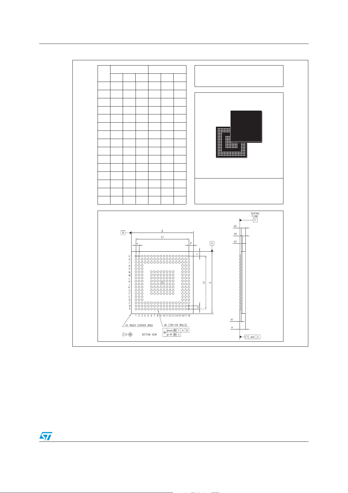
Figure 3. VFBGA (8x8x1.0mm 180+64 ball) mechanical data & package dimensions
DIM.
A 1.000 0.0394
A1 0.130 0.170 0.210 0.0051 0.0067 0.0083
A2 0.620 0.0244
A3 0.180 0.0071
A4 0.450 0.0177
b 0.220 0.260 0.300 0.0087 0.0102 0.0118
D 7.950 8.000 8.050 0.3130 0.3150 0.3169
D1 6.800 0.2677
E 7.950 8.000 8.050 0.3130 0.3150 0.3169
E1 6.800 0.2677
e 0.400 0.0157
F 0.600 0.0236
ddd 0.080 0.0031
eee 0.130 0.0051
fff 0.040 0.0016
mm inch
MIN. TYP. MAX. MIN. TYP. MAX.
OUTLINE AND
MECHANICAL DATA
Body: 8 x 8 x 1.0mm
VFBGA244
Very thin profile Fine Pitch Ball Grid Array
7520777 C
5/7
Page 6

Revision history STA260
4 Revision history
Table 4. Document revision history
Date Revision Changes
18-Jun-2007 1 Initial release.
6/7
Page 7

STA260
Please Read Carefully:
Information in this document is provided solely in connection with ST products. STMicroelectronics NV and its subsidiaries (“ST”) reserve the
right to make changes, corrections, modifications or improvements, to this document, and the products and services described herein at any
time, without notice.
All ST products are sold pursuant to ST’s terms and conditions of sale.
Purchasers are solely responsible for the choice, selection and use of the ST products and services described herein, and ST assumes no
liability whatsoever relating to the choice, selection or use of the ST products and services described herein.
No license, express or implied, by estoppel or otherwise, to any intellectual property rights is granted under this document. If any part of this
document refers to any third party products or services it shall not be deemed a license grant by ST for the use of such third party products
or services, or any intellectual property contained therein or considered as a warranty covering the use in any manner whatsoever of such
third party products or services or any intellectual property contained therein.
UNLESS OTHERWISE SET FORTH IN ST’S TERMS AND CONDITIONS OF SALE ST DISCLAIMS ANY EXPRESS OR IMPLIED
WARRANTY WITH RESPECT TO THE USE AND/OR SALE OF ST PRODUCTS INCLUDING WITHOUT LIMITATION IMPLIED
WARRANTIES OF MERCHANTABILITY, FITNESS FOR A PARTICULAR PURPOSE (AND THEIR EQUIVALENTS UNDER THE LAWS
OF ANY JURISDICTION), OR INFRINGEMENT OF ANY PATENT, COPYRIGHT OR OTHER INTELLECTUAL PROPERTY RIGHT.
UNLESS EXPRESSLY APPROVED IN WRITING BY AN AUTHORIZED ST REPRESENTATIVE, ST PRODUCTS ARE NOT
RECOMMENDED, AUTHORIZED OR WARRANTED FOR USE IN MILITARY, AIR CRAFT, SPACE, LIFE SAVING, OR LIFE SUSTAINING
APPLICATIONS, NOR IN PRODUCTS OR SYSTEMS WHERE FAILURE OR MALFUNCTION MAY RESULT IN PERSONAL INJURY,
DEATH, OR SEVERE PROPERTY OR ENVIRONMENTAL DAMAGE. ST PRODUCTS WHICH ARE NOT SPECIFIED AS "AUTOMOTIVE
GRADE" MAY ONLY BE USED IN AUTOMOTIVE APPLICATIONS AT USER’S OWN RISK.
Resale of ST products with provisions different from the statements and/or technical features set forth in this document shall immediately void
any warranty granted by ST for the ST product or service described herein and shall not create or extend in any manner whatsoever, any
liability of ST.
ST and the ST logo are trademarks or registered trademarks of ST in various countries.
Information in this document supersedes and replaces all information previously supplied.
The ST logo is a registered trademark of STMicroelectronics. All other names are the property of their respective owners.
© 2007 STMicroelectronics - All rights reserved
STMicroelectronics group of companies
Australia - Belgium - Brazil - Canada - China - Czech Republic - Finland - France - Germany - Hong Kong - India - Israel - Italy - Japan -
Malaysia - Malta - Morocco - Singapore - Spain - Sweden - Switzerland - United Kingdom - United States of America
www.st.com
7/7
 Loading...