

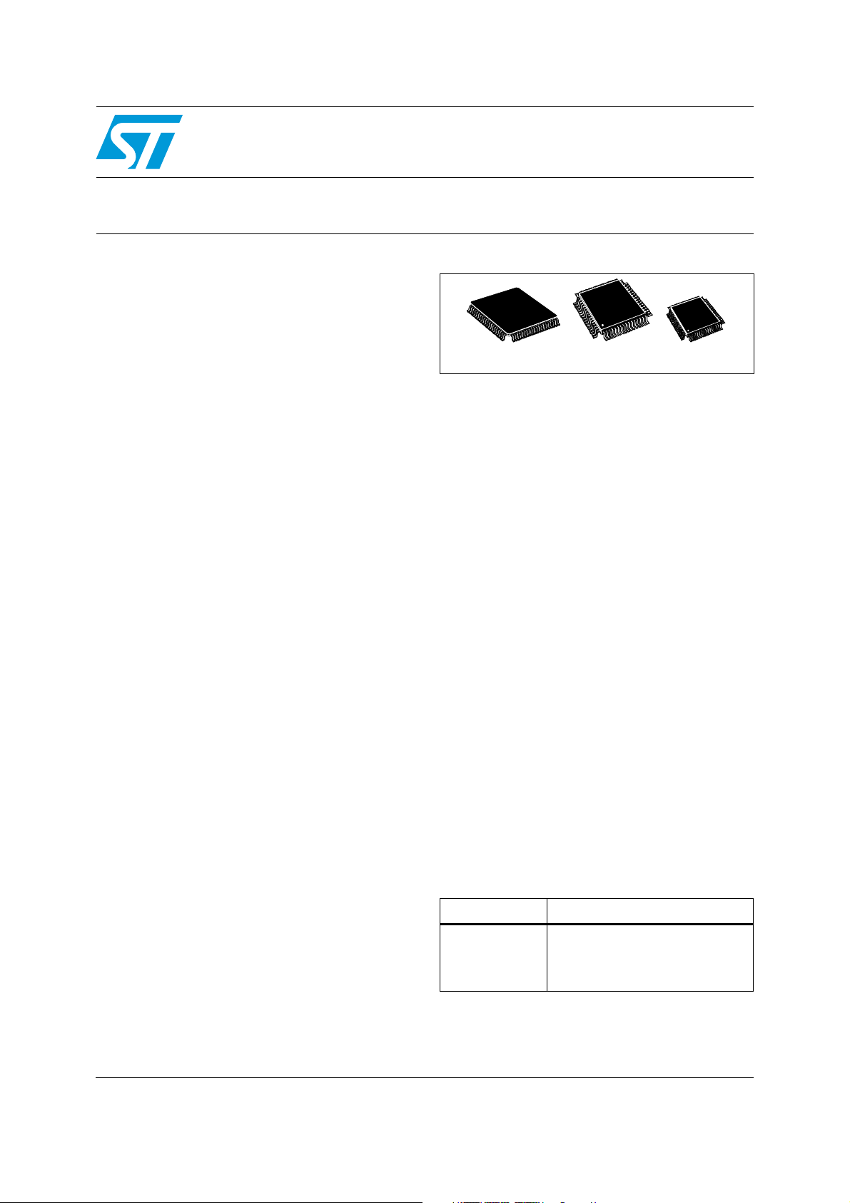
8-bit MCU for automotive with 32/60 Kbyte Flash/ROM,
LQFP80
14 x 14
LQFP64
10 x 10
LQFP64
14 x 14
ADC, 5 timers, SPI, SCI, I2C, CAN interface
Features
Memories
■ 32 to 60 Kbyte dual voltage High Density Flash
(HDFlash) or ROM with readout protection
capability. In-application programming and incircuit programming for HDFlash devices
■ 1 to 2 Kbyte RAM
■ HDFlash endurance: 100 cycles, data retention
20 years
Clock, reset and supply management
■ Enhanced low voltage supervisor (LVD) for
main supply and auxiliary voltage detector
(AVD) with interrupt capability
■ Clock sources: crystal/ceramic resonator
oscillators, internal RC oscillator and bypass
for external clock
■ PLL for 2x frequency multiplication
■ 4 power saving modes: Halt, Active Halt, Wait
and Slow
Interrupt management
■ Nested interrupt controller
■ 14 interrupt vectors plus TRAP and RESET
■ Top Level Interrupt (TLI) pin
■ 15 external interrupt lines (on 4 vectors)
Analog peripheral
■ 10-bit ADC with up to 16 input ports
Up to 64 I/O ports
■ 48 multifunctional bidirectional I/O lines
■ 34 alternate function lines
■ 16 high sink outputs
ST72521xx-Auto
5 timers
■ Main clock controller with Real-time base,
Beep and Clock-out capabilities
■ Configurable watchdog timer
■ Two 16-bit timers with 2 input captures, 2
output compares, external clock input on 1
timer, PWM and pulse generator modes
■ 8-bit PWM auto-reload timer with 2 input
captures, 4 PWM outputs, output compare and
time base interrupt, external clock with event
detector
4 communications interfaces
■ SPI synchronous serial interface
■ SCI asynchronous serial interface
2
■ I
C multimaster interface (SMbus V1.1
compliant)
■ CAN interface (2.0B passive)
Instruction set
■ 8-bit data manipulation
■ 63 basic instructions
■ 17 main addressing modes
■ 8x8 unsigned multiply instruction
Development tools
■ Full HW/SW development pkg, ICT capability
Table 1. Device summary
Reference Part number
ST72521R6-Auto
ST72521xx-Auto
ST72521R9-Auto
ST72521AR9-Auto
ST72521M9-Auto
July 2010 Doc ID 17660 Rev 1 1/276
www.st.com
1

Contents ST72521xx-Auto
Contents
1 Description . . . . . . . . . . . . . . . . . . . . . . . . . . . . . . . . . . . . . . . . . . . . . . . . 19
2 Package pinout and pin description . . . . . . . . . . . . . . . . . . . . . . . . . . . 21
2.1 Package pinout . . . . . . . . . . . . . . . . . . . . . . . . . . . . . . . . . . . . . . . . . . . . . 21
2.2 Pin description . . . . . . . . . . . . . . . . . . . . . . . . . . . . . . . . . . . . . . . . . . . . . 23
3 Register and memory map . . . . . . . . . . . . . . . . . . . . . . . . . . . . . . . . . . . 28
4 Flash program memory . . . . . . . . . . . . . . . . . . . . . . . . . . . . . . . . . . . . . 32
4.1 Introduction . . . . . . . . . . . . . . . . . . . . . . . . . . . . . . . . . . . . . . . . . . . . . . . 32
4.2 Main features . . . . . . . . . . . . . . . . . . . . . . . . . . . . . . . . . . . . . . . . . . . . . . 32
4.3 Structure . . . . . . . . . . . . . . . . . . . . . . . . . . . . . . . . . . . . . . . . . . . . . . . . . . 32
4.3.1 Readout protection . . . . . . . . . . . . . . . . . . . . . . . . . . . . . . . . . . . . . . . . 33
4.4 ICC interface . . . . . . . . . . . . . . . . . . . . . . . . . . . . . . . . . . . . . . . . . . . . . . 33
4.5 ICP (in-circuit programming) . . . . . . . . . . . . . . . . . . . . . . . . . . . . . . . . . . 34
4.6 IAP (in-application programming) . . . . . . . . . . . . . . . . . . . . . . . . . . . . . . . 35
4.7 Related documentation . . . . . . . . . . . . . . . . . . . . . . . . . . . . . . . . . . . . . . 35
4.8 Flash control/status register (FCSR) . . . . . . . . . . . . . . . . . . . . . . . . . . . . 35
5 Central processing unit (CPU) . . . . . . . . . . . . . . . . . . . . . . . . . . . . . . . . 36
5.1 Introduction . . . . . . . . . . . . . . . . . . . . . . . . . . . . . . . . . . . . . . . . . . . . . . . 36
5.2 Main features . . . . . . . . . . . . . . . . . . . . . . . . . . . . . . . . . . . . . . . . . . . . . . 36
5.3 CPU registers . . . . . . . . . . . . . . . . . . . . . . . . . . . . . . . . . . . . . . . . . . . . . . 36
5.3.1 Accumulator (A) . . . . . . . . . . . . . . . . . . . . . . . . . . . . . . . . . . . . . . . . . . . 37
5.3.2 Index registers (X and Y) . . . . . . . . . . . . . . . . . . . . . . . . . . . . . . . . . . . . 37
5.3.3 Program counter (PC) . . . . . . . . . . . . . . . . . . . . . . . . . . . . . . . . . . . . . . 37
5.3.4 Condition code (CC) register . . . . . . . . . . . . . . . . . . . . . . . . . . . . . . . . . 37
5.3.5 Stack pointer (SP) register . . . . . . . . . . . . . . . . . . . . . . . . . . . . . . . . . . . 38
6 Supply, reset and clock management . . . . . . . . . . . . . . . . . . . . . . . . . . 40
6.1 Introduction . . . . . . . . . . . . . . . . . . . . . . . . . . . . . . . . . . . . . . . . . . . . . . . 40
6.2 Main features . . . . . . . . . . . . . . . . . . . . . . . . . . . . . . . . . . . . . . . . . . . . . . 40
6.3 Phase locked loop . . . . . . . . . . . . . . . . . . . . . . . . . . . . . . . . . . . . . . . . . . 41
2/276 Doc ID 17660 Rev 1

ST72521xx-Auto Contents
6.4 Multi-oscillator (MO) . . . . . . . . . . . . . . . . . . . . . . . . . . . . . . . . . . . . . . . . . 41
6.5 Reset sequence manager (RSM) . . . . . . . . . . . . . . . . . . . . . . . . . . . . . . . 43
6.5.1 Introduction . . . . . . . . . . . . . . . . . . . . . . . . . . . . . . . . . . . . . . . . . . . . . . 43
6.5.2 Asynchronous external RESET pin . . . . . . . . . . . . . . . . . . . . . . . . . . . . 44
6.5.3 External power-on RESET . . . . . . . . . . . . . . . . . . . . . . . . . . . . . . . . . . . 44
6.5.4 Internal low voltage detector (LVD) RESET . . . . . . . . . . . . . . . . . . . . . . 44
6.5.5 Internal watchdog RESET . . . . . . . . . . . . . . . . . . . . . . . . . . . . . . . . . . . 45
6.6 System integrity management (SI) . . . . . . . . . . . . . . . . . . . . . . . . . . . . . . 46
6.6.1 Low voltage detector (LVD) . . . . . . . . . . . . . . . . . . . . . . . . . . . . . . . . . . 46
6.6.2 Auxiliary voltage detector (AVD) . . . . . . . . . . . . . . . . . . . . . . . . . . . . . . 47
6.6.3 Low power modes . . . . . . . . . . . . . . . . . . . . . . . . . . . . . . . . . . . . . . . . . 49
6.6.4 Interrupts . . . . . . . . . . . . . . . . . . . . . . . . . . . . . . . . . . . . . . . . . . . . . . . . 49
6.6.5 System Integrity (SI) Control/Status register (SICSR) . . . . . . . . . . . . . . 50
7 Interrupts . . . . . . . . . . . . . . . . . . . . . . . . . . . . . . . . . . . . . . . . . . . . . . . . . 52
7.1 Introduction . . . . . . . . . . . . . . . . . . . . . . . . . . . . . . . . . . . . . . . . . . . . . . . 52
7.2 Masking and processing flow . . . . . . . . . . . . . . . . . . . . . . . . . . . . . . . . . . 52
7.3 Interrupts and low power modes . . . . . . . . . . . . . . . . . . . . . . . . . . . . . . . 55
7.4 Concurrent and nested management . . . . . . . . . . . . . . . . . . . . . . . . . . . . 55
7.5 Interrupt register description . . . . . . . . . . . . . . . . . . . . . . . . . . . . . . . . . . 56
7.5.1 CPU CC register interrupt bits . . . . . . . . . . . . . . . . . . . . . . . . . . . . . . . . 56
7.5.2 Interrupt software priority registers (ISPRx) . . . . . . . . . . . . . . . . . . . . . . 57
7.6 External interrupts . . . . . . . . . . . . . . . . . . . . . . . . . . . . . . . . . . . . . . . . . . 60
7.6.1 I/O port interrupt sensitivity . . . . . . . . . . . . . . . . . . . . . . . . . . . . . . . . . . 60
7.6.2 External interrupt control register (EICR) . . . . . . . . . . . . . . . . . . . . . . . . 62
8 Power saving modes . . . . . . . . . . . . . . . . . . . . . . . . . . . . . . . . . . . . . . . . 65
8.1 Introduction . . . . . . . . . . . . . . . . . . . . . . . . . . . . . . . . . . . . . . . . . . . . . . . 65
8.2 Slow mode . . . . . . . . . . . . . . . . . . . . . . . . . . . . . . . . . . . . . . . . . . . . . . . . 65
8.3 Wait mode . . . . . . . . . . . . . . . . . . . . . . . . . . . . . . . . . . . . . . . . . . . . . . . . 66
8.4 Active Halt and Halt modes . . . . . . . . . . . . . . . . . . . . . . . . . . . . . . . . . . . 68
8.4.1 Active Halt mode . . . . . . . . . . . . . . . . . . . . . . . . . . . . . . . . . . . . . . . . . . 68
8.4.2 Halt mode . . . . . . . . . . . . . . . . . . . . . . . . . . . . . . . . . . . . . . . . . . . . . . . 70
9 I/O ports . . . . . . . . . . . . . . . . . . . . . . . . . . . . . . . . . . . . . . . . . . . . . . . . . . 73
9.1 Introduction . . . . . . . . . . . . . . . . . . . . . . . . . . . . . . . . . . . . . . . . . . . . . . . 73
Doc ID 17660 Rev 1 3/276

Contents ST72521xx-Auto
9.2 Functional description . . . . . . . . . . . . . . . . . . . . . . . . . . . . . . . . . . . . . . . 73
9.2.1 Input modes . . . . . . . . . . . . . . . . . . . . . . . . . . . . . . . . . . . . . . . . . . . . . . 73
9.2.2 Output modes . . . . . . . . . . . . . . . . . . . . . . . . . . . . . . . . . . . . . . . . . . . . 74
9.2.3 Alternate functions . . . . . . . . . . . . . . . . . . . . . . . . . . . . . . . . . . . . . . . . . 74
9.3 I/O port implementation . . . . . . . . . . . . . . . . . . . . . . . . . . . . . . . . . . . . . . 77
9.4 Low power modes . . . . . . . . . . . . . . . . . . . . . . . . . . . . . . . . . . . . . . . . . . 78
9.5 Interrupts . . . . . . . . . . . . . . . . . . . . . . . . . . . . . . . . . . . . . . . . . . . . . . . . . 78
10 Watchdog timer (WDG) . . . . . . . . . . . . . . . . . . . . . . . . . . . . . . . . . . . . . . 80
10.1 Introduction . . . . . . . . . . . . . . . . . . . . . . . . . . . . . . . . . . . . . . . . . . . . . . . 80
10.2 Main features . . . . . . . . . . . . . . . . . . . . . . . . . . . . . . . . . . . . . . . . . . . . . . 80
10.3 Functional description . . . . . . . . . . . . . . . . . . . . . . . . . . . . . . . . . . . . . . . 80
10.4 How to program the watchdog timeout . . . . . . . . . . . . . . . . . . . . . . . . . . . 81
10.5 Low power modes . . . . . . . . . . . . . . . . . . . . . . . . . . . . . . . . . . . . . . . . . . 83
10.6 Hardware watchdog option . . . . . . . . . . . . . . . . . . . . . . . . . . . . . . . . . . . . 83
10.7 Using Halt mode with the WDG (WDGHALT option) . . . . . . . . . . . . . . . . 83
10.8 Interrupts . . . . . . . . . . . . . . . . . . . . . . . . . . . . . . . . . . . . . . . . . . . . . . . . . 83
10.9 Register description . . . . . . . . . . . . . . . . . . . . . . . . . . . . . . . . . . . . . . . . . 84
10.9.1 Control register (WDGCR) . . . . . . . . . . . . . . . . . . . . . . . . . . . . . . . . . . . 84
11 Main clock controller with real-time clock and beeper (MCC/RTC) . . 85
11.1 Introduction . . . . . . . . . . . . . . . . . . . . . . . . . . . . . . . . . . . . . . . . . . . . . . . 85
11.2 Programmable CPU clock prescaler . . . . . . . . . . . . . . . . . . . . . . . . . . . . 85
11.3 Clock-out capability . . . . . . . . . . . . . . . . . . . . . . . . . . . . . . . . . . . . . . . . . 85
11.4 Real-time clock timer (RTC) . . . . . . . . . . . . . . . . . . . . . . . . . . . . . . . . . . . 85
11.5 Beeper . . . . . . . . . . . . . . . . . . . . . . . . . . . . . . . . . . . . . . . . . . . . . . . . . . . 85
11.6 Low power modes . . . . . . . . . . . . . . . . . . . . . . . . . . . . . . . . . . . . . . . . . . 86
11.7 Interrupts . . . . . . . . . . . . . . . . . . . . . . . . . . . . . . . . . . . . . . . . . . . . . . . . . 86
11.8 Main clock controller registers . . . . . . . . . . . . . . . . . . . . . . . . . . . . . . . . . 87
11.8.1 MCC control/status register (MCCSR) . . . . . . . . . . . . . . . . . . . . . . . . . . 87
11.8.2 MCC beep control register (MCCBCR) . . . . . . . . . . . . . . . . . . . . . . . . . 88
12 PWM auto-reload timer (ART) . . . . . . . . . . . . . . . . . . . . . . . . . . . . . . . . 90
12.1 Introduction . . . . . . . . . . . . . . . . . . . . . . . . . . . . . . . . . . . . . . . . . . . . . . . 90
12.2 Functional description . . . . . . . . . . . . . . . . . . . . . . . . . . . . . . . . . . . . . . . 91
4/276 Doc ID 17660 Rev 1

ST72521xx-Auto Contents
12.2.1 Counter . . . . . . . . . . . . . . . . . . . . . . . . . . . . . . . . . . . . . . . . . . . . . . . . . 91
12.2.2 Counter clock and prescaler . . . . . . . . . . . . . . . . . . . . . . . . . . . . . . . . . 91
12.2.3 Counter and prescaler initialization . . . . . . . . . . . . . . . . . . . . . . . . . . . . 91
12.2.4 Output compare control . . . . . . . . . . . . . . . . . . . . . . . . . . . . . . . . . . . . . 91
12.2.5 Independent PWM signal generation . . . . . . . . . . . . . . . . . . . . . . . . . . . 92
12.2.6 Output compare and time base interrupt . . . . . . . . . . . . . . . . . . . . . . . . 93
12.2.7 External clock and event detector mode . . . . . . . . . . . . . . . . . . . . . . . . 93
12.2.8 Input capture function . . . . . . . . . . . . . . . . . . . . . . . . . . . . . . . . . . . . . . 94
12.2.9 External interrupt capability . . . . . . . . . . . . . . . . . . . . . . . . . . . . . . . . . . 95
12.3 ART registers . . . . . . . . . . . . . . . . . . . . . . . . . . . . . . . . . . . . . . . . . . . . . . 96
12.3.1 Control/status register (ARTCSR) . . . . . . . . . . . . . . . . . . . . . . . . . . . . . 96
12.3.2 Counter access register (ARTCAR) . . . . . . . . . . . . . . . . . . . . . . . . . . . . 97
12.3.3 Auto-reload register (ARTARR) . . . . . . . . . . . . . . . . . . . . . . . . . . . . . . . 97
12.3.4 PWM control register (PWMCR) . . . . . . . . . . . . . . . . . . . . . . . . . . . . . . 98
12.3.5 Duty cycle registers (PWMDCRx) . . . . . . . . . . . . . . . . . . . . . . . . . . . . . 99
12.3.6 Input capture control / status register (ARTICCSR) . . . . . . . . . . . . . . . . 99
12.3.7 Input capture registers (ARTICRx) . . . . . . . . . . . . . . . . . . . . . . . . . . . . 100
13 16-bit timer . . . . . . . . . . . . . . . . . . . . . . . . . . . . . . . . . . . . . . . . . . . . . . . 101
13.1 Introduction . . . . . . . . . . . . . . . . . . . . . . . . . . . . . . . . . . . . . . . . . . . . . . 101
13.2 Main features . . . . . . . . . . . . . . . . . . . . . . . . . . . . . . . . . . . . . . . . . . . . . 101
13.3 Functional description . . . . . . . . . . . . . . . . . . . . . . . . . . . . . . . . . . . . . . 102
13.3.1 Counter . . . . . . . . . . . . . . . . . . . . . . . . . . . . . . . . . . . . . . . . . . . . . . . . 102
13.3.2 External clock . . . . . . . . . . . . . . . . . . . . . . . . . . . . . . . . . . . . . . . . . . . 105
13.3.3 Input capture . . . . . . . . . . . . . . . . . . . . . . . . . . . . . . . . . . . . . . . . . . . . 106
13.3.4 Output compare . . . . . . . . . . . . . . . . . . . . . . . . . . . . . . . . . . . . . . . . . . 108
13.3.5 Forced compare output capability . . . . . . . . . . . . . . . . . . . . . . . . . . . . 109
13.3.6 One Pulse mode . . . . . . . . . . . . . . . . . . . . . . . . . . . . . . . . . . . . . . . . . 111
13.3.7 Pulse width modulation mode . . . . . . . . . . . . . . . . . . . . . . . . . . . . . . . 113
13.4 Low power modes . . . . . . . . . . . . . . . . . . . . . . . . . . . . . . . . . . . . . . . . . 115
13.5 Interrupts . . . . . . . . . . . . . . . . . . . . . . . . . . . . . . . . . . . . . . . . . . . . . . . . 115
13.6 Summary of timer modes . . . . . . . . . . . . . . . . . . . . . . . . . . . . . . . . . . . . 115
13.7 16-bit timer registers . . . . . . . . . . . . . . . . . . . . . . . . . . . . . . . . . . . . . . . . 116
13.7.1 Control register 1 (CR1) . . . . . . . . . . . . . . . . . . . . . . . . . . . . . . . . . . . . 116
13.7.2 Control register 2 (CR2) . . . . . . . . . . . . . . . . . . . . . . . . . . . . . . . . . . . . 117
13.7.3 Control/status register (CSR) . . . . . . . . . . . . . . . . . . . . . . . . . . . . . . . . 118
Doc ID 17660 Rev 1 5/276

Contents ST72521xx-Auto
13.7.4 Input capture 1 high register (IC1HR) . . . . . . . . . . . . . . . . . . . . . . . . . 119
13.7.5 Input capture 1 low register (IC1LR) . . . . . . . . . . . . . . . . . . . . . . . . . . 120
13.7.6 Output compare 1 high register (OC1HR) . . . . . . . . . . . . . . . . . . . . . . 120
13.7.7 Output compare 1 low register (OC1LR) . . . . . . . . . . . . . . . . . . . . . . . 120
13.7.8 Output compare 2 high register (OC2HR) . . . . . . . . . . . . . . . . . . . . . . 120
13.7.9 Output compare 2 low register (OC2LR) . . . . . . . . . . . . . . . . . . . . . . . 121
13.7.10 Counter high register (CHR) . . . . . . . . . . . . . . . . . . . . . . . . . . . . . . . . 121
13.7.11 Counter low register (CLR) . . . . . . . . . . . . . . . . . . . . . . . . . . . . . . . . . 121
13.7.12 Alternate counter high register (ACHR) . . . . . . . . . . . . . . . . . . . . . . . . 121
13.7.13 Alternate counter low register (ACLR) . . . . . . . . . . . . . . . . . . . . . . . . . 122
13.7.14 Input capture 2 high register (IC2HR) . . . . . . . . . . . . . . . . . . . . . . . . . 122
13.7.15 Input capture 2 low register (IC2LR) . . . . . . . . . . . . . . . . . . . . . . . . . . 122
14 Serial peripheral interface (SPI) . . . . . . . . . . . . . . . . . . . . . . . . . . . . . . 124
14.1 Introduction . . . . . . . . . . . . . . . . . . . . . . . . . . . . . . . . . . . . . . . . . . . . . . 124
14.2 Main features . . . . . . . . . . . . . . . . . . . . . . . . . . . . . . . . . . . . . . . . . . . . . 124
14.3 General description . . . . . . . . . . . . . . . . . . . . . . . . . . . . . . . . . . . . . . . . 124
14.3.1 Functional description . . . . . . . . . . . . . . . . . . . . . . . . . . . . . . . . . . . . . 125
14.3.2 Slave select management . . . . . . . . . . . . . . . . . . . . . . . . . . . . . . . . . . 126
14.3.3 Master mode operation . . . . . . . . . . . . . . . . . . . . . . . . . . . . . . . . . . . . 127
14.3.4 Master mode transmit sequence . . . . . . . . . . . . . . . . . . . . . . . . . . . . . 128
14.3.5 Slave mode operation . . . . . . . . . . . . . . . . . . . . . . . . . . . . . . . . . . . . . 128
14.3.6 Slave mode transmit sequence . . . . . . . . . . . . . . . . . . . . . . . . . . . . . . 128
14.4 Clock phase and clock polarity . . . . . . . . . . . . . . . . . . . . . . . . . . . . . . . . 129
14.5 Error flags . . . . . . . . . . . . . . . . . . . . . . . . . . . . . . . . . . . . . . . . . . . . . . . . 131
14.5.1 Master mode fault (MODF) . . . . . . . . . . . . . . . . . . . . . . . . . . . . . . . . . 131
14.5.2 Overrun condition (OVR) . . . . . . . . . . . . . . . . . . . . . . . . . . . . . . . . . . . 131
14.5.3 Write collision error (WCOL) . . . . . . . . . . . . . . . . . . . . . . . . . . . . . . . . 131
14.5.4 Single master systems . . . . . . . . . . . . . . . . . . . . . . . . . . . . . . . . . . . . . 132
14.6 Low power modes . . . . . . . . . . . . . . . . . . . . . . . . . . . . . . . . . . . . . . . . . 133
14.6.1 Using the SPI to wake up the MCU from Halt mode . . . . . . . . . . . . . . 133
14.7 Interrupts . . . . . . . . . . . . . . . . . . . . . . . . . . . . . . . . . . . . . . . . . . . . . . . . 133
14.8 SPI registers . . . . . . . . . . . . . . . . . . . . . . . . . . . . . . . . . . . . . . . . . . . . . . 134
14.8.1 Control register (SPICR) . . . . . . . . . . . . . . . . . . . . . . . . . . . . . . . . . . . 134
14.8.2 Control/status register (SPICSR) . . . . . . . . . . . . . . . . . . . . . . . . . . . . . 135
14.8.3 Data I/O register (SPIDR) . . . . . . . . . . . . . . . . . . . . . . . . . . . . . . . . . . 136
6/276 Doc ID 17660 Rev 1

ST72521xx-Auto Contents
15 Serial communications interface (SCI) . . . . . . . . . . . . . . . . . . . . . . . . 138
15.1 Introduction . . . . . . . . . . . . . . . . . . . . . . . . . . . . . . . . . . . . . . . . . . . . . . 138
15.2 Main features . . . . . . . . . . . . . . . . . . . . . . . . . . . . . . . . . . . . . . . . . . . . . 138
15.3 General description . . . . . . . . . . . . . . . . . . . . . . . . . . . . . . . . . . . . . . . . 139
15.4 Functional description . . . . . . . . . . . . . . . . . . . . . . . . . . . . . . . . . . . . . . 141
15.4.1 Serial data format . . . . . . . . . . . . . . . . . . . . . . . . . . . . . . . . . . . . . . . . 141
15.4.2 Transmitter . . . . . . . . . . . . . . . . . . . . . . . . . . . . . . . . . . . . . . . . . . . . . . 142
15.4.3 Receiver . . . . . . . . . . . . . . . . . . . . . . . . . . . . . . . . . . . . . . . . . . . . . . . . 143
15.5 Low power modes . . . . . . . . . . . . . . . . . . . . . . . . . . . . . . . . . . . . . . . . . 149
15.6 Interrupts . . . . . . . . . . . . . . . . . . . . . . . . . . . . . . . . . . . . . . . . . . . . . . . . 149
15.7 SCI registers . . . . . . . . . . . . . . . . . . . . . . . . . . . . . . . . . . . . . . . . . . . . . . 150
15.7.1 Status register (SCISR) . . . . . . . . . . . . . . . . . . . . . . . . . . . . . . . . . . . . 150
15.7.2 Control register 1 (SCICR1) . . . . . . . . . . . . . . . . . . . . . . . . . . . . . . . . . 152
15.7.3 Control register 2 (SCICR2) . . . . . . . . . . . . . . . . . . . . . . . . . . . . . . . . . 153
15.7.4 Data register (SCIDR) . . . . . . . . . . . . . . . . . . . . . . . . . . . . . . . . . . . . . 154
15.7.5 Baud rate register (SCIBRR) . . . . . . . . . . . . . . . . . . . . . . . . . . . . . . . . 154
15.7.6 Extended receive prescaler division register (SCIERPR) . . . . . . . . . . 155
15.7.7 Extended transmit prescaler division register (SCIETPR) . . . . . . . . . . 156
16 I2C bus interface (I2C) . . . . . . . . . . . . . . . . . . . . . . . . . . . . . . . . . . . . . 158
16.1 Introduction . . . . . . . . . . . . . . . . . . . . . . . . . . . . . . . . . . . . . . . . . . . . . . 158
16.2 Main features . . . . . . . . . . . . . . . . . . . . . . . . . . . . . . . . . . . . . . . . . . . . . 158
16.2.1 I2C master features . . . . . . . . . . . . . . . . . . . . . . . . . . . . . . . . . . . . . . . 158
16.2.2 I2C slave features . . . . . . . . . . . . . . . . . . . . . . . . . . . . . . . . . . . . . . . . 158
16.3 General description . . . . . . . . . . . . . . . . . . . . . . . . . . . . . . . . . . . . . . . . 159
16.3.1 Mode selection . . . . . . . . . . . . . . . . . . . . . . . . . . . . . . . . . . . . . . . . . . . 159
16.3.2 Communication flow . . . . . . . . . . . . . . . . . . . . . . . . . . . . . . . . . . . . . . . 159
16.3.3 SDA/SCL line control . . . . . . . . . . . . . . . . . . . . . . . . . . . . . . . . . . . . . . 160
16.4 Functional description . . . . . . . . . . . . . . . . . . . . . . . . . . . . . . . . . . . . . . 161
16.4.1 Slave mode . . . . . . . . . . . . . . . . . . . . . . . . . . . . . . . . . . . . . . . . . . . . . 161
16.4.2 Master mode . . . . . . . . . . . . . . . . . . . . . . . . . . . . . . . . . . . . . . . . . . . . 162
16.5 Low power modes . . . . . . . . . . . . . . . . . . . . . . . . . . . . . . . . . . . . . . . . . 166
16.6 Interrupts . . . . . . . . . . . . . . . . . . . . . . . . . . . . . . . . . . . . . . . . . . . . . . . . 166
16.7 Register description . . . . . . . . . . . . . . . . . . . . . . . . . . . . . . . . . . . . . . . . 167
16.7.1 I2C control register (CR) . . . . . . . . . . . . . . . . . . . . . . . . . . . . . . . . . . . 167
Doc ID 17660 Rev 1 7/276

Contents ST72521xx-Auto
16.7.2 I2C status register 1 (SR1) . . . . . . . . . . . . . . . . . . . . . . . . . . . . . . . . . 168
16.7.3 I2C status register 2 (SR2) . . . . . . . . . . . . . . . . . . . . . . . . . . . . . . . . . 170
16.7.4 I2C clock control register (CCR) . . . . . . . . . . . . . . . . . . . . . . . . . . . . . 171
16.7.5 I2C data register (DR) . . . . . . . . . . . . . . . . . . . . . . . . . . . . . . . . . . . . . 172
16.7.6 I2C own address register (OAR1) . . . . . . . . . . . . . . . . . . . . . . . . . . . . 172
16.7.7 I2C own address register (OAR2) . . . . . . . . . . . . . . . . . . . . . . . . . . . . 173
17 Controller area network (CAN) . . . . . . . . . . . . . . . . . . . . . . . . . . . . . . . 175
17.1 Introduction . . . . . . . . . . . . . . . . . . . . . . . . . . . . . . . . . . . . . . . . . . . . . . 175
17.2 Main features . . . . . . . . . . . . . . . . . . . . . . . . . . . . . . . . . . . . . . . . . . . . . 176
17.3 Functional description . . . . . . . . . . . . . . . . . . . . . . . . . . . . . . . . . . . . . . 176
17.3.1 Frame formats . . . . . . . . . . . . . . . . . . . . . . . . . . . . . . . . . . . . . . . . . . . 176
17.3.2 Hardware blocks . . . . . . . . . . . . . . . . . . . . . . . . . . . . . . . . . . . . . . . . . 177
17.3.3 Modes of operation . . . . . . . . . . . . . . . . . . . . . . . . . . . . . . . . . . . . . . . 179
17.3.4 Bit timing logic . . . . . . . . . . . . . . . . . . . . . . . . . . . . . . . . . . . . . . . . . . . 181
17.4 Register description . . . . . . . . . . . . . . . . . . . . . . . . . . . . . . . . . . . . . . . . 182
17.4.1 General purpose registers . . . . . . . . . . . . . . . . . . . . . . . . . . . . . . . . . . 182
17.4.2 Paged registers . . . . . . . . . . . . . . . . . . . . . . . . . . . . . . . . . . . . . . . . . . 187
17.5 List of CAN cell limitations . . . . . . . . . . . . . . . . . . . . . . . . . . . . . . . . . . . 196
17.5.1 Omitted SOF bit . . . . . . . . . . . . . . . . . . . . . . . . . . . . . . . . . . . . . . . . . . 196
17.5.2 CPU write access (more than one cycle) corrupts CAN frame . . . . . . 196
17.5.3 Unexpected message transmission . . . . . . . . . . . . . . . . . . . . . . . . . . . 197
17.5.4 WKPS functionality . . . . . . . . . . . . . . . . . . . . . . . . . . . . . . . . . . . . . . . 202
17.5.5 Bus-off state not entered . . . . . . . . . . . . . . . . . . . . . . . . . . . . . . . . . . . 203
18 10-bit A/D converter (ADC) . . . . . . . . . . . . . . . . . . . . . . . . . . . . . . . . . . 205
18.1 Introduction . . . . . . . . . . . . . . . . . . . . . . . . . . . . . . . . . . . . . . . . . . . . . . 205
18.2 Main features . . . . . . . . . . . . . . . . . . . . . . . . . . . . . . . . . . . . . . . . . . . . . 205
18.3 Functional description . . . . . . . . . . . . . . . . . . . . . . . . . . . . . . . . . . . . . . 206
18.3.1 A/D converter configuration . . . . . . . . . . . . . . . . . . . . . . . . . . . . . . . . . 206
18.3.2 Starting the conversion . . . . . . . . . . . . . . . . . . . . . . . . . . . . . . . . . . . . 206
18.3.3 Changing the conversion channel . . . . . . . . . . . . . . . . . . . . . . . . . . . . 207
18.4 Low power modes . . . . . . . . . . . . . . . . . . . . . . . . . . . . . . . . . . . . . . . . . 207
18.5 Interrupts . . . . . . . . . . . . . . . . . . . . . . . . . . . . . . . . . . . . . . . . . . . . . . . . 207
18.6 ADC registers . . . . . . . . . . . . . . . . . . . . . . . . . . . . . . . . . . . . . . . . . . . . . 207
18.6.1 Control/status register (ADCCSR) . . . . . . . . . . . . . . . . . . . . . . . . . . . . 207
8/276 Doc ID 17660 Rev 1

ST72521xx-Auto Contents
18.6.2 Data register (ADCDRH) . . . . . . . . . . . . . . . . . . . . . . . . . . . . . . . . . . . 208
18.6.3 Data register (ADCDRL) . . . . . . . . . . . . . . . . . . . . . . . . . . . . . . . . . . . 209
18.6.4 ADC register map and reset values . . . . . . . . . . . . . . . . . . . . . . . . . . . 209
19 Instruction set . . . . . . . . . . . . . . . . . . . . . . . . . . . . . . . . . . . . . . . . . . . . 210
19.1 CPU addressing modes . . . . . . . . . . . . . . . . . . . . . . . . . . . . . . . . . . . . . 210
19.1.1 Inherent . . . . . . . . . . . . . . . . . . . . . . . . . . . . . . . . . . . . . . . . . . . . . . . . 211
19.1.2 Immediate . . . . . . . . . . . . . . . . . . . . . . . . . . . . . . . . . . . . . . . . . . . . . . 212
19.1.3 Direct . . . . . . . . . . . . . . . . . . . . . . . . . . . . . . . . . . . . . . . . . . . . . . . . . . 212
19.1.4 Indexed (no offset, short, long) . . . . . . . . . . . . . . . . . . . . . . . . . . . . . . 212
19.1.5 Indirect (short, long) . . . . . . . . . . . . . . . . . . . . . . . . . . . . . . . . . . . . . . . 213
19.1.6 Indirect Indexed (Short, Long) . . . . . . . . . . . . . . . . . . . . . . . . . . . . . . . 213
19.1.7 Relative (Direct, Indirect) . . . . . . . . . . . . . . . . . . . . . . . . . . . . . . . . . . . 214
19.2 Instruction groups . . . . . . . . . . . . . . . . . . . . . . . . . . . . . . . . . . . . . . . . . . 214
19.2.1 Using a prebyte . . . . . . . . . . . . . . . . . . . . . . . . . . . . . . . . . . . . . . . . . . 215
20 Electrical characteristics . . . . . . . . . . . . . . . . . . . . . . . . . . . . . . . . . . . 218
20.1 Parameter conditions . . . . . . . . . . . . . . . . . . . . . . . . . . . . . . . . . . . . . . . 218
20.1.1 Minimum and maximum values . . . . . . . . . . . . . . . . . . . . . . . . . . . . . . 218
20.1.2 Typical values . . . . . . . . . . . . . . . . . . . . . . . . . . . . . . . . . . . . . . . . . . . . 218
20.1.3 Typical curves . . . . . . . . . . . . . . . . . . . . . . . . . . . . . . . . . . . . . . . . . . . 218
20.1.4 Loading capacitor . . . . . . . . . . . . . . . . . . . . . . . . . . . . . . . . . . . . . . . . 218
20.1.5 Pin input voltage . . . . . . . . . . . . . . . . . . . . . . . . . . . . . . . . . . . . . . . . . 218
20.2 Absolute maximum ratings . . . . . . . . . . . . . . . . . . . . . . . . . . . . . . . . . . . 219
20.2.1 Voltage characteristics . . . . . . . . . . . . . . . . . . . . . . . . . . . . . . . . . . . . . 219
20.2.2 Current characteristics . . . . . . . . . . . . . . . . . . . . . . . . . . . . . . . . . . . . . 220
20.2.3 Thermal characteristics . . . . . . . . . . . . . . . . . . . . . . . . . . . . . . . . . . . . 220
20.3 Operating conditions . . . . . . . . . . . . . . . . . . . . . . . . . . . . . . . . . . . . . . . 221
20.3.1 General operating conditions . . . . . . . . . . . . . . . . . . . . . . . . . . . . . . . . 221
20.3.2 Operating conditions with low voltage detector (LVD) . . . . . . . . . . . . . 222
20.3.3 Auxiliary voltage detector (AVD) thresholds . . . . . . . . . . . . . . . . . . . . . 222
20.3.4 External voltage detector (EVD) thresholds . . . . . . . . . . . . . . . . . . . . . 223
20.4 Supply current characteristics . . . . . . . . . . . . . . . . . . . . . . . . . . . . . . . . 224
20.4.1 Current consumption . . . . . . . . . . . . . . . . . . . . . . . . . . . . . . . . . . . . . . 224
20.4.2 Supply and clock managers . . . . . . . . . . . . . . . . . . . . . . . . . . . . . . . . . 226
20.4.3 On-chip peripherals . . . . . . . . . . . . . . . . . . . . . . . . . . . . . . . . . . . . . . . 227
Doc ID 17660 Rev 1 9/276

Contents ST72521xx-Auto
20.5 Clock and timing characteristics . . . . . . . . . . . . . . . . . . . . . . . . . . . . . . . 228
20.5.1 General timings . . . . . . . . . . . . . . . . . . . . . . . . . . . . . . . . . . . . . . . . . . 228
20.5.2 External clock source . . . . . . . . . . . . . . . . . . . . . . . . . . . . . . . . . . . . . . 228
20.5.3 Crystal and ceramic resonator oscillators . . . . . . . . . . . . . . . . . . . . . . 229
20.5.4 RC oscillators . . . . . . . . . . . . . . . . . . . . . . . . . . . . . . . . . . . . . . . . . . . . 230
20.5.5 PLL characteristics . . . . . . . . . . . . . . . . . . . . . . . . . . . . . . . . . . . . . . . 231
20.6 Memory characteristics . . . . . . . . . . . . . . . . . . . . . . . . . . . . . . . . . . . . . 232
20.6.1 RAM and hardware registers . . . . . . . . . . . . . . . . . . . . . . . . . . . . . . . . 232
20.6.2 Flash memory . . . . . . . . . . . . . . . . . . . . . . . . . . . . . . . . . . . . . . . . . . . 232
20.7 EMC (electromagnetic compatibility) characteristics . . . . . . . . . . . . . . . 233
20.7.1 Functional EMS (electromagnetic susceptibility) . . . . . . . . . . . . . . . . . 233
20.7.2 EMI (electromagnetic interference) . . . . . . . . . . . . . . . . . . . . . . . . . . . 234
20.7.3 Absolute maximum ratings (electrical sensitivity) . . . . . . . . . . . . . . . . 235
20.8 I/O port pin characteristics . . . . . . . . . . . . . . . . . . . . . . . . . . . . . . . . . . . 236
20.8.1 General characteristics . . . . . . . . . . . . . . . . . . . . . . . . . . . . . . . . . . . . 236
20.8.2 Output driving current . . . . . . . . . . . . . . . . . . . . . . . . . . . . . . . . . . . . . 237
20.9 Control pin characteristics . . . . . . . . . . . . . . . . . . . . . . . . . . . . . . . . . . . 240
20.9.1 Asynchronous RESET pin . . . . . . . . . . . . . . . . . . . . . . . . . . . . . . . . . . 240
20.9.2 ICCSEL/V
pin . . . . . . . . . . . . . . . . . . . . . . . . . . . . . . . . . . . . . . . . . . 242
PP
20.10 Timer peripheral characteristics . . . . . . . . . . . . . . . . . . . . . . . . . . . . . . . 243
20.11 Communication interface characteristics . . . . . . . . . . . . . . . . . . . . . . . . 244
20.11.1 SPI (serial peripheral interface) . . . . . . . . . . . . . . . . . . . . . . . . . . . . . . 244
20.11.2 I
20.11.3 CAN - Controller area network interface . . . . . . . . . . . . . . . . . . . . . . . 249
2
C - inter IC control interface . . . . . . . . . . . . . . . . . . . . . . . . . . . . . . . 247
20.12 10-bit ADC characteristics . . . . . . . . . . . . . . . . . . . . . . . . . . . . . . . . . . . 249
20.12.1 Analog power supply and reference pins . . . . . . . . . . . . . . . . . . . . . . . 250
20.12.2 General PCB design guidelines . . . . . . . . . . . . . . . . . . . . . . . . . . . . . . 251
20.12.3 ADC accuracy . . . . . . . . . . . . . . . . . . . . . . . . . . . . . . . . . . . . . . . . . . . 252
21 Package characteristics . . . . . . . . . . . . . . . . . . . . . . . . . . . . . . . . . . . . 253
21.1 Thermal characteristics . . . . . . . . . . . . . . . . . . . . . . . . . . . . . . . . . . . . . 256
21.2 Ecopack information . . . . . . . . . . . . . . . . . . . . . . . . . . . . . . . . . . . . . . . . 256
21.3 Packaging for automatic handling . . . . . . . . . . . . . . . . . . . . . . . . . . . . . 256
22 Device configuration and ordering information . . . . . . . . . . . . . . . . . 257
22.1 Flash devices . . . . . . . . . . . . . . . . . . . . . . . . . . . . . . . . . . . . . . . . . . . . . 257
10/276 Doc ID 17660 Rev 1

ST72521xx-Auto Contents
22.1.1 Flash configuration . . . . . . . . . . . . . . . . . . . . . . . . . . . . . . . . . . . . . . . 257
22.1.2 Flash ordering information . . . . . . . . . . . . . . . . . . . . . . . . . . . . . . . . . . 260
22.2 ROM device ordering information and transfer of customer code . . . . . 261
22.3 Development tools . . . . . . . . . . . . . . . . . . . . . . . . . . . . . . . . . . . . . . . . . 265
22.3.1 Introduction . . . . . . . . . . . . . . . . . . . . . . . . . . . . . . . . . . . . . . . . . . . . . 265
22.3.2 Evaluation tools and starter kits . . . . . . . . . . . . . . . . . . . . . . . . . . . . . . 265
22.3.3 Development and debugging tools . . . . . . . . . . . . . . . . . . . . . . . . . . . 265
22.3.4 Programming tools . . . . . . . . . . . . . . . . . . . . . . . . . . . . . . . . . . . . . . . . 265
22.3.5 Socket and emulator adapter information . . . . . . . . . . . . . . . . . . . . . . 266
23 Known limitations . . . . . . . . . . . . . . . . . . . . . . . . . . . . . . . . . . . . . . . . . 267
23.1 All Flash and ROM devices . . . . . . . . . . . . . . . . . . . . . . . . . . . . . . . . . . 267
23.1.1 External RC option . . . . . . . . . . . . . . . . . . . . . . . . . . . . . . . . . . . . . . . . 267
23.1.2 Safe connection of OSC1/OSC2 pins . . . . . . . . . . . . . . . . . . . . . . . . . 267
23.1.3 Reset pin protection with LVD enabled . . . . . . . . . . . . . . . . . . . . . . . . 267
23.1.4 Unexpected reset fetch . . . . . . . . . . . . . . . . . . . . . . . . . . . . . . . . . . . . 267
23.1.5 External interrupt missed . . . . . . . . . . . . . . . . . . . . . . . . . . . . . . . . . . . 267
23.1.6 Clearing active interrupts outside interrupt routine . . . . . . . . . . . . . . . 271
23.1.7 SCI wrong break duration . . . . . . . . . . . . . . . . . . . . . . . . . . . . . . . . . . 272
23.1.8 16-bit timer PWM mode . . . . . . . . . . . . . . . . . . . . . . . . . . . . . . . . . . . . 272
23.1.9 TIMD set simultaneously with OC interrupt . . . . . . . . . . . . . . . . . . . . . 273
23.1.10 CAN cell limitations . . . . . . . . . . . . . . . . . . . . . . . . . . . . . . . . . . . . . . . 273
23.1.11 I
2
C multimaster . . . . . . . . . . . . . . . . . . . . . . . . . . . . . . . . . . . . . . . . . . 273
23.2 All Flash devices . . . . . . . . . . . . . . . . . . . . . . . . . . . . . . . . . . . . . . . . . . 274
23.2.1 Internal RC oscillator with LVD . . . . . . . . . . . . . . . . . . . . . . . . . . . . . . 274
23.2.2 I/O behavior during ICC mode entry sequence . . . . . . . . . . . . . . . . . . 274
23.2.3 Readout protection with LVD . . . . . . . . . . . . . . . . . . . . . . . . . . . . . . . . 274
24 Revision history . . . . . . . . . . . . . . . . . . . . . . . . . . . . . . . . . . . . . . . . . . 275
Doc ID 17660 Rev 1 11/276

List of tables ST72521xx-Auto
List of tables
Table 1. Device summary . . . . . . . . . . . . . . . . . . . . . . . . . . . . . . . . . . . . . . . . . . . . . . . . . . . . . . . . . . 1
Table 2. Device summary . . . . . . . . . . . . . . . . . . . . . . . . . . . . . . . . . . . . . . . . . . . . . . . . . . . . . . . . . 19
Table 3. Device pin description. . . . . . . . . . . . . . . . . . . . . . . . . . . . . . . . . . . . . . . . . . . . . . . . . . . . . 23
Table 4. Hardware register map . . . . . . . . . . . . . . . . . . . . . . . . . . . . . . . . . . . . . . . . . . . . . . . . . . . . 28
Table 5. Sectors available in Flash devices . . . . . . . . . . . . . . . . . . . . . . . . . . . . . . . . . . . . . . . . . . . 32
Table 6. Flash control/status register address and reset value . . . . . . . . . . . . . . . . . . . . . . . . . . . . 35
Table 7. Arithmetic management bits . . . . . . . . . . . . . . . . . . . . . . . . . . . . . . . . . . . . . . . . . . . . . . . . 37
Table 8. Interrupt management bits . . . . . . . . . . . . . . . . . . . . . . . . . . . . . . . . . . . . . . . . . . . . . . . . . 38
Table 9. Interrupt software priority selection. . . . . . . . . . . . . . . . . . . . . . . . . . . . . . . . . . . . . . . . . . . 38
Table 10. ST7 clock sources . . . . . . . . . . . . . . . . . . . . . . . . . . . . . . . . . . . . . . . . . . . . . . . . . . . . . . . 42
Table 11. Effect of low power modes on SI . . . . . . . . . . . . . . . . . . . . . . . . . . . . . . . . . . . . . . . . . . . . 49
Table 12. AVD interrupt control/wake-up capability . . . . . . . . . . . . . . . . . . . . . . . . . . . . . . . . . . . . . . 49
Table 13. SICSR description . . . . . . . . . . . . . . . . . . . . . . . . . . . . . . . . . . . . . . . . . . . . . . . . . . . . . . . 50
Table 14. Reset source flags . . . . . . . . . . . . . . . . . . . . . . . . . . . . . . . . . . . . . . . . . . . . . . . . . . . . . . . 50
Table 15. Interrupt software priority levels . . . . . . . . . . . . . . . . . . . . . . . . . . . . . . . . . . . . . . . . . . . . . 53
Table 16. CPU CC register interrupt bits description . . . . . . . . . . . . . . . . . . . . . . . . . . . . . . . . . . . . . 56
Table 17. Interrupt software priority levels . . . . . . . . . . . . . . . . . . . . . . . . . . . . . . . . . . . . . . . . . . . . . 57
Table 18. Interrupt priority bits . . . . . . . . . . . . . . . . . . . . . . . . . . . . . . . . . . . . . . . . . . . . . . . . . . . . . . 57
Table 19. Interrupt dedicated instruction set. . . . . . . . . . . . . . . . . . . . . . . . . . . . . . . . . . . . . . . . . . . . 58
Table 20. Interrupt mapping . . . . . . . . . . . . . . . . . . . . . . . . . . . . . . . . . . . . . . . . . . . . . . . . . . . . . . . . 59
Table 21. EICR register description . . . . . . . . . . . . . . . . . . . . . . . . . . . . . . . . . . . . . . . . . . . . . . . . . . 62
Table 22. Interrupt sensitivity - ei2 (port B3..0). . . . . . . . . . . . . . . . . . . . . . . . . . . . . . . . . . . . . . . . . . 63
Table 23. Interrupt sensitivity - ei3 (port B7..4). . . . . . . . . . . . . . . . . . . . . . . . . . . . . . . . . . . . . . . . . . 63
Table 24. Interrupt sensitivity - ei0 (port A3..0). . . . . . . . . . . . . . . . . . . . . . . . . . . . . . . . . . . . . . . . . . 63
Table 25. Interrupt sensitivity - ei1 (port F2..0) . . . . . . . . . . . . . . . . . . . . . . . . . . . . . . . . . . . . . . . . . . 63
Table 26. Nested interrupts register map and reset values . . . . . . . . . . . . . . . . . . . . . . . . . . . . . . . . 64
Table 27. MCC/RTC low power mode selection. . . . . . . . . . . . . . . . . . . . . . . . . . . . . . . . . . . . . . . . . 68
Table 28. I/O output mode selection. . . . . . . . . . . . . . . . . . . . . . . . . . . . . . . . . . . . . . . . . . . . . . . . . . 74
Table 29. I/O port mode options . . . . . . . . . . . . . . . . . . . . . . . . . . . . . . . . . . . . . . . . . . . . . . . . . . . . . 75
Table 30. I/O port configurations . . . . . . . . . . . . . . . . . . . . . . . . . . . . . . . . . . . . . . . . . . . . . . . . . . . . 76
Table 31. I/O port configuration . . . . . . . . . . . . . . . . . . . . . . . . . . . . . . . . . . . . . . . . . . . . . . . . . . . . . 77
Table 32. Effect of low power modes on I/O ports . . . . . . . . . . . . . . . . . . . . . . . . . . . . . . . . . . . . . . . 78
Table 33. I/O port interrupt control/wake-up capability . . . . . . . . . . . . . . . . . . . . . . . . . . . . . . . . . . . . 78
Table 34. I/O port register map and reset values . . . . . . . . . . . . . . . . . . . . . . . . . . . . . . . . . . . . . . . . 79
Table 35. Effect of low power modes on WDG. . . . . . . . . . . . . . . . . . . . . . . . . . . . . . . . . . . . . . . . . . 83
Table 36. WDGCR register description . . . . . . . . . . . . . . . . . . . . . . . . . . . . . . . . . . . . . . . . . . . . . . . 84
Table 37. Watchdog timer register map and reset values . . . . . . . . . . . . . . . . . . . . . . . . . . . . . . . . . 84
Table 38. Effect of low power modes on MCC/RTC . . . . . . . . . . . . . . . . . . . . . . . . . . . . . . . . . . . . . . 86
Table 39. MCC/RTC interrupt control/wake-up capability. . . . . . . . . . . . . . . . . . . . . . . . . . . . . . . . . . 86
Table 40. MCCSR register description . . . . . . . . . . . . . . . . . . . . . . . . . . . . . . . . . . . . . . . . . . . . . . . . 87
Table 41. Time base selection . . . . . . . . . . . . . . . . . . . . . . . . . . . . . . . . . . . . . . . . . . . . . . . . . . . . . . 88
Table 42. MCCBCR register description. . . . . . . . . . . . . . . . . . . . . . . . . . . . . . . . . . . . . . . . . . . . . . . 88
Table 43. Beep frequency selection . . . . . . . . . . . . . . . . . . . . . . . . . . . . . . . . . . . . . . . . . . . . . . . . . . 88
Table 44. Main clock controller register map and reset values. . . . . . . . . . . . . . . . . . . . . . . . . . . . . . 89
Table 45. ARTCSR register description . . . . . . . . . . . . . . . . . . . . . . . . . . . . . . . . . . . . . . . . . . . . . . . 96
Table 46. Prescaler selection for ART . . . . . . . . . . . . . . . . . . . . . . . . . . . . . . . . . . . . . . . . . . . . . . . . 96
Table 47. ARTCAR register description . . . . . . . . . . . . . . . . . . . . . . . . . . . . . . . . . . . . . . . . . . . . . . . 97
Table 48. ARTAAR register description . . . . . . . . . . . . . . . . . . . . . . . . . . . . . . . . . . . . . . . . . . . . . . . 97
12/276 Doc ID 17660 Rev 1

ST72521xx-Auto List of tables
Table 49. PWM frequency versus resolution . . . . . . . . . . . . . . . . . . . . . . . . . . . . . . . . . . . . . . . . . . . 98
Table 50. PWMCR register description . . . . . . . . . . . . . . . . . . . . . . . . . . . . . . . . . . . . . . . . . . . . . . . 98
Table 51. PWM output signal polarity selection . . . . . . . . . . . . . . . . . . . . . . . . . . . . . . . . . . . . . . . . . 98
Table 52. PWMDCRx register description . . . . . . . . . . . . . . . . . . . . . . . . . . . . . . . . . . . . . . . . . . . . . 99
Table 53. ARTICCSR register description . . . . . . . . . . . . . . . . . . . . . . . . . . . . . . . . . . . . . . . . . . . . . 99
Table 54. ARTICRx register description . . . . . . . . . . . . . . . . . . . . . . . . . . . . . . . . . . . . . . . . . . . . . . 100
Table 55. PWM auto-reload timer register map and reset values. . . . . . . . . . . . . . . . . . . . . . . . . . . 100
Table 56. Effect of low power modes on 16-bit timer . . . . . . . . . . . . . . . . . . . . . . . . . . . . . . . . . . . . 115
Table 57. 16-bit timer interrupt control/wake-up capability . . . . . . . . . . . . . . . . . . . . . . . . . . . . . . . . 115
Table 58. Timer modes . . . . . . . . . . . . . . . . . . . . . . . . . . . . . . . . . . . . . . . . . . . . . . . . . . . . . . . . . . . 115
Table 59. CR1 register description . . . . . . . . . . . . . . . . . . . . . . . . . . . . . . . . . . . . . . . . . . . . . . . . . . 116
Table 60. CR2 register description . . . . . . . . . . . . . . . . . . . . . . . . . . . . . . . . . . . . . . . . . . . . . . . . . . 117
Table 61. Timer clock selection . . . . . . . . . . . . . . . . . . . . . . . . . . . . . . . . . . . . . . . . . . . . . . . . . . . . 118
Table 62. CSR register description. . . . . . . . . . . . . . . . . . . . . . . . . . . . . . . . . . . . . . . . . . . . . . . . . . 119
Table 63. 16-bit timer register map and reset values . . . . . . . . . . . . . . . . . . . . . . . . . . . . . . . . . . . . 123
Table 64. Effect of low power modes on SPI . . . . . . . . . . . . . . . . . . . . . . . . . . . . . . . . . . . . . . . . . . 133
Table 65. SPI interrupt control/wake-up capability . . . . . . . . . . . . . . . . . . . . . . . . . . . . . . . . . . . . . . 133
Table 66. SPICR register description . . . . . . . . . . . . . . . . . . . . . . . . . . . . . . . . . . . . . . . . . . . . . . . . 134
Table 67. SPI master mode SCK frequency. . . . . . . . . . . . . . . . . . . . . . . . . . . . . . . . . . . . . . . . . . . 135
Table 68. SPICSR register description . . . . . . . . . . . . . . . . . . . . . . . . . . . . . . . . . . . . . . . . . . . . . . . 135
Table 69. SPI register map and reset values . . . . . . . . . . . . . . . . . . . . . . . . . . . . . . . . . . . . . . . . . . 137
Table 70. Frame formats . . . . . . . . . . . . . . . . . . . . . . . . . . . . . . . . . . . . . . . . . . . . . . . . . . . . . . . . . 147
Table 71. Effect of low power modes on SCI . . . . . . . . . . . . . . . . . . . . . . . . . . . . . . . . . . . . . . . . . . 149
Table 72. SCI interrupt control/wake-up capability . . . . . . . . . . . . . . . . . . . . . . . . . . . . . . . . . . . . . . 149
Table 73. SCISR register description . . . . . . . . . . . . . . . . . . . . . . . . . . . . . . . . . . . . . . . . . . . . . . . . 150
Table 74. SCICR1 register description . . . . . . . . . . . . . . . . . . . . . . . . . . . . . . . . . . . . . . . . . . . . . . . 152
Table 75. SCICR2 register description . . . . . . . . . . . . . . . . . . . . . . . . . . . . . . . . . . . . . . . . . . . . . . . 153
Table 76. SCIBRR register description. . . . . . . . . . . . . . . . . . . . . . . . . . . . . . . . . . . . . . . . . . . . . . . 155
Table 77. SCIERPR register description . . . . . . . . . . . . . . . . . . . . . . . . . . . . . . . . . . . . . . . . . . . . . 156
Table 78. SCIETPR register description. . . . . . . . . . . . . . . . . . . . . . . . . . . . . . . . . . . . . . . . . . . . . . 156
Table 79. Baud rate selection. . . . . . . . . . . . . . . . . . . . . . . . . . . . . . . . . . . . . . . . . . . . . . . . . . . . . . 156
Table 80. SCI register map and reset values . . . . . . . . . . . . . . . . . . . . . . . . . . . . . . . . . . . . . . . . . . 157
Table 81. Effect of low power modes on I2C . . . . . . . . . . . . . . . . . . . . . . . . . . . . . . . . . . . . . . . . . . 166
Table 82. I2C interrupt control/wake-up capability . . . . . . . . . . . . . . . . . . . . . . . . . . . . . . . . . . . . . . 166
Table 83. CR register description . . . . . . . . . . . . . . . . . . . . . . . . . . . . . . . . . . . . . . . . . . . . . . . . . . . 167
Table 84. SR1 register description . . . . . . . . . . . . . . . . . . . . . . . . . . . . . . . . . . . . . . . . . . . . . . . . . . 168
Table 85. SR2 register description . . . . . . . . . . . . . . . . . . . . . . . . . . . . . . . . . . . . . . . . . . . . . . . . . . 170
Table 86. CCR register description. . . . . . . . . . . . . . . . . . . . . . . . . . . . . . . . . . . . . . . . . . . . . . . . . . 171
Table 87. DR register description . . . . . . . . . . . . . . . . . . . . . . . . . . . . . . . . . . . . . . . . . . . . . . . . . . . 172
Table 88. OAR1 register description. . . . . . . . . . . . . . . . . . . . . . . . . . . . . . . . . . . . . . . . . . . . . . . . . 173
Table 89. OAR2 register description. . . . . . . . . . . . . . . . . . . . . . . . . . . . . . . . . . . . . . . . . . . . . . . . . 173
Table 90. I2C register map and reset values . . . . . . . . . . . . . . . . . . . . . . . . . . . . . . . . . . . . . . . . . . 174
Table 91. ISR register description . . . . . . . . . . . . . . . . . . . . . . . . . . . . . . . . . . . . . . . . . . . . . . . . . . 182
Table 92. ICR register description . . . . . . . . . . . . . . . . . . . . . . . . . . . . . . . . . . . . . . . . . . . . . . . . . . 184
Table 93. CSR register description. . . . . . . . . . . . . . . . . . . . . . . . . . . . . . . . . . . . . . . . . . . . . . . . . . 185
Table 94. BRPR register description . . . . . . . . . . . . . . . . . . . . . . . . . . . . . . . . . . . . . . . . . . . . . . . . 186
Table 95. BTR register description . . . . . . . . . . . . . . . . . . . . . . . . . . . . . . . . . . . . . . . . . . . . . . . . . . 186
Table 96. PSR register description . . . . . . . . . . . . . . . . . . . . . . . . . . . . . . . . . . . . . . . . . . . . . . . . . . 187
Table 97. LIDHR register description . . . . . . . . . . . . . . . . . . . . . . . . . . . . . . . . . . . . . . . . . . . . . . . . 187
Table 98. LIDLR register description . . . . . . . . . . . . . . . . . . . . . . . . . . . . . . . . . . . . . . . . . . . . . . . . 188
Table 99. TECR register description. . . . . . . . . . . . . . . . . . . . . . . . . . . . . . . . . . . . . . . . . . . . . . . . . 188
Table 100. RECR register description . . . . . . . . . . . . . . . . . . . . . . . . . . . . . . . . . . . . . . . . . . . . . . . . 189
Doc ID 17660 Rev 1 13/276

List of tables ST72521xx-Auto
Table 101. IDHRx register description . . . . . . . . . . . . . . . . . . . . . . . . . . . . . . . . . . . . . . . . . . . . . . . . 189
Table 102. IDLRx register description . . . . . . . . . . . . . . . . . . . . . . . . . . . . . . . . . . . . . . . . . . . . . . . . 190
Table 103. DATA0-7x register description . . . . . . . . . . . . . . . . . . . . . . . . . . . . . . . . . . . . . . . . . . . . . 190
Table 104. BCSRx register description. . . . . . . . . . . . . . . . . . . . . . . . . . . . . . . . . . . . . . . . . . . . . . . . 191
Table 105. FHRx register description . . . . . . . . . . . . . . . . . . . . . . . . . . . . . . . . . . . . . . . . . . . . . . . . . 192
Table 106. FLRx register description . . . . . . . . . . . . . . . . . . . . . . . . . . . . . . . . . . . . . . . . . . . . . . . . . 192
Table 107. MHRx register description . . . . . . . . . . . . . . . . . . . . . . . . . . . . . . . . . . . . . . . . . . . . . . . . 192
Table 108. MLRx register description . . . . . . . . . . . . . . . . . . . . . . . . . . . . . . . . . . . . . . . . . . . . . . . . . 193
Table 109. CAN register map and reset values . . . . . . . . . . . . . . . . . . . . . . . . . . . . . . . . . . . . . . . . . 195
Table 110. WKPS functionality modifications . . . . . . . . . . . . . . . . . . . . . . . . . . . . . . . . . . . . . . . . . . . 202
Table 111. Effect of low power modes on ADC . . . . . . . . . . . . . . . . . . . . . . . . . . . . . . . . . . . . . . . . . 207
Table 112. ADCCSR register description . . . . . . . . . . . . . . . . . . . . . . . . . . . . . . . . . . . . . . . . . . . . . . 207
Table 113. ADCDRH register description . . . . . . . . . . . . . . . . . . . . . . . . . . . . . . . . . . . . . . . . . . . . . . 208
Table 114. ADCDRL register description . . . . . . . . . . . . . . . . . . . . . . . . . . . . . . . . . . . . . . . . . . . . . . 209
Table 115. ADC register map and reset values . . . . . . . . . . . . . . . . . . . . . . . . . . . . . . . . . . . . . . . . . 209
Table 116. Addressing modes . . . . . . . . . . . . . . . . . . . . . . . . . . . . . . . . . . . . . . . . . . . . . . . . . . . . . . 210
Table 117. CPU addressing mode overview . . . . . . . . . . . . . . . . . . . . . . . . . . . . . . . . . . . . . . . . . . . 210
Table 118. Inherent instructions . . . . . . . . . . . . . . . . . . . . . . . . . . . . . . . . . . . . . . . . . . . . . . . . . . . . . 211
Table 119. Immediate instructions . . . . . . . . . . . . . . . . . . . . . . . . . . . . . . . . . . . . . . . . . . . . . . . . . . . 212
Table 120. Instructions supporting direct, indexed, indirect, and indirect indexed addressing modes 213
Table 121. Available relative direct/indirect instructions . . . . . . . . . . . . . . . . . . . . . . . . . . . . . . . . . . . 214
Table 122. Instruction groups . . . . . . . . . . . . . . . . . . . . . . . . . . . . . . . . . . . . . . . . . . . . . . . . . . . . . . . 214
Table 123. Instruction set overview . . . . . . . . . . . . . . . . . . . . . . . . . . . . . . . . . . . . . . . . . . . . . . . . . . 216
Table 124. Voltage characteristics . . . . . . . . . . . . . . . . . . . . . . . . . . . . . . . . . . . . . . . . . . . . . . . . . . . 219
Table 125. Current characteristics . . . . . . . . . . . . . . . . . . . . . . . . . . . . . . . . . . . . . . . . . . . . . . . . . . . 220
Table 126. Thermal characteristics. . . . . . . . . . . . . . . . . . . . . . . . . . . . . . . . . . . . . . . . . . . . . . . . . . . 220
Table 127. General operating conditions . . . . . . . . . . . . . . . . . . . . . . . . . . . . . . . . . . . . . . . . . . . . . . 221
Table 128. Operating conditions with low voltage detector (LVD) . . . . . . . . . . . . . . . . . . . . . . . . . . . 222
Table 129. Auxiliary voltage detector (AVD) thresholds . . . . . . . . . . . . . . . . . . . . . . . . . . . . . . . . . . . 222
Table 130. External voltage detector (EVD) thresholds . . . . . . . . . . . . . . . . . . . . . . . . . . . . . . . . . . . 223
Table 131. Current consumption . . . . . . . . . . . . . . . . . . . . . . . . . . . . . . . . . . . . . . . . . . . . . . . . . . . . 224
Table 132. Oscillators, PLL and LVD current consumption . . . . . . . . . . . . . . . . . . . . . . . . . . . . . . . . 226
Table 133. On-chip peripherals current consumption. . . . . . . . . . . . . . . . . . . . . . . . . . . . . . . . . . . . . 227
Table 134. General timings. . . . . . . . . . . . . . . . . . . . . . . . . . . . . . . . . . . . . . . . . . . . . . . . . . . . . . . . . 228
Table 135. External clock source . . . . . . . . . . . . . . . . . . . . . . . . . . . . . . . . . . . . . . . . . . . . . . . . . . . . 228
Table 136. Crystal and ceramic resonator oscillators . . . . . . . . . . . . . . . . . . . . . . . . . . . . . . . . . . . . 229
Table 137. OSCRANGE selection for typical resonators . . . . . . . . . . . . . . . . . . . . . . . . . . . . . . . . . . 230
Table 138. RC oscillator characteristics . . . . . . . . . . . . . . . . . . . . . . . . . . . . . . . . . . . . . . . . . . . . . . . 230
Table 139. PLL characteristics . . . . . . . . . . . . . . . . . . . . . . . . . . . . . . . . . . . . . . . . . . . . . . . . . . . . . . 231
Table 140. RAM supply voltage . . . . . . . . . . . . . . . . . . . . . . . . . . . . . . . . . . . . . . . . . . . . . . . . . . . . . 232
Table 141. Dual voltage HDFlash memory. . . . . . . . . . . . . . . . . . . . . . . . . . . . . . . . . . . . . . . . . . . . . 232
Table 142. EMS test results . . . . . . . . . . . . . . . . . . . . . . . . . . . . . . . . . . . . . . . . . . . . . . . . . . . . . . . . 234
Table 143. EMI emissions . . . . . . . . . . . . . . . . . . . . . . . . . . . . . . . . . . . . . . . . . . . . . . . . . . . . . . . . . 234
Table 144. ESD absolute maximum ratings . . . . . . . . . . . . . . . . . . . . . . . . . . . . . . . . . . . . . . . . . . . . 235
Table 145. Electrical sensitivities . . . . . . . . . . . . . . . . . . . . . . . . . . . . . . . . . . . . . . . . . . . . . . . . . . . . 235
Table 146. I/O port pin general characteristics . . . . . . . . . . . . . . . . . . . . . . . . . . . . . . . . . . . . . . . . . . 236
Table 147. Output driving current . . . . . . . . . . . . . . . . . . . . . . . . . . . . . . . . . . . . . . . . . . . . . . . . . . . 237
Table 148. Asynchronous RESET
Table 149. ICCSEL/V
pin characteristics . . . . . . . . . . . . . . . . . . . . . . . . . . . . . . . . . . . . . . . . . . . . 242
PP
pin characteristics . . . . . . . . . . . . . . . . . . . . . . . . . . . . . . . . . . . . 240
Table 150. 8-bit PWM-ART auto-reload timer characteristics. . . . . . . . . . . . . . . . . . . . . . . . . . . . . . . 243
Table 151. 16-bit timer characteristics . . . . . . . . . . . . . . . . . . . . . . . . . . . . . . . . . . . . . . . . . . . . . . . . 243
Table 152. SPI characteristics . . . . . . . . . . . . . . . . . . . . . . . . . . . . . . . . . . . . . . . . . . . . . . . . . . . . . . 244
14/276 Doc ID 17660 Rev 1

ST72521xx-Auto List of tables
Table 153. I2C control interface characteristics . . . . . . . . . . . . . . . . . . . . . . . . . . . . . . . . . . . . . . . . . 247
Table 154. SCL frequency table . . . . . . . . . . . . . . . . . . . . . . . . . . . . . . . . . . . . . . . . . . . . . . . . . . . . . 248
Table 155. CAN characteristics . . . . . . . . . . . . . . . . . . . . . . . . . . . . . . . . . . . . . . . . . . . . . . . . . . . . . 249
Table 156. 10-bit ADC characteristics . . . . . . . . . . . . . . . . . . . . . . . . . . . . . . . . . . . . . . . . . . . . . . . . 249
Table 157. ADC accuracy . . . . . . . . . . . . . . . . . . . . . . . . . . . . . . . . . . . . . . . . . . . . . . . . . . . . . . . . . . 252
Table 158. 80-pin low profile quad flat package mechanical data . . . . . . . . . . . . . . . . . . . . . . . . . . . 253
Table 159. 64-pin (14x14) low profile quad flat package mechanical data . . . . . . . . . . . . . . . . . . . . . 254
Table 160. 64-pin (10x10) low profile quad flat package mechanical data . . . . . . . . . . . . . . . . . . . . . 255
Table 161. Thermal characteristics. . . . . . . . . . . . . . . . . . . . . . . . . . . . . . . . . . . . . . . . . . . . . . . . . . . 256
Table 162. Flash option bytes. . . . . . . . . . . . . . . . . . . . . . . . . . . . . . . . . . . . . . . . . . . . . . . . . . . . . . . 257
Table 163. Option byte 0 bit description . . . . . . . . . . . . . . . . . . . . . . . . . . . . . . . . . . . . . . . . . . . . . . . 257
Table 164. Option byte 1 bit description . . . . . . . . . . . . . . . . . . . . . . . . . . . . . . . . . . . . . . . . . . . . . . . 258
Table 165. Package selection (OPT7) . . . . . . . . . . . . . . . . . . . . . . . . . . . . . . . . . . . . . . . . . . . . . . . . 259
Table 166. Oscillator frequency range selection (OPT3:1) . . . . . . . . . . . . . . . . . . . . . . . . . . . . . . . . . 259
Table 167. STMicroelectronics development tools . . . . . . . . . . . . . . . . . . . . . . . . . . . . . . . . . . . . . . . 266
Table 168. Suggested list of socket types . . . . . . . . . . . . . . . . . . . . . . . . . . . . . . . . . . . . . . . . . . . . . 266
Table 169. CAN cell limitations . . . . . . . . . . . . . . . . . . . . . . . . . . . . . . . . . . . . . . . . . . . . . . . . . . . . . . 273
Table 170. Document revision history . . . . . . . . . . . . . . . . . . . . . . . . . . . . . . . . . . . . . . . . . . . . . . . . 275
Doc ID 17660 Rev 1 15/276

List of figures ST72521xx-Auto
List of figures
Figure 1. Device block diagram . . . . . . . . . . . . . . . . . . . . . . . . . . . . . . . . . . . . . . . . . . . . . . . . . . . . . 20
Figure 2. 80-pin LQFP 14x14 package pinout . . . . . . . . . . . . . . . . . . . . . . . . . . . . . . . . . . . . . . . . . . 21
Figure 3. 64-pin LQFP 14x14 and 10x10 package pinout . . . . . . . . . . . . . . . . . . . . . . . . . . . . . . . . . 22
Figure 4. Memory map . . . . . . . . . . . . . . . . . . . . . . . . . . . . . . . . . . . . . . . . . . . . . . . . . . . . . . . . . . . . 28
Figure 5. Memory map and sector address . . . . . . . . . . . . . . . . . . . . . . . . . . . . . . . . . . . . . . . . . . . . 33
Figure 6. Typical ICC interface . . . . . . . . . . . . . . . . . . . . . . . . . . . . . . . . . . . . . . . . . . . . . . . . . . . . . 34
Figure 7. CPU registers . . . . . . . . . . . . . . . . . . . . . . . . . . . . . . . . . . . . . . . . . . . . . . . . . . . . . . . . . . . 36
Figure 8. Stack manipulation example . . . . . . . . . . . . . . . . . . . . . . . . . . . . . . . . . . . . . . . . . . . . . . . . 39
Figure 9. Clock, reset and supply block diagram. . . . . . . . . . . . . . . . . . . . . . . . . . . . . . . . . . . . . . . . 40
Figure 10. PLL block diagram . . . . . . . . . . . . . . . . . . . . . . . . . . . . . . . . . . . . . . . . . . . . . . . . . . . . . . . 41
Figure 11. Reset block diagram . . . . . . . . . . . . . . . . . . . . . . . . . . . . . . . . . . . . . . . . . . . . . . . . . . . . . 43
Figure 12. RESET sequence phases. . . . . . . . . . . . . . . . . . . . . . . . . . . . . . . . . . . . . . . . . . . . . . . . . . 44
Figure 13. RESET sequences . . . . . . . . . . . . . . . . . . . . . . . . . . . . . . . . . . . . . . . . . . . . . . . . . . . . . . 45
Figure 14. Low voltage detector versus reset . . . . . . . . . . . . . . . . . . . . . . . . . . . . . . . . . . . . . . . . . . . 47
Figure 15. Using the AVD to monitor V
Figure 16. Using the voltage detector to monitor the EVD pin (AVDS bit = 1). . . . . . . . . . . . . . . . . . . 49
Figure 17. Interrupt processing flowchart . . . . . . . . . . . . . . . . . . . . . . . . . . . . . . . . . . . . . . . . . . . . . . 53
Figure 18. Priority decision process flowchart . . . . . . . . . . . . . . . . . . . . . . . . . . . . . . . . . . . . . . . . . . . 53
Figure 19. Concurrent interrupt management . . . . . . . . . . . . . . . . . . . . . . . . . . . . . . . . . . . . . . . . . . . 55
Figure 20. Nested interrupt management . . . . . . . . . . . . . . . . . . . . . . . . . . . . . . . . . . . . . . . . . . . . . . 56
Figure 21. External interrupt control bits . . . . . . . . . . . . . . . . . . . . . . . . . . . . . . . . . . . . . . . . . . . . . . . 61
Figure 22. Power saving mode transitions . . . . . . . . . . . . . . . . . . . . . . . . . . . . . . . . . . . . . . . . . . . . . . 65
Figure 23. Slow mode clock transitions . . . . . . . . . . . . . . . . . . . . . . . . . . . . . . . . . . . . . . . . . . . . . . . . 66
Figure 24. Wait mode flowchart . . . . . . . . . . . . . . . . . . . . . . . . . . . . . . . . . . . . . . . . . . . . . . . . . . . . . . 67
Figure 25. Active Halt timing overview . . . . . . . . . . . . . . . . . . . . . . . . . . . . . . . . . . . . . . . . . . . . . . . . . 69
Figure 26. Active Halt mode flowchart . . . . . . . . . . . . . . . . . . . . . . . . . . . . . . . . . . . . . . . . . . . . . . . . . 69
Figure 27. Halt timing overview . . . . . . . . . . . . . . . . . . . . . . . . . . . . . . . . . . . . . . . . . . . . . . . . . . . . . . 70
Figure 28. Halt mode flowchart . . . . . . . . . . . . . . . . . . . . . . . . . . . . . . . . . . . . . . . . . . . . . . . . . . . . . . 71
Figure 29. I/O port general block diagram . . . . . . . . . . . . . . . . . . . . . . . . . . . . . . . . . . . . . . . . . . . . . . 75
Figure 30. Interrupt I/O port state transitions . . . . . . . . . . . . . . . . . . . . . . . . . . . . . . . . . . . . . . . . . . . . 77
Figure 31. Watchdog block diagram . . . . . . . . . . . . . . . . . . . . . . . . . . . . . . . . . . . . . . . . . . . . . . . . . . 81
Figure 32. Approximate timeout duration . . . . . . . . . . . . . . . . . . . . . . . . . . . . . . . . . . . . . . . . . . . . . . . 81
Figure 33. Exact timeout duration (t
Figure 34. Main clock controller (MCC/RTC) block diagram . . . . . . . . . . . . . . . . . . . . . . . . . . . . . . . . 86
Figure 35. PWM auto-reload timer block diagram . . . . . . . . . . . . . . . . . . . . . . . . . . . . . . . . . . . . . . . 90
Figure 36. Output compare control . . . . . . . . . . . . . . . . . . . . . . . . . . . . . . . . . . . . . . . . . . . . . . . . . . . 92
Figure 37. PWM auto-reload timer function . . . . . . . . . . . . . . . . . . . . . . . . . . . . . . . . . . . . . . . . . . . . . 93
Figure 38. PWM signal from 0% to 100% duty cycle. . . . . . . . . . . . . . . . . . . . . . . . . . . . . . . . . . . . . . 93
Figure 39. External event detector example (3 counts) . . . . . . . . . . . . . . . . . . . . . . . . . . . . . . . . . . . . 94
Figure 40. Input capture timing diagram . . . . . . . . . . . . . . . . . . . . . . . . . . . . . . . . . . . . . . . . . . . . . . . 95
Figure 41. Timer block diagram . . . . . . . . . . . . . . . . . . . . . . . . . . . . . . . . . . . . . . . . . . . . . . . . . . . . . 103
Figure 42. 16-bit read sequence . . . . . . . . . . . . . . . . . . . . . . . . . . . . . . . . . . . . . . . . . . . . . . . . . . . . 104
Figure 43. Counter timing diagram, internal clock divided by 2 . . . . . . . . . . . . . . . . . . . . . . . . . . . . . 105
Figure 44. Counter timing diagram, internal clock divided by 4 . . . . . . . . . . . . . . . . . . . . . . . . . . . . . 105
Figure 45. Counter timing diagram, internal clock divided by 8 . . . . . . . . . . . . . . . . . . . . . . . . . . . . . 105
Figure 46. Input capture block diagram . . . . . . . . . . . . . . . . . . . . . . . . . . . . . . . . . . . . . . . . . . . . . . . 107
Figure 47. Input capture timing diagram . . . . . . . . . . . . . . . . . . . . . . . . . . . . . . . . . . . . . . . . . . . . . . 107
Figure 48. Output compare block diagram . . . . . . . . . . . . . . . . . . . . . . . . . . . . . . . . . . . . . . . . . . . . 110
(AVDS bit = 0) . . . . . . . . . . . . . . . . . . . . . . . . . . . . . . . . . . 48
DD
min
and t
). . . . . . . . . . . . . . . . . . . . . . . . . . . . . . . . . . . . . . . . . 82
max
16/276 Doc ID 17660 Rev 1

ST72521xx-Auto List of figures
Figure 49. Output compare timing diagram, fTIMER = fCPU/2 . . . . . . . . . . . . . . . . . . . . . . . . . . . . . 110
Figure 50. Output compare timing diagram, fTIMER = fCPU/4 . . . . . . . . . . . . . . . . . . . . . . . . . . . . . 110
Figure 51. One pulse mode cycle flowchart . . . . . . . . . . . . . . . . . . . . . . . . . . . . . . . . . . . . . . . . . . . . 111
Figure 52. One pulse mode timing example . . . . . . . . . . . . . . . . . . . . . . . . . . . . . . . . . . . . . . . . . . . 112
Figure 53. Pulse width modulation mode timing example with 2 output compare functions . . . . . . . 113
Figure 54. Pulse width modulation cycle flowchart . . . . . . . . . . . . . . . . . . . . . . . . . . . . . . . . . . . . . . 114
Figure 55. Serial peripheral interface block diagram . . . . . . . . . . . . . . . . . . . . . . . . . . . . . . . . . . . . . 125
Figure 56. Single master/single slave application . . . . . . . . . . . . . . . . . . . . . . . . . . . . . . . . . . . . . . . 126
Figure 57. Generic SS timing diagram . . . . . . . . . . . . . . . . . . . . . . . . . . . . . . . . . . . . . . . . . . . . . . . . 127
Figure 58. Hardware/Software slave select management . . . . . . . . . . . . . . . . . . . . . . . . . . . . . . . . . 127
Figure 59. Data clock timing diagram . . . . . . . . . . . . . . . . . . . . . . . . . . . . . . . . . . . . . . . . . . . . . . . . 130
Figure 60. Clearing the WCOL bit (Write Collision Flag) software sequence . . . . . . . . . . . . . . . . . . 132
Figure 61. Single master / multiple slave configuration . . . . . . . . . . . . . . . . . . . . . . . . . . . . . . . . . . . 132
Figure 62. SCI block diagram . . . . . . . . . . . . . . . . . . . . . . . . . . . . . . . . . . . . . . . . . . . . . . . . . . . . . . 140
Figure 63. Word length programming . . . . . . . . . . . . . . . . . . . . . . . . . . . . . . . . . . . . . . . . . . . . . . . . 141
Figure 64. SCI baud rate and extended prescaler block diagram . . . . . . . . . . . . . . . . . . . . . . . . . . . 145
Figure 65. Bit sampling in reception mode. . . . . . . . . . . . . . . . . . . . . . . . . . . . . . . . . . . . . . . . . . . . . 149
Figure 66. I2C bus protocol . . . . . . . . . . . . . . . . . . . . . . . . . . . . . . . . . . . . . . . . . . . . . . . . . . . . . . . . 159
Figure 67. I2C interface block diagram . . . . . . . . . . . . . . . . . . . . . . . . . . . . . . . . . . . . . . . . . . . . . . . 160
Figure 68. Transfer sequencing . . . . . . . . . . . . . . . . . . . . . . . . . . . . . . . . . . . . . . . . . . . . . . . . . . . . . 165
Figure 69. Interrupt control logic diagram . . . . . . . . . . . . . . . . . . . . . . . . . . . . . . . . . . . . . . . . . . . . . 166
Figure 70. CAN block diagram . . . . . . . . . . . . . . . . . . . . . . . . . . . . . . . . . . . . . . . . . . . . . . . . . . . . . . 175
Figure 71. CAN frames . . . . . . . . . . . . . . . . . . . . . . . . . . . . . . . . . . . . . . . . . . . . . . . . . . . . . . . . . . . 178
Figure 72. CAN controller state diagram . . . . . . . . . . . . . . . . . . . . . . . . . . . . . . . . . . . . . . . . . . . . . . 179
Figure 73. CAN error state diagram . . . . . . . . . . . . . . . . . . . . . . . . . . . . . . . . . . . . . . . . . . . . . . . . . . 181
Figure 74. Bit timing . . . . . . . . . . . . . . . . . . . . . . . . . . . . . . . . . . . . . . . . . . . . . . . . . . . . . . . . . . . . . . 182
Figure 75. CAN register map . . . . . . . . . . . . . . . . . . . . . . . . . . . . . . . . . . . . . . . . . . . . . . . . . . . . . . . 193
Figure 76. Page maps . . . . . . . . . . . . . . . . . . . . . . . . . . . . . . . . . . . . . . . . . . . . . . . . . . . . . . . . . . . . 194
Figure 77. Workaround flowchart . . . . . . . . . . . . . . . . . . . . . . . . . . . . . . . . . . . . . . . . . . . . . . . . . . . . 200
Figure 78. Abort and successful transmission . . . . . . . . . . . . . . . . . . . . . . . . . . . . . . . . . . . . . . . . . . 200
Figure 79. Abort and transmission delayed by busy CAN bus. . . . . . . . . . . . . . . . . . . . . . . . . . . . . . 201
Figure 80. Abort and error during transmission . . . . . . . . . . . . . . . . . . . . . . . . . . . . . . . . . . . . . . . . . 201
Figure 81. Abort and arbitration lost. . . . . . . . . . . . . . . . . . . . . . . . . . . . . . . . . . . . . . . . . . . . . . . . . . 201
Figure 82. Abort by LOCK only - reference behavior. . . . . . . . . . . . . . . . . . . . . . . . . . . . . . . . . . . . . 202
Figure 83. Abort with the software workaround - by NRTX, BUSY and LOCK . . . . . . . . . . . . . . . . . 202
Figure 84. CAN error state diagram showing “BUSOFF not entered” limitation . . . . . . . . . . . . . . . . 203
Figure 85. ADC block diagram . . . . . . . . . . . . . . . . . . . . . . . . . . . . . . . . . . . . . . . . . . . . . . . . . . . . . . 205
Figure 86. Pin loading conditions . . . . . . . . . . . . . . . . . . . . . . . . . . . . . . . . . . . . . . . . . . . . . . . . . . . . 218
Figure 87. Pin input voltage . . . . . . . . . . . . . . . . . . . . . . . . . . . . . . . . . . . . . . . . . . . . . . . . . . . . . . . . 218
Figure 88. f
Figure 89. Typical I
Figure 90. Typical I
Figure 91. Typical I
Figure 92. Typical I
max versus VDD . . . . . . . . . . . . . . . . . . . . . . . . . . . . . . . . . . . . . . . . . . . . . . . . . . . . 221
CPU
in Run mode . . . . . . . . . . . . . . . . . . . . . . . . . . . . . . . . . . . . . . . . . . . . . . . . . . 225
DD
in Slow mode . . . . . . . . . . . . . . . . . . . . . . . . . . . . . . . . . . . . . . . . . . . . . . . . . 225
DD
in Wait mode . . . . . . . . . . . . . . . . . . . . . . . . . . . . . . . . . . . . . . . . . . . . . . . . . 225
DD
in Slow Wait mode . . . . . . . . . . . . . . . . . . . . . . . . . . . . . . . . . . . . . . . . . . . . . 226
DD
Figure 93. Typical application with an external clock source . . . . . . . . . . . . . . . . . . . . . . . . . . . . . . . 228
Figure 94. Typical application with a crystal or ceramic resonator. . . . . . . . . . . . . . . . . . . . . . . . . . . 229
Figure 95. Typical f
OSC(RCINT)
versus TA. . . . . . . . . . . . . . . . . . . . . . . . . . . . . . . . . . . . . . . . . . . . . . 230
Figure 96. Integrated PLL jitter versus signal frequency(1) . . . . . . . . . . . . . . . . . . . . . . . . . . . . . . . . 231
Figure 97. Unused I/O pins configured as input. . . . . . . . . . . . . . . . . . . . . . . . . . . . . . . . . . . . . . . . . 237
Figure 98. Typical I
vs VDD with VIN=V
PU
SS . . . . . . . . . . . . . . . . . . . . . . . . . . . . . . . . . . . . . . . . . . . . . . . . . . . . . .237
Figure 99. Typical VOL at VDD= 5V (standard) . . . . . . . . . . . . . . . . . . . . . . . . . . . . . . . . . . . . . . . . . 238
Figure 100. Typical V
at VDD= 5V (high-sink) . . . . . . . . . . . . . . . . . . . . . . . . . . . . . . . . . . . . . . . . . 238
OL
Doc ID 17660 Rev 1 17/276

List of figures ST72521xx-Auto
Figure 101. Typical VOH at VDD= 5V. . . . . . . . . . . . . . . . . . . . . . . . . . . . . . . . . . . . . . . . . . . . . . . . . . 238
Figure 102. Typical V
Figure 103. Typical V
Figure 104. Typical V
Figure 105. RESET
Figure 106. RESET
Figure 107. Two typical applications with ICCSEL/V
versus VDD (standard). . . . . . . . . . . . . . . . . . . . . . . . . . . . . . . . . . . . . . . . . . 239
OL
versus VDD (high-sink) . . . . . . . . . . . . . . . . . . . . . . . . . . . . . . . . . . . . . . . . . 239
OL
DD-VOH
versus VDD . . . . . . . . . . . . . . . . . . . . . . . . . . . . . . . . . . . . . . . . . . . . . 239
pin protection when LVD is enabled . . . . . . . . . . . . . . . . . . . . . . . . . . . . . . . . . . 241
pin protection when LVD is disabled . . . . . . . . . . . . . . . . . . . . . . . . . . . . . . . . . . 242
pin(1) . . . . . . . . . . . . . . . . . . . . . . . . . . . . . . . 243
PP
Figure 108. SPI slave timing diagram with CPHA = 0(1) . . . . . . . . . . . . . . . . . . . . . . . . . . . . . . . . . . . 245
Figure 109. SPI slave timing diagram with CPHA = 1(1) . . . . . . . . . . . . . . . . . . . . . . . . . . . . . . . . . . . 245
Figure 110. SPI master timing diagram(1) . . . . . . . . . . . . . . . . . . . . . . . . . . . . . . . . . . . . . . . . . . . . . . 246
Figure 111. Typical application with I
Figure 112. R
Figure 113. Recommended C
maximum versus f
AIN
AIN
2
C BUS and timing diagram(1) . . . . . . . . . . . . . . . . . . . . . . . . . 248
ADC
and R
with C
values(1) . . . . . . . . . . . . . . . . . . . . . . . . . . . . . . . . . . . . . 250
AIN
= 0pF(1) . . . . . . . . . . . . . . . . . . . . . . . . . . . . . . . . 250
AIN
Figure 114. Typical A/D converter application . . . . . . . . . . . . . . . . . . . . . . . . . . . . . . . . . . . . . . . . . . . 250
Figure 115. Power supply filtering . . . . . . . . . . . . . . . . . . . . . . . . . . . . . . . . . . . . . . . . . . . . . . . . . . . . 251
Figure 116. ADC error classification . . . . . . . . . . . . . . . . . . . . . . . . . . . . . . . . . . . . . . . . . . . . . . . . . . 252
Figure 117. 80-pin low profile quad flat package outline . . . . . . . . . . . . . . . . . . . . . . . . . . . . . . . . . . . 253
Figure 118. 64-pin (14x14) low profile quad flat package outline . . . . . . . . . . . . . . . . . . . . . . . . . . . . 254
Figure 119. 64-pin (10x10) low profile quad flat package outline . . . . . . . . . . . . . . . . . . . . . . . . . . . . 255
Figure 120. Pin 1 orientation in tape and reel conditioning . . . . . . . . . . . . . . . . . . . . . . . . . . . . . . . . . 256
Figure 121. ST72F521xxx-Auto Flash commercial product structure . . . . . . . . . . . . . . . . . . . . . . . . . 260
Figure 122. ST72P521xxx-Auto FastROM commercial product structure . . . . . . . . . . . . . . . . . . . . . . 262
Figure 123. ST72521xxx-Auto ROM commercial product structure. . . . . . . . . . . . . . . . . . . . . . . . . . . 263
18/276 Doc ID 17660 Rev 1
ST72521xx-Auto Description
1 Description
The ST72521xx-Auto Flash and ROM devices are members of the ST7 microcontroller
family designed for mid-range automotive applications running from 3.8 to 5.5V.
All devices are based on a common industry-standard 8-bit core, featuring an enhanced
instruction set and are available with Flash or ROM program memory. The ST7 family
architecture offers both power and flexibility to software developers, enabling the design of
highly efficient and compact application code.
The on-chip peripherals include an A/D converter, a PWM autoreload timer, two general
purpose timers, I
2
C, SPI, SCI and CAN (controller area network) bus interfaces.
For power economy, the microcontroller can switch dynamically into Wait, Slow, Active Halt
or Halt mode when the application is in idle or standby state.
Table 2. Device summary
Reference Program memory RAM (stack) Voltage range Temp. range Package
ST72521M9-Auto
ST72521R9-Auto LQFP64 14x14
ST72521AR9-Auto LQFP64 10x10
ST72521R6-Auto
ST72521AR6-Auto LQFP64 10x10
ST72521BM9-Auto
ST72521BR9-Auto LQFP64 14x14
ST72521BAR9-Auto LQFP64 10x10
ST72521BR6-Auto
ST72521BAR6-Auto LQFP64 10x10
LQFP80 14x14
60 Kbytes Flash 2048 (256) bytes
32 Kbytes Flash 1024 (256) byte
60 Kbytes ROM 2048 (256) bytes
32 Kbytes ROM 1024 (256) byte
3.8V to 5.5V
Up to
-40°C to 125°C
LQFP64 14x14
LQFP80 14x14
LQFP64 14x14
Typical applications include
● all types of car body applications such as window lift, DC motor control, rain sensors
● car body controllers, low end junction boxes
● auxiliary functions in car radios
Related documentation
Migrating applications from ST72511/311/314 to ST72521/321/324 (AN1131)
Doc ID 17660 Rev 1 19/276

Description ST72521xx-Auto
8-bit CORE
ALU
ADDRESS AND DATA BUS
OSC1
V
PP
CONTROL
PROGRAM
(32 or 60 Kbytes)
V
DD
RESET
PORT F
PF7:0
(8-bits)
TIMER A
BEEP
PORT A
RAM
(1024 or 2048 bytes)
PORT C
10-bit ADC
V
AREF
V
SSA
PORT B
PB7:0
(8-bits)
PWM ART
PORT E
CAN
PE7:0
(8-bits)
SCI
TIMER B
PA 7: 0
(8-bits)
PORT D
PD7:0
(8-bits)
SPI
PC7:0
(8-bits)
V
SS
WATCHD OG
TLI
OSC
LV D
OSC2
MEMORY
MCC/RTC/BEEP
EVD
AVD
I2C
PORT G
(1)
PG7:0
(8-bits)
PORT H
(1)
PH7:0
(8-bits)
Figure 1. Device block diagram
1. On certain devices only (see Section Table 3.: Device pin description on page 23)
20/276 Doc ID 17660 Rev 1
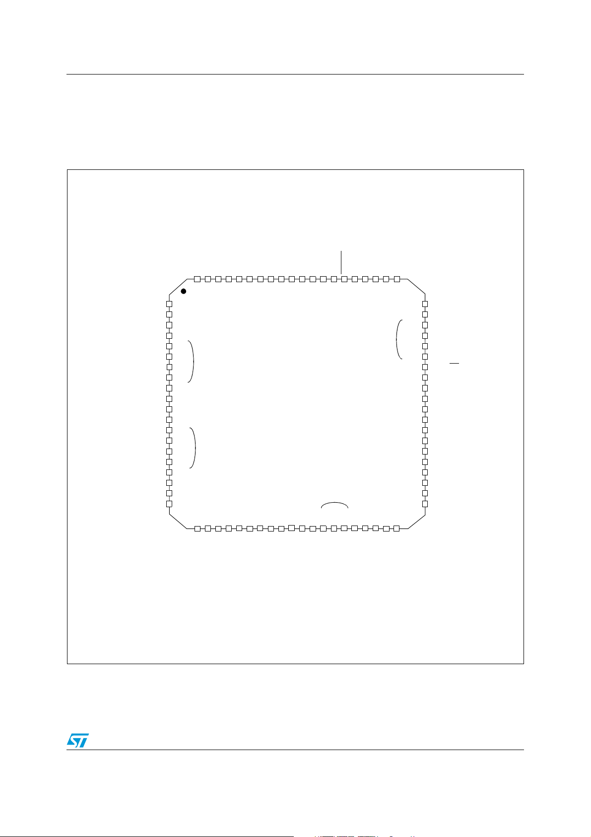
ST72521xx-Auto Package pinout and pin description
2
1
3
4
5
6
7
8
10
9
12
14
16
18
20
11
15
13
17
19
25
262827
30
32
34
36
38
29
33
31
35
37
39
57
58
56
55
54
53
52
51
49
50
47
45
43
41
48
44
46
42
60
59
61
62
63
64
666865
67
69
70
71
727473
75
76
77
78
79
80
PA 4 ( HS )
V
SS_1
V
DD_1
PA3 ( HS)
PC3 (HS) / ICAP1_B
PC2 (HS) / ICAP2_B
PC1 / OCMP1_B / AIN13
PC0 / OCMP2_B / AIN12
PA7 (HS) / SCLI
PA6 (HS) / SDAI
PA 5 ( HS )
PA 2
PA 1
PA 0
PC7 / SS / AIN15
PH2
PC5 / MOSI / AIN14
PWM0 / PB3
PG0
PG1
PG2
AIN3 / PD3
(HS) PE7
PWM3 / PB0
PWM2 / PB1
PWM1 / PB2
PG3
ARTCLK / (HS) PB4
ARTIC1 / PB5
ARTIC2 / PB6
PB7
AIN0 / PD0
AIN1 / PD1
AIN2 / PD2
(HS) PE4
(HS) PE5
(HS) PE6
V
DD3
V
SS3
MCO /AIN8 / PF0
BEEP / (HS) PF1
ICAP1_A / (HS) / PF6
AIN6 / PD6
AIN7 / PD7
V
AREF
V
SSA
(HS) PF2
OCMP2_A / AIN9 /PF3
OCMP1_A/AIN10 /PF4
40
EXTCLK_A / (HS) PF7
21
222423
PG6
PG7
AIN4/PD4
AIN5 / PD5
PE0 / TDO
V
SS
_2
TLI
EVD
RESET
V
PP
/ ICCSEL
PE3 / CANRX
PE2 / CANRX
PE1 / RDI
PH7
PH6
OSC1
OSC2
PC4 / MISO / ICCDATA
PH1
PH3
PC6 / SCK /ICCCLK
PH4
PH5
V
DD
_2
PG4
PG5
V
SS_0
V
DD_0
ICAP2_A/ AIN11 /PF5
PH0
(HS) 20mA high sink capability
eix associated external interrupt vector
ei1
ei3
ei2
ei0
2 Package pinout and pin description
2.1 Package pinout
Figure 2. 80-pin LQFP 14x14 package pinout
Doc ID 17660 Rev 1 21/276
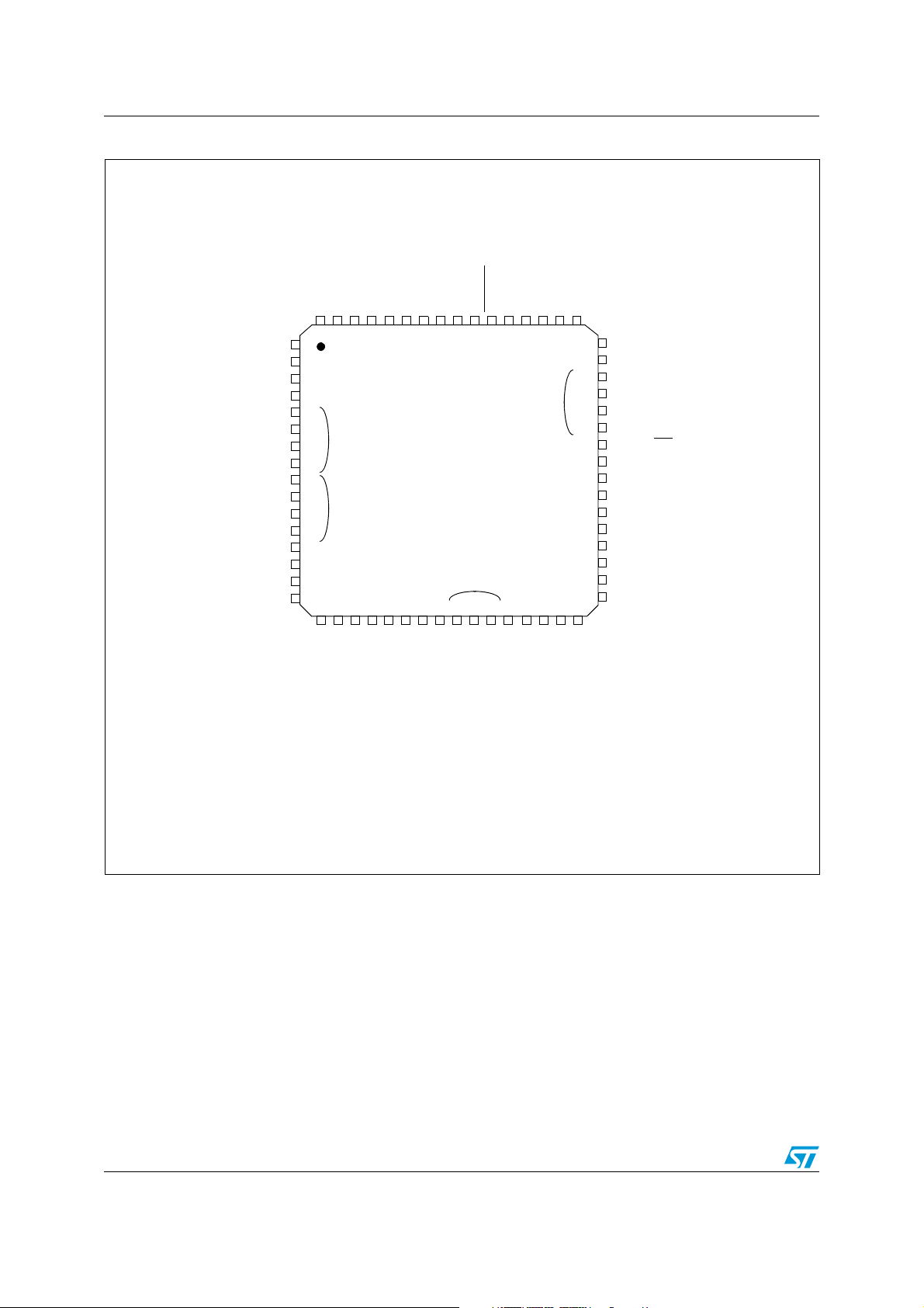
Package pinout and pin description ST72521xx-Auto
V
AREF
V
SSA
V
DD_3
V
SS_3
MCO / AIN8 / PF0
BEEP / (HS) PF1
(HS) PF2
OCMP2_A / AIN9 / PF3
OCMP1_A / AIN10 / PF4
ICAP2_A / AIN11 / PF5
ICAP1_A / (HS) PF6
EXTCLK_A / (HS) PF7
AIN4 / PD4
AIN5 / PD5
AIN6 / PD6
AIN7 / PD7
64 63 62 61 60 59 58 57 56 55 54 53 52 51 50 49
48
47
46
45
44
43
42
41
40
39
38
37
36
35
34
33
17 18 19 20 21 22 23 24 29 30 31 3225 26 27 28
1
2
3
4
5
6
7
8
9
10
11
12
13
14
15
16
ei2
ei3
ei0
ei1
PWM3 / PB0
PWM2 / PB1
PWM1 / PB2
PWM0 / PB3
ARTCLK / (HS) PB4
ARTIC1 / PB5
ARTIC2 / PB6
PB7
AIN0 / PD0
AIN1 / PD1
AIN2 / PD2
AIN3 / PD3
(HS) PE4
(HS) PE5
(HS) PE6
(HS) PE7
PA 1
PA 0
PC7 / SS
/ AIN15
PC6 / SCK / ICCCLK
PC5 / MOSI / AIN14
PC4 / MISO / ICCDATA
PC3 (HS) / ICAP1_B
PC2 (HS) / ICAP2_B
PC1 / OCMP1_B / AIN13
PC0 / OCMP2_B / AIN12
V
SS_0
V
DD_0
V
SS_1
V
DD_1
PA3 (HS )
PA 2
V
DD
_
2
OSC1
OSC2
V
SS
_
2
TLI
EVD
RESET
V
PP
/ ICCSEL
PA7 (HS) / SCLI
PA6 (HS) / SDAI
PA5 (HS)
PA4 (HS)
PE3 / CANRX
PE2 / CANTX
PE1 / RDI
PE0 / TDO
(HS) 20mA high sink capability
eix associated external interrupt vector
Figure 3. 64-pin LQFP 14x14 and 10x10 package pinout
For external pin connection guidelines, refer to Section 20: Electrical characteristics.
22/276 Doc ID 17660 Rev 1
ST72521xx-Auto Package pinout and pin description
2.2 Pin description
In the device pin description table, the RESET configuration of each pin is shown in bold.
This configuration is valid as long as the device is in reset state.
Refer to Section 9: I/O ports on page 73 for more details on the software configuration of the
I/O ports.
LQFP64
Pin
Name
Level Port
Typ e
Input
Output
float
Input Output
int
wpu
ana
OD
Main
function
(after
reset)
PP
Alternate function
Table 3. Device pin description
No.
LQFP80
1 1 PE4 (HS) I/O CTHS X XXXPort E4
2 2 PE5 (HS) I/O C
3 3 PE6 (HS) I/O C
4 4 PE7 (HS) I/O C
5 5 PB0/PWM3 I/O C
6 6 PB1/PWM2 I/O C
7 7 PB2/PWM1 I/O C
8 8 PB3/PWM0 I/O C
-
9
PG0 I/O T
(1)
-
10
11
12
PG1 I/O T
(1)
PG2 I/O T
(1)
PG3 I/O T
(1)
HS X XXXPort E5
T
HS X XXXPort E6
T
HS X XXXPort E7
T
T
T
T
T
T
T
T
T
X ei2 X X Port B0 PWM Output 3
X ei2 X X Port B1 PWM Output 2
X ei2 X X Port B2 PWM Output 1
X ei2 X X Port B3 PWM Output 0
X X X X Port G0
X X X X Port G1
X X X X Port G2
X X X X Port G3
13 9 PB4 (HS)/ARTCLK I/O CTHS X ei3 X X Port B4 PWM-ART External Clock
14 10 PB5/ARTIC1 I/O C
15 11 PB6/ARTIC2 I/O C
16 12 PB7 I/O C
17 13 PD0 /AIN0 I/O C
18 14 PD1/AIN1 I/O C
19 15 PD2/AIN2 I/O C
20 16 PD3/AIN3 I/O C
-
21
PG6 I/O T
(1)
T
T
T
T
T
T
T
T
X ei3 X X Port B5 PWM-ART Input Capture 1
X ei3 X X Port B6 PWM-ART Input Capture 2
X ei3 X X Port B7
X X X X X Port D0 ADC Analog Input 0
X X X X X Port D1 ADC Analog Input 1
X X X X X Port D2 ADC Analog Input 2
X X X X X Port D3 ADC Analog Input 3
X X X X Port G6
22
PG7 I/O T
(1)
T
X X X X Port G7
Doc ID 17660 Rev 1 23/276
Package pinout and pin description ST72521xx-Auto
Table 3. Device pin description (continued)
Pin
No.
Type
LQFP80
Name
LQFP64
23 17 PD4/AIN4 I/O C
24 18 PD5/AIN5 I/O C
25 19 PD6/AIN6 I/O C
26 20 PD7/AIN7 I/O C
27 21 V
28 22 V
29 23 V
30 24 V
-
31
(1)
(2)
AREF
(2)
SSA
(2)
DD_3
(2)
SS_3
PG4 I/O T
I Analog Reference Voltage for ADC
S Analog Ground Voltage
S Digital Main Supply Voltage
S Digital Ground Voltage
Level Port
Input Output
Input
Output
float
T
T
T
T
T
X X X X X Port D4 ADC Analog Input 4
X X X X X Port D5 ADC Analog Input 5
X X X X X Port D6 ADC Analog Input 6
X X X X X Port D7 ADC Analog Input 7
X X X X Port G4
int
wpu
ana
OD
Main
function
(after
reset)
PP
Alternate function
-
32
PG5 I/O T
(1)
33 25 PF0/MCO/AIN8 I/O C
34 26 PF1 (HS)/BEEP I/O C
35 27 PF2 (HS) I/O C
36 28 PF3/OCMP2_A/AIN9 I/O C
37 29 PF4/OCMP1_A/AIN10 I/O C
38 30 PF5/ICAP2_A/AIN11 I/O C
T
T
T
T
T
T
T
X X X X Port G5
X ei1 XXXPort F0
Main clock
out (f
CPU
)
ADC Analog
Input 8
HS X ei1 X X Port F1 Beep signal output
HS X ei1 X X Port F2
X X XXXPort F3
X X XXXPort F4
X X XXXPort F5
Timer A
Output
Compare 2
Timer A
Output
Compare 1
Timer A Input
Capture 2
ADC Analog
Input 9
ADC Analog
Input 10
ADC Analog
Input 11
39 31 PF6 (HS)/ICAP1_A I/O CTHS X X X X Port F6 Timer A Input Capture 1
40 32 PF7 (HS)/EXTCLK_A I/O CTHS X XXXPort F7
41 33 V
42 34 V
43 35 PC0/OCMP2_B/AIN12 I/O C
44 36 PC1/OCMP1_B/AIN13 I/O C
DD_0
SS_0
(2)
(2)
S Digital Main Supply Voltage
S Digital Ground Voltage
T
T
X X XXXPort C0
X X XXXPort C1
Timer A External Clock
Source
Timer B
Output
Compare 2
Timer B
Output
Compare 1
ADC Analog
Input 12
ADC Analog
Input 13
24/276 Doc ID 17660 Rev 1
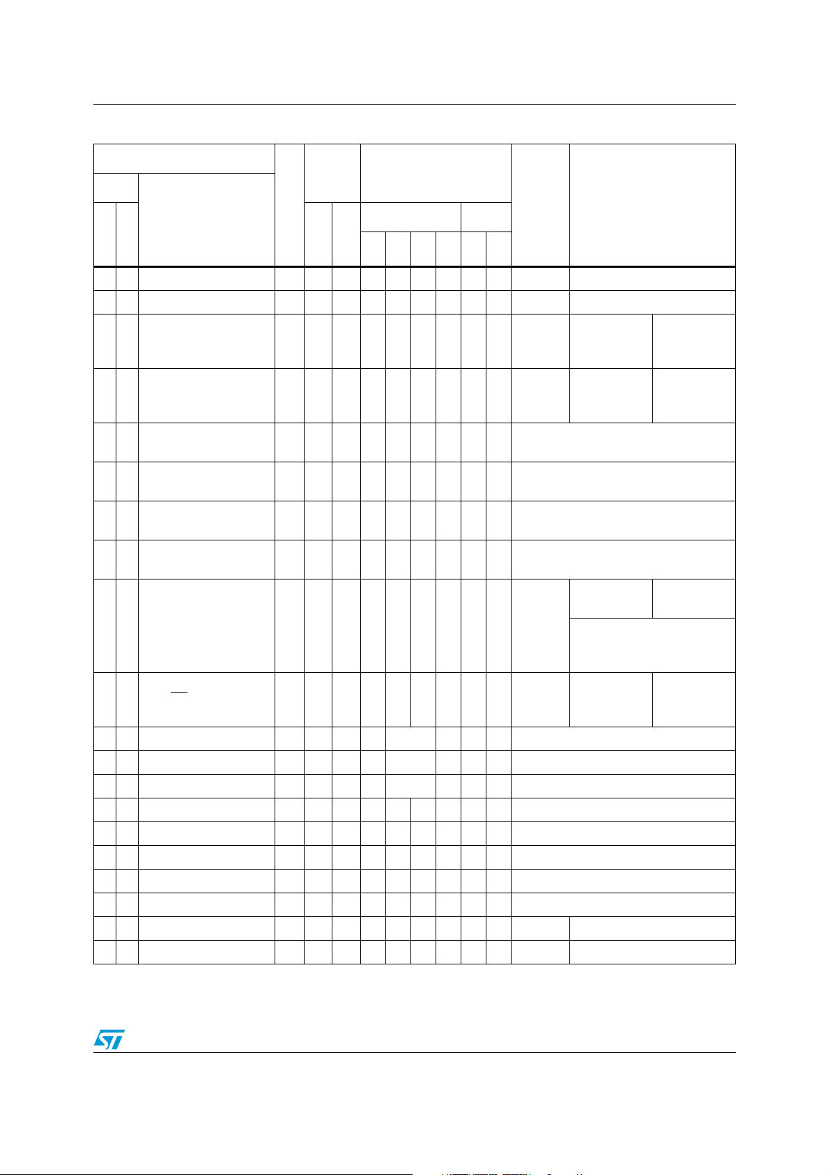
ST72521xx-Auto Package pinout and pin description
Table 3. Device pin description (continued)
Pin
No.
Type
LQFP80
Name
LQFP64
45 37 PC2 (HS)/ICAP2_B I/O C
46 38 PC3 (HS)/ICAP1_B I/O C
47 39 PC4/MISO/ICCDATA I/O C
Level Port
Input Output
Input
Output
float
HS X X X X Port C2 Timer B Input Capture 2
T
HS X X X X Port C3 Timer B Input Capture 1
T
T
X XXXPort C4
int
wpu
ana
OD
Main
function
(after
reset)
PP
Alternate function
SPI Master
In / Slave Out
Data
ICC Data
Input
48 40 PC5/MOSI/AIN14 I/O C
-
49
50
51
52
PH0 I/O T
(1)
PH1 I/O T
(1)
PH2 I/O T
(1)
PH3 I/O T
(1)
53 41 PC6/SCK/ICCCLK I/O C
54 42 PC7/SS
/AIN15 I/O C
55 43 PA0 I/O C
56 44 PA1 I/O C
57 45 PA2 I/O C
58 46 PA3 (HS) I/O C
59 47 V
60 48 V
DD_1
SS_1
(2)
(2)
S Digital Main Supply Voltage
S Digital Ground Voltage
61 49 PA4 (HS) I/O C
62 50 PA5 (HS) I/O C
63 51 PA6 (HS)/SDAI I/O C
64 52 PA7 (HS)/SCLI I/O C
SPI Master
T
X X XXXPort C5
Out / Slave In
Data
T
T
T
T
X XXXPort H0
X XXXPort H1
X XXXPort H2
X XXXPort H3
SPI Serial
Clock
T
X XXXPort C6
Caution: Negative current
injection not allowed on this
pin (Flash devices only)
SPI Slave
T
X X XXXPort C7
Select (active
low)
T
T
T
T
T
T
T
T
X ei0 X X Port A0
X ei0 X X Port A1
X ei0 X X Port A2
HS X ei0 X X Port A3
HS X XXXPort A4
HS X XXXPort A5
HS X TPort A6 I
HS X TPort A7 I
2
C Data
2
C Clock
ADC Analog
Input 14
ICC Clock
Output
ADC Analog
Input 15
Doc ID 17660 Rev 1 25/276
Package pinout and pin description ST72521xx-Auto
Table 3. Device pin description (continued)
Pin
Level Port
No.
LQFP80
LQFP64
Name
Type
Input
Output
Input Output
int
float
wpu
ana
OD
65 53 VPP/ ICCSEL I
66 54 RESET
I/O C
T
67 55 EVD I A External voltage detector
Main
function
(after
Alternate function
reset)
PP
Must be tied low. In Flash
programming mode, this pin acts as
the programming voltage input V
PP
See Section 20.9.2 on page 242 for
more details. High voltage must not be
applied to ROM devices.
Top priority non-maskable interrupt
..
68 56 TLI I C
-
69
70
71
72
73 57 V
74 58 OSC2
75 59 OSC1
76 60 V
PH4 I/O T
(1)
PH5 I/O T
(1)
PH6 I/O T
(1)
PH7 I/O T
(1)
(2)
SS_2
(3)
(3)
(2)
DD_2
77 61 PE0/TDO I/O C
78 62 PE1/RDI I/O C
79 63 PE2/CANTX I/O C
80 64 PE3/CANRX I/O C
1. On the chip, each I/O port may have up to 8 pads. Pads that are not bonded to external pins are in input pull-up
configuration after reset. The configuration of these pads must be kept at reset state to avoid added current consumption
2. It is mandatory to connect all available V
3. OSC1 and OSC2 pins connect a crystal/ceramic resonator or an external source to the on-chip oscillator; see Section 6.4:
Multi-oscillator (MO) on page 41 and Section 20.5: Clock and timing characteristics on page 228 for more details.
T
T
T
T
T
S Digital Ground Voltage
I/O Resonator oscillator inverter output
I
S Digital Main Supply Voltage
T
T
T
T
and V
DD
X X Top level interrupt input pin
X XXXPort H4
X XXXPort H5
X XXXPort H6
X XXXPort H7
External clock input or Resonator
oscillator inverter input
X X X X Port E0 SCI Transmit Data Out
X X X X Port E1 SCI Receive Data In
X Port E2 CAN Transmit Data Output
X X X X Port E3 CAN Receive Data Input
pins to the supply voltage and all VSS and V
AREF
pins to ground.
SSA
Legend / Abbreviations for Tabl e 3 :
Type: I = input
O = output
S = supply
Input level: A = dedicated analog input
26/276 Doc ID 17660 Rev 1

ST72521xx-Auto Package pinout and pin description
In/Output level: C = CMOS 0.3VDD/0.7V
DD
CT= CMOS 0.3VDD/0.7VDD with input trigger
Output level: HS = 20mA high sink (on N-buffer only)
Port and control configuration:
● Input: float = floating
wpu = weak pull-up
int = interrupt
(a)
ana = analog
● Output: OD = open-drain
(b)
PP = push-pull
a. In the interrupt input column, “eiX” defines the associated external interrupt vector. If the weak pull-up column
(wpu) is merged with the interrupt column (int), then the I/O configuration is pull-up interrupt input, otherwise
the configuration is floating interrupt input.
b. In the open-drain output column, “T” defines a true open-drain I/O (P-Buffer and protection diode to V
implemented). See Section 9: I/O ports on page 73 and Section 20.8: I/O port pin characteristics on page 236
for more details.
are not
DD
Doc ID 17660 Rev 1 27/276
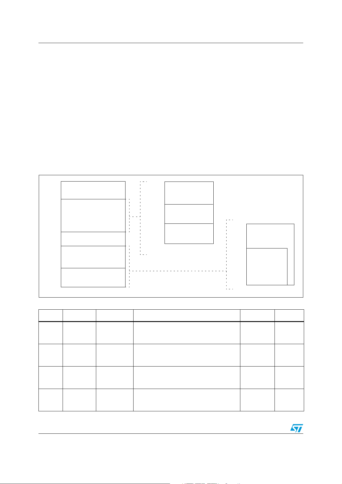
Register and memory map ST72521xx-Auto
0000h
RAM
Program Memory
(60K or 32K)
Interrupt & Reset Vectors
HW Registers
0080h
007Fh
0FFFh
(see Table 4)
1000h
FFDFh
FFE0h
FFFFh
(see Ta bl e 2 0 )
0880h
Reserved
087Fh
Short Addressing
RAM (zero page)
256 Bytes Stack
16-bit Addressing
RAM
0100h
01FFh
0080h
0200h
00FFh
or 087Fh
32 KBytes
8000h
60 KBytes
FFFFh
1000h
(2048 or 1024 Bytes)
or 067Fh
or 047Fh
3 Register and memory map
As shown in Figure 4, the MCU is capable of addressing 64 Kbytes of memories and I/O
registers.
The available memory locations consist of 128 bytes of register locations, up to 2 Kbytes of
RAM and up to 60 Kbytes of user program memory. The RAM space includes up to 256
bytes for the stack from 0100h to 01FFh.
The highest address bytes contain the user reset and interrupt vectors.
IMPORTANT: Memory locations marked as “Reserved” must never be accessed. Accessing
a reserved area can have unpredictable effects on the device.
Related documentation
Executing Code in ST7 RAM (AN 985)
Figure 4. Memory map
Table 4. Hardware register map
Address Block Register label Register name Reset status Remarks
0000h
0001h
Por t A
0002h
0003h
0004h
Por t B
0005h
0006h
0007h
0008h
0009h
000Ah
000Bh
Por t C
Por t D
28/276 Doc ID 17660 Rev 1
PA DR
PA DDR
PA OR
PBDR
PBDDR
PBOR
PCDR
PCDDR
PCOR
PDDR
PDDDR
PDOR
Port A Data Register
Port A Data Direction Register
Port A Option Register
Port B Data Register
Port B Data Direction Register
Port B Option Register
Port C Data Register
Port C Data Direction Register
Port C Option Register
Port D Data Register
Port D Data Direction Register
Port D Option Register
00h
00h
00h
00h
00h
00h
00h
00h
00h
00h
00h
00h
(1)
(1)
(1)
(1)
R/W
R/W
R/W
R/W
R/W
R/W
R/W
R/W
R/W
R/W
R/W
R/W
ST72521xx-Auto Register and memory map
Table 4. Hardware register map (continued)
Address Block Register label Register name Reset status Remarks
(1)
(1)
1)
1)
R/W
(2)
R/W
(2)
R/W
R/W
R/W
R/W
R/W
R/W
R/W
R/W
R/W
R/W
R/W
Read Only
Read Only
R/W
R/W
R/W
R/W
000Ch
000Dh
000Eh
000Fh
0010h
0011h
0012h
0013h
0014h
0015h
0016h
0017h
0018h
0019h
001Ah
001Bh
001Ch
001Dh
001Eh
001Fh
0020h
Por t E
Por t F
Por t G
Por t H
2
C
I
2)
2)
PEDR
PEDDR
PEOR
PFDR
PFDDR
PFOR
PGDR
PGDDR
PGOR
PHDR
PHDDR
PHOR
I2CCR
I2CSR1
I2CSR2
I2CCCR
I2COAR1
I2COAR2
I2CDR
Port E Data Register
Port E Data Direction Register
Port E Option Register
Port F Data Register
Port F Data Direction Register
Port F Option Register
Port G Data Register
Port G Data Direction Register
Port G Option Register
Port H Data Register
Port H Data Direction Register
Port H Option Register
2
C Control Register
I
2
C Status Register 1
I
I2C Status Register 2
2
C Clock Control Register
I
I2C Own Address Register 1
I2C Own Address Register2
2
C Data Register
I
Reserved Area (2 bytes)
00h
00h
00h
00h
00h
00h
00h
00h
00h
00h
00h
00h
00h
00h
00h
00h
00h
00h
00h
0021h
0022h
0023h
0024h
0025h
0026h
0027h
SPI
ITC
SPIDR
SPICR
SPICSR
ISPR0
ISPR1
ISPR2
ISPR3
SPI Data I/O Register
SPI Control Register
SPI Control/Status Register
Interrupt Software Priority Register 0
Interrupt Software Priority Register 1
Interrupt Software Priority Register 2
Interrupt Software Priority Register 3
xxh
0xh
00h
FFh
FFh
FFh
FFh
R/W
R/W
R/W
R/W
R/W
R/W
R/W
0028h EICR External Interrupt Control Register 00h R/W
0029h FLASH FCSR Flash Control/Status Register 00h R/W
002Ah WATCHDOG WDGCR Watchdog Control Register 7Fh R/W
002Bh SICSR System Integrity Control/Status Register 000x 000x b R/W
002Ch
002Dh
MCC
MCCSR
MCCBCR
Main Clock Control / Status Register
Main Clock Controller: Beep Control Register
00h
00h
R/W
R/W
002Eh
to
Reserved Area (3 bytes)
0030h
Doc ID 17660 Rev 1 29/276

Register and memory map ST72521xx-Auto
Table 4. Hardware register map (continued)
Address Block Register label Register name Reset status Remarks
0031h
0032h
0033h
0034h
0035h
0036h
0037h
0038h
0039h
003Ah
003Bh
003Ch
003Dh
003Eh
003Fh
0040h Reserved Area (1 byte)
0041h
0042h
0043h
0044h
0045h
0046h
0047h
0048h
0049h
004Ah
004Bh
004Ch
004Dh
004Eh
004Fh
0050h
0051h
0052h
0053h
0054h
0055h
0056h
0057h
TIMER A
TIMER B
SCI
TACR2
TACR1
TA CS R
TA I C1 H R
TAIC1LR
TA OC 1 H R
TA OC 1 L R
TACHR
TA CL R
TA AC H R
TA AC L R
TA I C2 H R
TAIC2LR
TA OC 2 H R
TA OC 2 L R
TBCR2
TBCR1
TBCSR
TBIC1HR
TBIC1LR
TBOC1HR
TBOC1LR
TBCHR
TBCLR
TBACHR
TBACLR
TBIC2HR
TBIC2LR
TBOC2HR
TBOC2LR
SCISR
SCIDR
SCIBRR
SCICR1
SCICR2
SCIERPR
SCIETPR
Timer A Control Register 2
Timer A Control Register 1
Timer A Control/Status Register
Timer A Input Capture 1 High Register
Timer A Input Capture 1 Low Register
Timer A Output Compare 1 High Register
Timer A Output Compare 1 Low Register
Timer A Counter High Register
Timer A Counter Low Register
Timer A Alternate Counter High Register
Timer A Alternate Counter Low Register
Timer A Input Capture 2 High Register
Timer A Input Capture 2 Low Register
Timer A Output Compare 2 High Register
Timer A Output Compare 2 Low Register
Timer B Control Register 2
Timer B Control Register 1
Timer B Control/Status Register
Timer B Input Capture 1 High Register
Timer B Input Capture 1 Low Register
Timer B Output Compare 1 High Register
Timer B Output Compare 1 Low Register
Timer B Counter High Register
Timer B Counter Low Register
Timer B Alternate Counter High Register
Timer B Alternate Counter Low Register
Timer B Input Capture 2 High Register
Timer B Input Capture 2 Low Register
Timer B Output Compare 2 High Register
Timer B Output Compare 2 Low Register
SCI Status Register
SCI Data Register
SCI Baud Rate Register
SCI Control Register 1
SCI Control Register 2
SCI Extended Receive Prescaler Register
Reserved area
SCI Extended Transmit Prescaler Register
00h
00h
xxxx x0xx b
xxh
xxh
80h
00h
FFh
FCh
FFh
FCh
xxh
xxh
80h
00h
00h
00h
xxxx x0xx b
xxh
xxh
80h
00h
FFh
FCh
FFh
FCh
xxh
xxh
80h
00h
C0h
xxh
00h
x000 0000b
00h
00h
---
00h
R/W
R/W
R/W
Read Only
Read Only
R/W
R/W
Read Only
Read Only
Read Only
Read Only
Read Only
Read Only
R/W
R/W
R/W
R/W
R/W
Read Only
Read Only
R/W
R/W
Read Only
Read Only
Read Only
Read Only
Read Only
Read Only
R/W
R/W
Read Only
R/W
R/W
R/W
R/W
R/W
R/W
0058h
0059h
005Ah
005Bh
005Ch
005Dh
005Eh
005Fh
0060h
to
006Fh
30/276 Doc ID 17660 Rev 1
CAN
CANISR
CANICR
CANCSR
CANBRPR
CANBTR
CANPSR
CAN Interrupt Status Register
CAN Interrupt Control Register
CAN Control / Status Register
CAN Baud Rate Prescaler Register
CAN Bit Timing Register
CAN Page Selection Register
First address
to
Last address of CAN page x
Reserved Area (2 Bytes)
00h
00h
00h
00h
23h
00h
--
R/W
R/W
R/W
R/W
R/W
R/W
See CAN
Descriptio
n
 Loading...