

Page 1

AN5595
Application note
SPC58xEx/SPC58xGx multimedia card via SPI interface
Introduction
The multimedia card is a universal data storage and communication media device. It is designed to support a wide range of
applications, in particular more recently on automotive products.
This AN5595 describes about the SPI mode to control the MMC/SD cards. The software application has been developed by
using the SPC58xEx/SPC58xGx microcontroller and its software development is based on top of SPC5-STUDIO tool available
at the following link: https://www.st.com/en/development-tools/spc5-studio.html.
The SPI mode is an alternative operating mode that is defined to use the MMC/SD cards on microcontrollers without a native
host interface. The MMC/SD can be used on a microcontroller via a generic SPI interface or some GPIO ports. Therefore,
the SPI mode is suitable for low cost embedded applications. This mode can be accepted on platforms where no specific
performances are required and where some limitations of the MMC/SD protocol via SPI mode do not impact on system
requirements.
AN5595 - Rev 1 - January 2021
For further information contact your local STMicroelectronics sales office.
www.st.com
Page 2

1 MMC basic concepts
The multimedia card transfers data via a configurable number of data bus signals:
• CLK: the frequency may vary according to the card speed
• CMD: is a bidirectional command channel used for card initialization and transfer of commands
• DAT0-DAT7: these are bidirectional data channels; the multimedia card includes internal pull-ups for all data
lines
Useful terms and definitions while talking about the multimedia card:
• Block: number of bytes, basic data transfer unit
• CID: card identification number register
• CLK: clock signal
• CMD: command line or multimedia card bus command (if extended CMDXX)
• CSD: card specific data register
• OCR: operation conditions register
• CD: card detection
• W/P: write protection
AN5595
MMC basic concepts
AN5595 - Rev 1
page 2/25
Page 3

2 Card registers
Within the card interface six register classes are defined:
• The operation conditions register (OCR) stores the VDD voltage profile
• The card identification (CID): manufacturer ID, product name, revision
• The card-specific data (CSD) register provides information on how to access the card contents. The CSD
defines the data format, error correction type, maximum data access time, data transfer speed, whether the
DSR register can be used
• The extended CSD register defines the card properties and selected modes
• The relative card address (RCA) register carries the card address assigned by the host during the card
identification
• The driver stage register (DSR) optionally used to improve the bus performance for extended operating
conditions
AN5595
Card registers
AN5595 - Rev 1
page 3/25
Page 4

3 MMC/SD SPI mode introduction
The SPI mode has been removed from new specifications, but it can be found in previous JEDEC standard
No. JESD84-B41.
The communication protocol of the SPI mode is rather simple compared to its native operating mode.
The MMC/SDC can be attached to the microcontroller via a generic SPI interface as shown below:
Figure 1. SPI bus connection
AN5595
MMC/SD SPI mode introduction
While the multimedia card is based on command and data bit streams which are initiated by a start bit and
terminated by a stop bit, the SPI channel is byte oriented. Each command or data block consists of 8-bit bytes
and his octet aligned on the CS signal. Like the multimedia card protocol, the SPI messages consist of command,
response, and data-block tokens.
The response behavior in the SPI mode differs from the multimedia card mode in the following three aspects:
• The selected card always responds to the command
• Additional (8-, 16- and 40-bit) response structures are used
• When the card encounters a data retrieval problem, it will respond with an error response rather than a
time-out
AN5595 - Rev 1
page 4/25
Page 5

4 DSPI overview
The SPC58x microcontroller embeds the deserial serial peripheral interface (DSPI) module. This provides a
synchronous serial bus for communication between an MCU and an external peripheral device.
The DSPI supports the MCU pin count reduction through serialization and deserialization of the MCU internal
signals transmitted over the SPI serial link. The DSPI supports different modes including the SPI. All the
necessary information about the DSPI can be found inside the microcontroller’s reference manual.
AN5595
DSPI overview
AN5595 - Rev 1
page 5/25
Page 6

5 SPI signals
The SPI mode is compliant with the serial peripheral interface (SPI) specification: its bus architecture includes the
following signals:
• CS: host to card chip select signal
• CLK: host to card clock signal
• MOSI: (master out slave in) host to card single bit data signal
• MISO: (master in slave out) card to host single bit data signal
The SPI mode is implemented to access the MMC/SD media card so:
• Every transaction by asserting the CS signal low
• Commands and tx data are sent to the media card on the MOSI line
• Command response and RX data are received from the media card on the MISO line
• The CLK signal is used to synchronize the data transfer on the bus
AN5595
SPI signals
Figure 2. Card signals
AN5595 - Rev 1
page 6/25
Page 7

Figure 3. Signal comparisons (MMC versus SPI) from standard
AN5595
SPI signals
AN5595 - Rev 1
page 7/25
Page 8

6 MMC/SD SPI protocol
6.1 Initialization procedure
After power on reset, MMC/SDC enters are native operating modes.
The card will enter SPI mode if the CS signal is low during the reception of the reset command (CMD0) and it will
respond with SPI mode R1 response.
The only way to return to the multimedia card mode is by a power cycle (turn the power off and on).
Since CMD0 has no arguments, the content of all the fields plus the CRC (not calculated by the card) field are
constant.
Reset command:0x40, 0x0, 0x0, 0x0, 0x0, 0x95
In idle state, the card accepts only CMD0, CMD1, ACMD41, CMD58 and CMD59.
Note that all cards work at supply voltage range of 2.7 to 3.6 V at least, so that the host controller doesn't need to
check the OCR if the supply voltage is in this range.
In SPI mode the CMD1 has no operands and does not return the contents of the OCR register. Instead, the host
may use CMD58 (only in SPI mode) to read the OCR.
Figure 4. Example of initialization flow chart
AN5595
MMC/SD SPI protocol
AN5595 - Rev 1
page 8/25
Page 9

6.2 Clock control
The SPI bus clock signal can be used to put the card into energy saving mode or to control the data flow.
There are a few restrictions the SPI host must follow:
• The frequency can be changed at any time
• After the last SPI bus transaction, the host is required to provide 8 clock cycles for the card to complete the
operation before shutting down the clock.
• A command / response sequence, 8 clocks after the card response end bit. The CS signal can be asserted
or de-asserted during these 8 clocks.
• A read data transaction, 8 clocks after the end bit of the last data block.
• A write data transaction, 8 clocks after the CRC status token.
• The host can shut down the clock of a “busy” card
6.3 CMD0 and R1 response
Host controller sends the CMD0 reset command:
0x40, 0x0, 0x0, 0x0, 0x0, 0x95
AN5595
Clock control
Figure 5. CMD0 reset command
Card R1 response: 0x1 (IDLE_STATE)
Figure 6. R1 response
AN5595 - Rev 1
page 9/25
Page 10

6.4 Data transfer - Data read
The SPI mode supports single and multiple blocks read operations.
6.4.1 SPI single block read operation
When a READ_SINGLE_BLOCK (CMD17) is accepted, a read operation is initiated, and the read data block is
sent. After a valid data token, the host controller receives the data field and CRC.
CID/CSD registers: in SPI mode is a simple read-block transaction.
Figure 7. SPI single block read operation
AN5595
Data transfer - Data read
6.4.2 SPI multiple blocks read operation
The CMD18 is to read multiple blocks in sequence. To terminate the transaction, send a CMD12 to the card.
Figure 8. SPI multi block read operation
6.4.3 SPI read operation - data error
Multiple blocks read operation can be terminated the same way, the error token replacing a data block anywhere
in the sequence. After receiving the CMD12 the card replies with ADDRESS_MISALIGN bit set.
Figure 9. SPI read operation—data error
AN5595 - Rev 1
page 10/25
Page 11
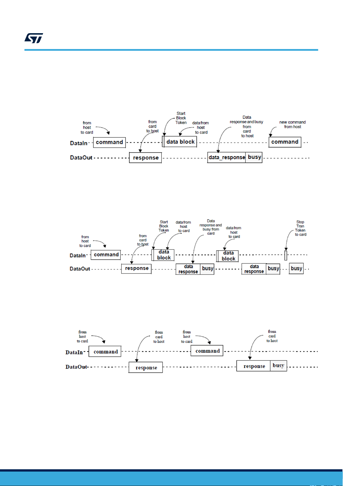
6.4.4 SPI single block write operation
The SINGLE_BLOCK_WRITE writes a block to the card. After a CMD24 is accepted, the host controller sends
a data packet to the card. Often the block size is fixed to 512 bytes. The CS signal must be kept low during a
transaction. The data response trails a busy flag and host controller must wait until the card goes ready.
Figure 10. SPI single block write operation
6.4.5 SPI multiple blocks write operation
After a CMD25 is accepted, the host controller sends one or more data packets to the card. The write operation
continues until terminated with a STOP_TOKEN. The number of block to write can be pre-defined by CMD23.
AN5595
Data transfer - Data read
6.4.6 SPI erase operation
The erase and write protect management procedures in the SPI mode are identical to those of the multimedia
card mode.
Figure 11. SPI multi block write operation
Figure 12. SPI erase operation
AN5595 - Rev 1
page 11/25
Page 12

7 Hardware setup
The Figure 13 shows the SPC58G discovery board connected to the TJCTM24028-SPI module. This is a
commercial module that provides both a display (not used in this demo application) and an SD slot that can
be programmed by an SPI interface.
AN5595
Hardware setup
Figure 13. Board connection
Note: the Figure 13 also shows an analyzer hardware plugged on the signals, this has been used for analyzing the SPI
protocol and look at the commands and SD card response.
AN5595 - Rev 1
page 12/25
Page 13

Figure 14. Wiring details
AN5595
Hardware setup
AN5595 - Rev 1
page 13/25
Page 14

AN5595
DSPI1 signal configuration
8 DSPI1 signal configuration
DSPI 1 has been used with the following signal configuration. For details about the SIUL2 refer to the
microcontroller’s reference manual.
Table 1. DSPI1 signal pins configuration
U301 pin SPI signals GPIO Direction SIUL2
10 T_SPI_CLK PD[6] OUT MSCR_54 (SSS 0x10)
11 T_SPI_CS PA[4] IN/OUT
12 T_SPI_SIN PF[13] IN MSCR_883 (SSS 0x111)
13 T_SPI_OUT PD[7] OUT MSCR_55 (SSS 0x011)
Note: the SIUL2 programming is detailed inside the MCU’s reference manual, SPC5-STUDIO provides a graphical
interface to configure the MCU signals too.
MSCR_4 (SSS 0x1)
MSCR_885 (SSS 0x100)
AN5595 - Rev 1
page 14/25
Page 15
9 Application
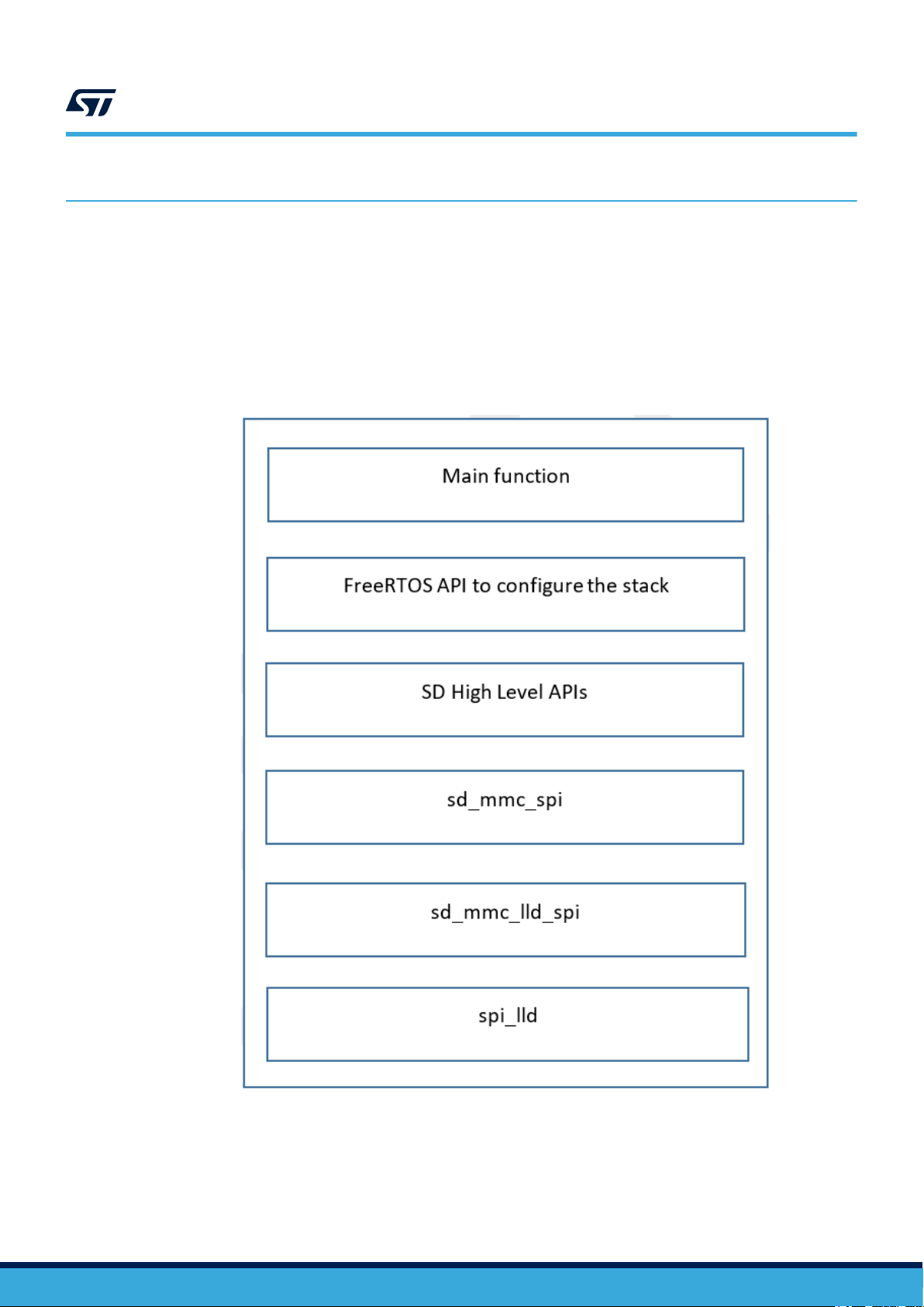
The following diagram in the Figure 15 aims at showing the basic application flow.
The software is based on FreeRTOS provided by the SPC5-STUDIO tool.
The main configures the microcontroller by using the API set provided by the SPC5-STUDIO tool. User can point
to the related SPC5-STUDIO documentation to become familiar with that.
As soon as the platform is configured (clock, signals, interrupts) the main function invokes the low-level APIs
designed to configure the SD card.
To dialog with the SD card the SPI low-level driver (available in SPC5-STUDIO) is configured since the beginning.
AN5595
Application
Figure 15. Application flow diagram
AN5595 - Rev 1
Optionally the FreeRTOS can use a file system to manage the SD card or the application can perform raw access
to it.
page 15/25
Page 16

9.1 Code example
This chapter will focus on the low-level part of the driver.
This is mainly composed by the sd_mmc_spi, sd_mmc_lld_spi and sp_lld driver components.
Due to the complexity of the code design, this document just reports some part of the software that can inspire the
user on developing his/her own one.
The sd_mmc.c file exposes the functions to manage the card, so these can be invoked by the upper layer stack
(e.g. operating file system support).
This is an example of the function used to check if the external card device can be initialized.
{
// Initialization of the card in SPI mode
if (sd_mmc_spi_card_init(sd_mmc_card)) {
sd_mmc_card->state = SD_MMC_CARD_STATE_READY;
SD_PRINT_DEBUG("MMC/SD card ready\n");
return SD_MMC_INIT_ONGOING;
}
SD_PRINT_DEBUG("MMC/SD card initialization failed\n");
sd_mmc_card->state = SD_MMC_CARD_STATE_UNUSABLE;
return SD_MMC_ERR_UNUSABLE;
}
AN5595
Code example
Note: the SD_PRINT_DEBUG is used to dump the message through the UART console.
The code below implements the read and write operations:
int sd_mmc_data_write (int aSecNr, const unsigned char *apBuf, int aSecCount, uint8_t type,
uint8_t wp)
{
uint8_t rc;
rc = sd_mmc_init_write_blocks(aSecNr, aSecCount, type, wp);
if (rc == SD_MMC_OK) {
rc = sd_mmc_start_write_blocks(apBuf, aSecCount);
if (rc == SD_MMC_OK) {
rc = sd_mmc_wait_end_of_write_blocks();
}
} else {
SD_PRINT_DEBUG ("sd_mmc_data_write(%lu) returns %d\n", aSecNr, rc);
}
rc = sd_mmc_check_status();
if (rc != SD_MMC_OK) {
SD_PRINT_DEBUG ("Warn: mmc_check_status %d\n", rc);
}
return rc == SD_MMC_OK;
}
int sd_mmc_data_read (int aSecNr, unsigned char *apBuf, int aSecCount, uint8_t type)
{
uint8_t rc;
rc = sd_mmc_init_read_blocks(aSecNr, aSecCount, type);
if (rc == SD_MMC_OK) {
rc = sd_mmc_start_read_blocks(apBuf, aSecCount);
if (rc == SD_MMC_OK) {
rc = sd_mmc_wait_end_of_read_blocks();
}
} else {
SD_PRINT_DEBUG ("sd_mmc_data_read(%lu) returns %d\n", aSecNr, rc);
}
return rc == SD_MMC_OK;
}
AN5595 - Rev 1
The sd_mmc_spi implements the SPI protocol and all the commands necessary to control MMC and SD cards.
For example, the card initialization is done by invoking the following function.
page 16/25
Page 17

bool sd_mmc_spi_card_init(struct sd_mmc_card_t *card)
{
uint8_t v2 = 0;
sd_mmc_card = card;
sd_mmc_card->type = CARD_TYPE_SD;
sd_mmc_card->version = CARD_VER_UNKNOWN;
sd_mmc_card->rca = 0;
// CMD0 - Reset all cards to idle state.
if (!spi_dvr_send_cmd(SDMMC_SPI_CMD0_GO_IDLE_STATE, 0)) {
return false;
}
SD_PRINT_DEBUG("%s: card reset to IDLE: done\n", __func__);
if (!sd_cmd8(&v2)) {
return false;
}
// Configure according the card type.
if (sd_mmc_card->type & CARD_TYPE_SD) {
// Try to get the SD card's operating condition
if (!sd_spi_op_cond(v2)) {
// It is not a SD card
SD_PRINT_DEBUG("No SD card, try to init MMC device...\n");
sd_mmc_card->type = CARD_TYPE_MMC;
return sd_mmc_spi_init_protocol();
}
if (!spi_dvr_send_cmd(SDMMC_SPI_CMD59_CRC_ON_OFF, 0)) {
return false;
}
}
// SD MEMORY
if (sd_mmc_card->type & CARD_TYPE_SD) {
// Get the Card-Specific Data
if (!sd_mmc_cmd9_spi()) {
return false;
}
sd_decode_csd();
// Read the SCR to get card version
if (!sd_acmd51()) {
return false;
}
}
if ((sd_mmc_card->type & CARD_TYPE_SDIO)) {
SD_PRINT_DEBUG("ERROR: Do not support SDIO device\n");
return false;
}
// SD MEMORY not HC, Set default block size
if ((sd_mmc_card->type & CARD_TYPE_SD) &&
(0 == (sd_mmc_card->type & CARD_TYPE_HC))) {
if (!spi_dvr_send_cmd(SDMMC_CMD16_SET_BLOCKLEN, SD_MMC_BLOCK_SIZE))
{
return false;
}
}
// Check communication
if (sd_mmc_card->type & CARD_TYPE_SD) {
if (!sd_mmc_cmd13()) {
return false;
}
}
// Reinitialize the slot with the new speed
return true;
}
AN5595
Code example
AN5595 - Rev 1
In the end, the sd_mmc_lld_spi calls the SPI low-level driver (sd_lld) to implement each command.
According to the driver included inside SPC5-STUDIO when this application has been developed, the following
APIs are used to send and receive over the SPI bus.
page 17/25
Page 18

static inline void spi_lld_send_wrap(size_t n, const void *buf)
{
spi_lld_start(spip, spi_config);
spi_lld_send(spip, n, buf);
spi_lld_stop(spip);
}
static inline void spi_lld_rx_wrap(size_t n, void *buf)
{
spi_lld_start(spip, spi_config);
spi_lld_receive(spip, n, buf);
spi_lld_stop(spip);
}
The following function is an example of the low-level function to read a block:
bool spi_dvr_start_read_blocks(void *dest, uint16_t nb_block)
{
uint32_t pos;
spi_dvr_err = SD_MMC_SPI_NO_ERR;
pos = 0;
while (nb_block--) {
configASSERT(spi_dvr_nb_block >
(spi_dvr_transfert_pos / spi_dvr_block_size));
if (!spi_dvr_start_read_block()) {
return false;
}
// Read block
spi_lld_rx_wrap(spi_dvr_block_size, &((uint8_t*)dest)[pos]);
pos += spi_dvr_block_size;
spi_dvr_transfert_pos += spi_dvr_block_size;
spi_dvr_stop_read_block();
}
return true;
}
AN5595
Code example
AN5595 - Rev 1
page 18/25
Page 19

9.2 Application output
The Figure 16 shows a part of the output from the serial console where the SD card is initialized and the file
system is recognized.
AN5595
Application output
Figure 16. Application output
AN5595 - Rev 1
Without the card plugged on, the following message is dumped:
Figure 17. Output with no card
page 19/25
Page 20

10 Conclusions
The main purpose of this document is to present a low-cost solution to support, on top of the SPC58
microcontroller family, the SD and MMC card on-board. The application is focused on the feasibility of this kind of
support and it has been demonstrated that external SD card can be configured and used by adopting the DSPI
controller.
The application shows how to setup the hardware, introduces the SPI protocol for MMC/SD card and shows some
basic APIs to manage the card.
Having an extra and large storage device, like MMC or SD cards, application can take the advantage to store files
for FOTA or other information (debug or diagnostic details). So, this can cover some ad-hoc requirements and
needs.
The application could be ported on other microcontrollers in this family, the software has been tested on the
SPC58xEx/SPC58xGx microcontroller. Minor changes or re-adaptation could be necessary to have the code on
top of the latest SPC5-STUDIO tool.
Due to the relationship with the card and software implementation, no performances have been measured in this
application as well as no test on critical conditions.
AN5595
Conclusions
AN5595 - Rev 1
page 20/25
Page 21

Revision history
AN5595
Table 2. Document revision history
Date Version Changes
19-Jan-2021 1 Initial release.
AN5595 - Rev 1
page 21/25
Page 22

AN5595
Contents
Contents
1 MMC basic concepts...............................................................2
2 Card registers .....................................................................3
3 MMC/SD SPI mode introduction....................................................4
4 DSPI overview .....................................................................5
5 SPI signals ........................................................................6
6 MMC/SD SPI protocol ..............................................................8
6.1 Initialization procedure ..........................................................8
6.2 Clock control ..................................................................9
6.3 CMD0 and R1 response.........................................................9
6.4 Data transfer - Data read .......................................................10
6.4.1 SPI single block read operation.............................................10
6.4.2 SPI multiple blocks read operation ..........................................10
6.4.3 SPI read operation - data error .............................................10
6.4.4 SPI single block write operation ............................................11
6.4.5 SPI multiple blocks write operation .......................................... 11
6.4.6 SPI erase operation .....................................................11
7 Hardware setup...................................................................12
8 DSPI1 signal configuration........................................................14
9 Application .......................................................................15
9.1 Code example ................................................................16
9.2 Application output .............................................................19
10 Conclusions ......................................................................20
Revision history .......................................................................21
AN5595 - Rev 1
page 22/25
Page 23

AN5595
List of tables
List of tables
Table 1. DSPI1 signal pins configuration ......................................................... 14
Table 2. Document revision history ............................................................. 21
AN5595 - Rev 1
page 23/25
Page 24

AN5595
List of figures
List of figures
Figure 1. SPI bus connection .................................................................4
Figure 2. Card signals......................................................................6
Figure 3. Signal comparisons (MMC versus SPI) from standard .........................................7
Figure 4. Example of initialization flow chart.......................................................8
Figure 5. CMD0 reset command...............................................................9
Figure 6. R1 response .....................................................................9
Figure 7. SPI single block read operation........................................................ 10
Figure 8. SPI multi block read operation ........................................................ 10
Figure 9. SPI read operation—data error ........................................................ 10
Figure 10. SPI single block write operation ....................................................... 11
Figure 11. SPI multi block write operation ........................................................ 11
Figure 12. SPI erase operation ............................................................... 11
Figure 13. Board connection ................................................................. 12
Figure 14. Wiring details ....................................................................13
Figure 15. Application flow diagram ............................................................15
Figure 16. Application output ................................................................. 19
Figure 17. Output with no card................................................................ 19
AN5595 - Rev 1
page 24/25
Page 25

AN5595
IMPORTANT NOTICE – PLEASE READ CAREFULLY
STMicroelectronics NV and its subsidiaries (“ST”) reserve the right to make changes, corrections, enhancements, modifications, and improvements to ST
products and/or to this document at any time without notice. Purchasers should obtain the latest relevant information on ST products before placing orders. ST
products are sold pursuant to ST’s terms and conditions of sale in place at the time of order acknowledgement.
Purchasers are solely responsible for the choice, selection, and use of ST products and ST assumes no liability for application assistance or the design of
Purchasers’ products.
No license, express or implied, to any intellectual property right is granted by ST herein.
Resale of ST products with provisions different from the information set forth herein shall void any warranty granted by ST for such product.
ST and the ST logo are trademarks of ST. For additional information about ST trademarks, please refer to www.st.com/trademarks. All other product or service
names are the property of their respective owners.
Information in this document supersedes and replaces information previously supplied in any prior versions of this document.
© 2021 STMicroelectronics – All rights reserved
AN5595 - Rev 1
page 25/25
 Loading...