

Page 1
SPC56EL60L3
SPC56EL60L5
32-bit Power Architecture® microcontroller for automotive
SIL3/ASILD chassis and safety applications
Features
■ High-performance e200z4d dual core
– 32-bit Power Architecture
– Core frequency as high as 120 MHz
– Dual issue five-stage pipeline core
– Variable Length Encoding (VLE)
– Memory Management Unit (MMU)
– 4 KB instruction cache with error detection
code
– Signal processing engine (SPE)
■ Memory available
– 1 MB Flash memory with ECC
– 128 KB on-chip SRAM with ECC
– Built-in RWW capabilities for EEPROM
emulation
■ SIL3/ASILD innovative safety concept:
LockStep mode and Fail-safe protection
– Sphere of replication (SoR) for key
components (such as CPU core, eDMA,
crossbar switch)
– Fault collection and control unit (FCCU)
– Redundancy control and checker unit
(RCCU) on outputs of the SoR connected
to FCCU
– Boot-time Built-In Self-Test for Memory
(MBIST) and Logic (LBIST) triggered by
hardware
– Boot-time Built-In Self-Test for ADC and
Flash memory triggered by software
– Replicated safety enhanced watchdog
– Replicated junction temperature sensor
– Non-maskable interrupt (NMI)
– 16-region memory protection unit (MPU)
– Clock monitoring units (CMU)
– Power management unit (PMU)
– Cyclic redundancy check (CRC) unit
®
technology CPU
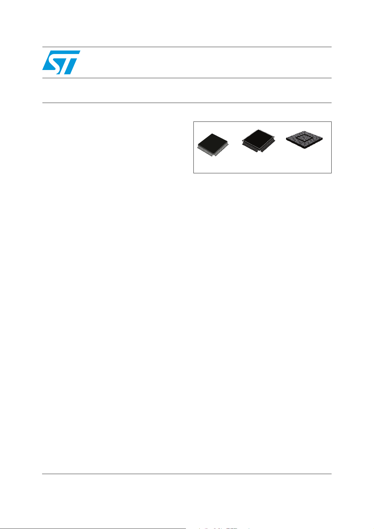
LQFP100
1. For development purpose only.
■ Decoupled Parallel mode for high-performance
LQFP144
20 x 20 mm
LBGA257
14 x 14 mm
(1)
use of replicated cores
■ Nexus Class 3+ interface
■ Interrupts
– Replicated 16-priority controller
– Replicated 16-channel eDMA controller
■ GPIOs individually programmable as input,
output or special function
■ Three 6-channel general-purpose eTimer units
■ 2 FlexPWM units: four 16-bit channels per
module
■ Communications interfaces
– 2 LINFlexD channels
– 3 DSPI channels with automatic chip select
generation
– 2 FlexCAN interfaces (2.0B Active) with 32
message objects
– FlexRay module (V 2.1 Rev. A) with 2
channels, 64 message buffers and data
rates up to 10 Mbit/s
■ Two 12-bit analog-to-digital converters (ADCs)
– 16 input channels
– Programmable cross triggering unit (CTU)
to synchronize ADCs conversion with timer
and PWM
■ Sine wave generator (D/A with low pass filter)
■ On-chip CAN/UART bootstrap loader
■ Single 3.0 V to 3.6 V voltage supply
■ Ambient temperature range –40 °C to 125 °C
■ Junction temperature range –40 °C to 150 °C
April 2011 Doc ID 15461 Rev 5 1/38
www.st.com
1
Page 2

SPC56EL60L3, SPC56EL60L5 Contents
Contents
1 Introduction . . . . . . . . . . . . . . . . . . . . . . . . . . . . . . . . . . . . . . . . . . . . . . . . 6
2 Features . . . . . . . . . . . . . . . . . . . . . . . . . . . . . . . . . . . . . . . . . . . . . . . . . . . 7
2.1 Device comparison . . . . . . . . . . . . . . . . . . . . . . . . . . . . . . . . . . . . . . . . . . . 7
2.2 Block diagram . . . . . . . . . . . . . . . . . . . . . . . . . . . . . . . . . . . . . . . . . . . . . . . 9
2.3 Operating parameters . . . . . . . . . . . . . . . . . . . . . . . . . . . . . . . . . . . . . . . 10
2.4 Modes of operation . . . . . . . . . . . . . . . . . . . . . . . . . . . . . . . . . . . . . . . . . . 11
2.4.1 Lock Step Mode (LSM) . . . . . . . . . . . . . . . . . . . . . . . . . . . . . . . . . . . . . 11
2.4.2 Decoupled Parallel Mode (DPM) . . . . . . . . . . . . . . . . . . . . . . . . . . . . . . 11
2.5 Mode-specific performance parameters . . . . . . . . . . . . . . . . . . . . . . . . . . 11
2.6 Functional safety suitability . . . . . . . . . . . . . . . . . . . . . . . . . . . . . . . . . . . 12
2.7 Feature details . . . . . . . . . . . . . . . . . . . . . . . . . . . . . . . . . . . . . . . . . . . . . 14
2.7.1 High-performance e200z4d core . . . . . . . . . . . . . . . . . . . . . . . . . . . . . . 14
2.7.2 Crossbar switch (XBAR) . . . . . . . . . . . . . . . . . . . . . . . . . . . . . . . . . . . . 15
2.7.3 Memory Protection Unit (MPU) . . . . . . . . . . . . . . . . . . . . . . . . . . . . . . . 15
2.7.4 Enhanced Direct Memory Access (eDMA) . . . . . . . . . . . . . . . . . . . . . . 15
2.7.5 On-chip Flash memory with ECC . . . . . . . . . . . . . . . . . . . . . . . . . . . . . 16
2.7.6 On-chip SRAM with ECC . . . . . . . . . . . . . . . . . . . . . . . . . . . . . . . . . . . . 17
2.7.7 Platform Flash memory controller . . . . . . . . . . . . . . . . . . . . . . . . . . . . . 17
2.7.8 Platform Static RAM Controller (SRAMC) . . . . . . . . . . . . . . . . . . . . . . . 18
2.7.9 Memory subsystem access time . . . . . . . . . . . . . . . . . . . . . . . . . . . . . . 18
2.7.10 Error Correction Status Module (ECSM) . . . . . . . . . . . . . . . . . . . . . . . . 18
2.7.11 Peripheral bridge (PBRIDGE) . . . . . . . . . . . . . . . . . . . . . . . . . . . . . . . . 19
2.7.12 Interrupt Controller (INTC) . . . . . . . . . . . . . . . . . . . . . . . . . . . . . . . . . . . 19
2.7.13 System clocks and clock generation . . . . . . . . . . . . . . . . . . . . . . . . . . . 20
2.7.14 Frequency-Modulated Phase-Locked Loop (FMPLL) . . . . . . . . . . . . . . 20
2.7.15 Main oscillator . . . . . . . . . . . . . . . . . . . . . . . . . . . . . . . . . . . . . . . . . . . . 21
2.7.16 Internal Reference Clock (RC) oscillator . . . . . . . . . . . . . . . . . . . . . . . . 21
2.7.17 Clock, reset, power, mode and test control modules (MC_CGM,
MC_RGM, MC_PCU, and MC_ME) . . . . . . . . . . . . . . . . . . . . . . . . . . . . 21
2.7.18 Periodic Interrupt Timer Module (PIT) . . . . . . . . . . . . . . . . . . . . . . . . . . 22
2.7.19 System Timer Module (STM) . . . . . . . . . . . . . . . . . . . . . . . . . . . . . . . . . 22
2.7.20 Software Watchdog Timer (SWT) . . . . . . . . . . . . . . . . . . . . . . . . . . . . . 22
2.7.21 Fault Collection and Control Unit (FCCU) . . . . . . . . . . . . . . . . . . . . . . . 22
Doc ID 15461 Rev 5 2/38
Page 3

SPC56EL60L3, SPC56EL60L5 Contents
2.7.22 System Integration Unit Lite (SIUL) . . . . . . . . . . . . . . . . . . . . . . . . . . . . 22
2.7.23 Non-Maskable Interrupt (NMI) . . . . . . . . . . . . . . . . . . . . . . . . . . . . . . . . 23
2.7.24 Boot Assist Module (BAM) . . . . . . . . . . . . . . . . . . . . . . . . . . . . . . . . . . . 23
2.7.25 System Status and Configuration Module (SSCM) . . . . . . . . . . . . . . . . 23
2.7.26 FlexCAN . . . . . . . . . . . . . . . . . . . . . . . . . . . . . . . . . . . . . . . . . . . . . . . . . 23
2.7.27 FlexRay . . . . . . . . . . . . . . . . . . . . . . . . . . . . . . . . . . . . . . . . . . . . . . . . . 25
2.7.28 Serial communication interface module (LINFlexD) . . . . . . . . . . . . . . . . 26
2.7.29 Deserial Serial Peripheral Interface (DSPI) . . . . . . . . . . . . . . . . . . . . . . 26
2.7.30 FlexPWM . . . . . . . . . . . . . . . . . . . . . . . . . . . . . . . . . . . . . . . . . . . . . . . . 27
2.7.31 eTimer module . . . . . . . . . . . . . . . . . . . . . . . . . . . . . . . . . . . . . . . . . . . . 29
2.7.32 Sine Wave Generator (SWG) . . . . . . . . . . . . . . . . . . . . . . . . . . . . . . . . . 29
2.7.33 Analog-to-Digital Converter module (ADC) . . . . . . . . . . . . . . . . . . . . . . 30
2.7.34 Cross Triggering Unit (CTU) . . . . . . . . . . . . . . . . . . . . . . . . . . . . . . . . . 31
2.7.35 Cyclic Redundancy Checker (CRC) Unit . . . . . . . . . . . . . . . . . . . . . . . . 31
2.7.36 Redundancy Control and Checker Unit (RCCU) . . . . . . . . . . . . . . . . . . 32
2.7.37 Junction temperature sensor . . . . . . . . . . . . . . . . . . . . . . . . . . . . . . . . . 32
2.7.38 Nexus Port Controller (NPC) . . . . . . . . . . . . . . . . . . . . . . . . . . . . . . . . . 32
2.7.39 IEEE 1149.1 JTAG Controller (JTAGC) . . . . . . . . . . . . . . . . . . . . . . . . . 33
2.7.40 Voltage regulator / Power Management Unit (PMU) . . . . . . . . . . . . . . . 34
2.7.41 Built-In Self-Test (BIST) capability . . . . . . . . . . . . . . . . . . . . . . . . . . . . . 34
3 Ordering information . . . . . . . . . . . . . . . . . . . . . . . . . . . . . . . . . . . . . . . 35
4 Revision history . . . . . . . . . . . . . . . . . . . . . . . . . . . . . . . . . . . . . . . . . . . 36
Doc ID 15461 Rev 5 3/38
Page 4

SPC56EL60L3, SPC56EL60L5 List of tables
List of tables
Table 1. SPC56EL60 device summary . . . . . . . . . . . . . . . . . . . . . . . . . . . . . . . . . . . . . . . . . . . . . . . . 7
Table 2. Platform memory access time summary . . . . . . . . . . . . . . . . . . . . . . . . . . . . . . . . . . . . . . . 18
Table 3. Order codes . . . . . . . . . . . . . . . . . . . . . . . . . . . . . . . . . . . . . . . . . . . . . . . . . . . . . . . . . . . . 35
Table 4. Document revision history . . . . . . . . . . . . . . . . . . . . . . . . . . . . . . . . . . . . . . . . . . . . . . . . . 36
Doc ID 15461 Rev 5 4/38
Page 5

SPC56EL60L3, SPC56EL60L5 List of figures
List of figures
Figure 1. SPC56EL60 block diagram. . . . . . . . . . . . . . . . . . . . . . . . . . . . . . . . . . . . . . . . . . . . . . . . . . 9
Figure 2. Commercial product code structure . . . . . . . . . . . . . . . . . . . . . . . . . . . . . . . . . . . . . . . . . . 35
Doc ID 15461 Rev 5 5/38
Page 6

SPC56EL60L3, SPC56EL60L5 Introduction
1 Introduction
The SPC56EL60 series microcontrollers are system-on-chip devices that are built on Power
Architecture technology and:
● Are 100% user-mode compatible with the classic Power Architecture instruction set
● Contain enhancements that improve the architecture’s fit in embedded applications
● Include additional instruction support for digital signal processing (DSP)
● Integrate technologies such as an enhanced time processor unit, enhanced queued
analog-to-digital converter, Controller Area Network, and an enhanced modular inputoutput system
The SPC56EL60 is a compatible extension to the STMicroelectronics product roadmap for
Safety and Chassis application field. It targets the Electric Power Steering and those
applications requiring a high Safety Integrity Level (SIL).
All devices in this family are built around a dual core safety platform with an innovative safety
concept targeting ISO 26262 ASILD and IEC 61508 SIL3 integrity levels. In order to
minimize additional software and module level features to reach this target, on-chip
redundancy is offered for the critical components of the microcontroller (CPU core, DMA
controller, interrupt controller, crossbar bus system, memory protection unit, flash memory
and RAM controllers, peripheral bus bridge, system timers, and watchdog timer). Lock Step
Redundancy Checking Units are implemented at each output of this Sphere of Replication
(SoR). ECC is available for on-chip RAM and flash memories. A programmable fault
collection and control unit monitors the integrity status of the device and provides flexible
safe state control.
The host processor core of the SPC56EL60 is the latest CPU from the e200 family of
compatible Power Architecture cores. The e200z4d 5-stage pipeline dual issue core
provides a very high level of efficiency, allowing high performance with minimum power
consumption.
The peripheral set is compatible with the SPC56EL60 family, providing high-end electrical
motor control capability with very low CPU intervention, thanks to the on-chip Cross
Triggering Unit (CTU).
This device incorporates high-performance 90 nm embedded Flash-memory technology to
provide substantial cost reduction per feature and significant performance improvement.
Doc ID 15461 Rev 5 6/38
Page 7

Features SPC56EL60L3, SPC56EL60L5
2 Features
2.1 Device comparison
Table 1. SPC56EL60 device summary
CPU
Buses
Crossbar Master × slave ports
Memory
Feature SPC56EL60
Ty p e
Architecture Harvard
Execution speed 0 – 120 MHz (+2% FM)
DMIPS intrinsic performance > 240 MIPS
SIMD (DSP + FPU) Yes
MMU 16 entry
Instruction set PPC Yes
Instruction set VLE Yes
Instruction cache 4 KB, EDC
MPU-16 regions Yes, replicated module
Semaphore unit (SEMA4) Yes
Core bus AHB, 32-bit address, 64-bit data
Internal periphery bus 32-bit address, 32-bit data
Code/data flash 1 MB, ECC, RWW
Static RAM 128 KB, ECC
2 × e200z4
(in lock-step or decoupled operation)
Lock Step Mode: 4 × 3
Decoupled Parallel Mode: 6 × 3
Interrupt controller 16 interrupt levels, replicated module
Periodic Interrupt Timer (PIT) 1 × 4 channels
System timer module 1 × 4 channels, replicated module
Software watchdog timer Yes, replicated module
eDMA 16 channels, replicated module
FlexRay 1 × 64 message buffer, dual channel
Modules
7/38 Doc ID 15461 Rev 5
FlexCAN 2 × 32 message buffer
LINFlexD (UART and LIN with DMA support) 2
Clock out Yes
Fault control & collection unit (FCCU) Yes
Cross triggering unit (CTU) Yes
eTimer 3 × 6 channels
FlexPWM 2 Module 4 × (2 + 1) channels
(1)
(2)
Page 8

SPC56EL60L3, SPC56EL60L5 Features
Table 1. SPC56EL60 device summary (continued)
Feature SPC56EL60
ADC
2 × 12-bit ADC, 16 channels per ADC
(3 internal, 4 shared and 9 external)
Sine-wave generator (SWG) 32 point
Modules
(continued)
DSPI
as many as 8 chip selects
3 × DSPI
Cyclic redundancy checker (CRC) unit Yes
Junction temperature sensor (TSENS) Yes, replicated module
Digital I/Os ≥ 16
Supply
Device power supply
3.3 V with integrated bypassable ballast transistor
External ballast transistor not needed for bare die
Analog reference voltage 3.0 V – 3.6 V and 4.5 V – 5.5 V
Clocking
Frequency-modulated phase-locked loop
(FMPLL)
Internal RC oscillator 16 MHz
2
External crystal oscillator 4–40 MHz
Debug Nexus Level 3+
Known Good Die (KGD) Yes
Packages
LQFP
100 pins
144 pins
LBGA LBGA257
Temperature range (junction) –40 to 150 °C
Temperature
1. The third eTimer is available only in the BGA package.
2. The second FlexPWM module is available only in the BGA package.
3. LBGA257 available only as development package.
Ambient temperature range using external
ballast transistor (LQFP)
–40 to 125 °C
(3)
Doc ID 15461 Rev 5 8/38
Page 9

Features SPC56EL60L3, SPC56EL60L5
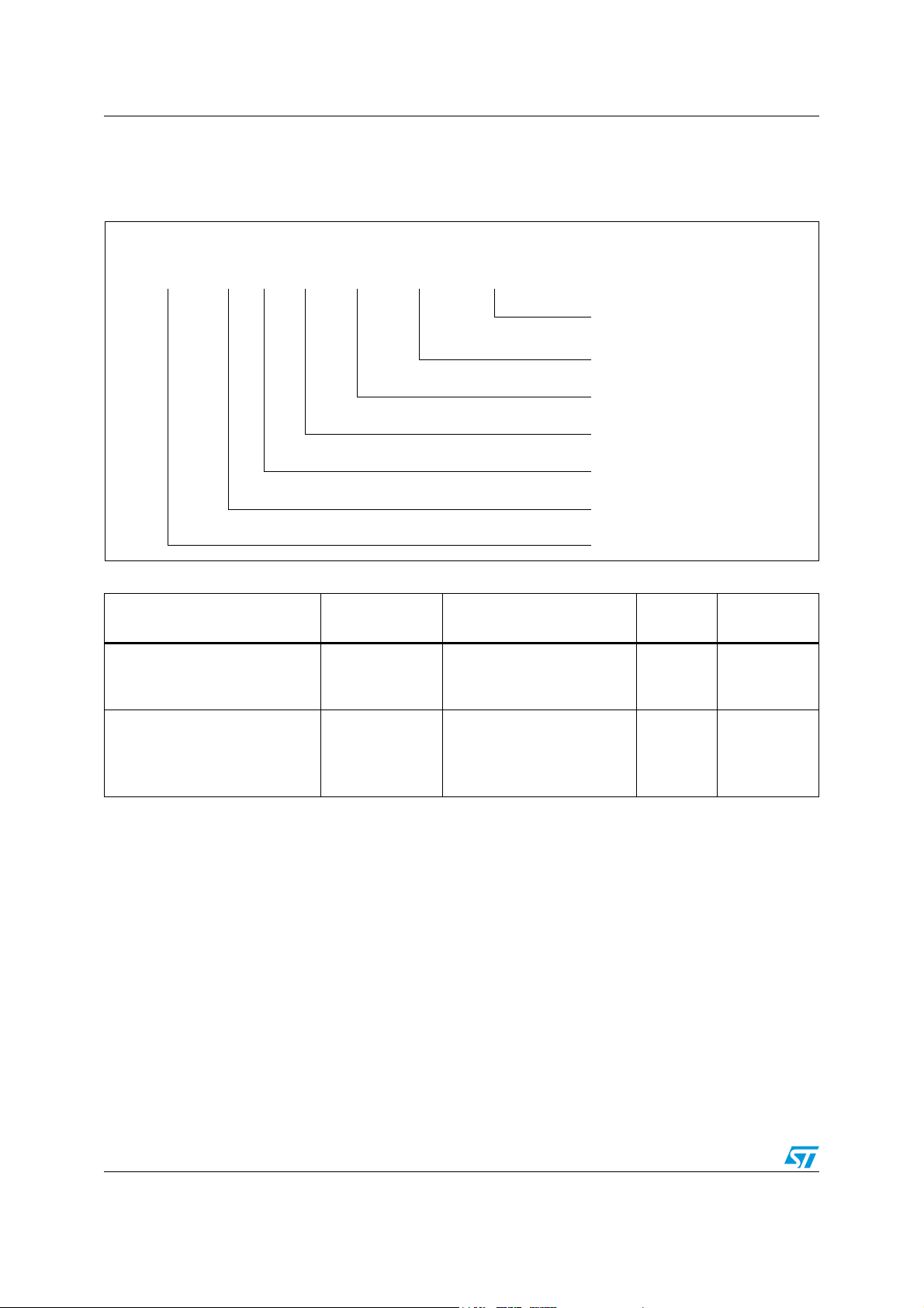
2.2 Block diagram
Figure 1 shows the block diagram of the SPC56EL60.
Figure 1. SPC56EL60 block diagram
308
6:7
(&60
670
,17&
6(0$
H'0$
0HPRU\3URWHFWLRQ8QLW 0HPRU\3URWHFWLRQ8QLW
(&&ORJLFIRU65$0 (&&ORJLFIRU65$0
3%5,'*(
76(16 76(16
U
%$ 0
66&0
)0 3 //
6HFRQGD \ 3//
H]
,&$&+(
&URVVEDU6ZLWFK
5& 2 6&
,
63(
9/(
008
)ODVKPHPRU\
(&&ELWVORJLF
&0 8
&0 8
5&
&0 8
-7$*
-7$*
1H[XV
1H[XV
)OH[5D\
5&
5&
H]
63(
9/(
008
,&$&+(
&URVVEDU6ZLWFK
5&
65$0
(&&ELWV
308
6:7
(&60
670
,17&
6(0$
H'0$
3%5,'*(
&5&
,
37
)
,
68/
;26&
$'&
$'&
:DNH8S
&78
H[3 : 0)
H[3 : 0
O
O
)
/,1)OH['
0&
3%5,'*(
3,7
308
5&
57&
6(0$
6,8/
66&0
670
6:*
6:7
76(16
;26&
$'&
%$0
&08
&5&
&78
'63,
(&&
(&60
H'0$
)&&8
)OH[&$1
)03//
,17&
,5&26&
-7$*
0&
±$QDORJWR'LJLWDO&RQYHUWHU
±%RRW$VVLVW0RGXOH
±&ORFN0RQLWRULQJ8QLW
±&\FOLF5HGXQGDQF\&KHFNXQLW
±&URVV7ULJJHULQJ8QLW
±6HULDO3HULSKHUDOV,QWHUIDFH
±(UURU&RUUHFWLRQ&RGH
±(UURU&RUUHFWLRQ6WDWXV0RGXOH
±(QKDQFHG'LUHFW0HPRU\$FFHVVFRQWUROOHU
±)DXOW&ROOHFWLRQDQG&RQWURO8QLW
±&RQWUROOHU$UHD1HWZRUNFRQWUROOHU
±)UHTXHQF\0RGXODWHG3KDVH/RFNHG/RRS
±,QWHUUXSW&RQWUROOHU
±,QWHUQDO5&2VFLOODWRU
±-RLQW7HVW$FWLRQ*URXSLQWHUIDFH
9/38 Doc ID 15461 Rev 5
7U
H[&$ 1
O
HLPH
)
1
$
H['
H['
O
O
&
[
H
1)
O
,1 )
,
)
/
/
U
H
P
L
L
7
H7 PHU
H
±/,1FRQWUROOHUZLWK'0$VXSSRUW
±0RGH(QWU\&ORFN5HVHW3RZHU
±3HULSKHUDOEULGJH
±3HULRGLF,QWHUUXSW7LPHU
±3RZHU0DQDJHPHQW8QLW
±5HGXQGDQF\&KHFNHU
±5HDO7LPH&ORFN
±6HPDSKRUH8QLW
±6\VWHP,QWHJUDWLRQ8QLW/LWH
±6\VWHP6WDWXVDQG&RQILJXUDWLRQ0RGXOH
± 6\VWHP7LPHU0RGXOH
±6LQH:DYH*HQHUDWRU
±6RIWZDUH:DWFKGRJ7LPHU
±7HPSHUDWXUH6HQVRU
±&U\VWDO2VFLOODWRU
,
'63,
'63,'63
$*9
)&&8
6:*
Page 10

SPC56EL60L3, SPC56EL60L5 Features
2.3 Operating parameters
The SPC56EL60 operating parameters are listed as follows:
● Operating range 0 – 120 MHz
● –40 to 150 °C junction temperature
● Fabricated in 90 nm low power process
● 1.2 V internal logic
● Internal voltage regulator (VREG) with integrated ballast transistor
– Single-supply designs offering high integration level to the customer
– Possibility to use external ballast transistor and for KGD bypass internal ballast
transistor
● 3.3 V ±10% for digital I/O input supply voltage
● Low power design
– Dynamic clock gating of core and peripherals
– Software controlled clock gating of peripherals
– Power consumption less than 400 mA
● Selectable current slew rate (slow/medium/fast)
● 3.3 V ± 10% Nexus pin rail. Same as digital I/O rail
● Unused pins configurable as GPIO or GPI for unused A/D channel inputs
● 3.3–5 V ±10% for A/Donverter reference and analog input pins
● Designed with EMI reduction techniques
– Phase-locked loop (PLL)
– System clock with frequency modulation
– On-chip by-pass capacitance
– Software selectable current slew rate control
– Schmitt trigger on selected inputs
● Configurable pins
– Selectable pull-up, pull-down or no pull on all pins on all SIU controlled pins
– Selectable open drain
● Redundant temperature sensors in separate safety channels
● Multiple low/high voltage detector and inhibit units
– High voltage detection and inhibit with off-line testing capability on 1.2 V only
– Low voltage detection and inhibit with off-line testing capability on 1.2 V and 3.3 V
supply
● Redundant bandgap to duplicate internal reference
● Deep N-well and wide column multiplexing where required to reduce Soft Error Rate
(SER) effect for SRAM
● Physical separation of replicated functional blocks achieved by layout
Doc ID 15461 Rev 5 10/38
Page 11

Features SPC56EL60L3, SPC56EL60L5
2.4 Modes of operation
SPC56EL60 devices can operate in two modes of operation:
● Lock Step Mode (LSM)
● Decoupled Parallel Mode (DPM)
One of the two modes is statically selected at power-up. The selected mode may be
changed only going through a full power-on reset.
2.4.1 Lock Step Mode (LSM)
Lock Step Mode (LSM) allows reaching the highest safety level. It has been defined to allow
reaching SIL3 with minimum software overhead.
The Sphere of Replication (SoR) refers to a set of replicated IP modules where at the
outputs a formal check is performed to ensure that the same operations or transactions are
executed on a clock per clock basis (Lock Step Mode of operation).
The current concept assumes as premise that the most important goal for a functional safety
SIL3-capable device is to detect (or diagnose) faults as they leave the SoR. In fact, a fault as
long as it remains confined within the SoR and therefore does not generate an action visible
outside the SoC or influence the effective operability of the periphery (and so the ECU), is
not to be considered as a dangerous fault.
The presence of checkers (RC) at the outputs of the SoR for the periphery bus, the Flashmemory subsystem and the SRAM subsystem represents a minimum guarantee that noncommon cause faults are detected when the two channels redundantly are merged into a
single actuator or recipient, on the action that is to be performed.
2.4.2 Decoupled Parallel Mode (DPM)
In Decoupled Parallel Mode (DPM), each CPU core and connected channel run
independently from the other one and redundancy checkers (RC) are disabled.
The DPM mode increased performances can be estimated in first approximation as about
1.6× the performance of the LSM mode at the same frequency for shared program flash
configuration (up to 2×, depending on software).
SPC56EL60 devices support only static configuration at power-on (either LSM or DPM).
2.5 Mode-specific performance parameters
● LSM:
– Up to 240 million integer instructions per second (dual integer unit)
– Up to 240 million floating point instructions per second (FPU)
– Up to 480 million multiply and accumulate instructions per second (SPE)
● DPM:
– 384–480 million integer/floating point instructions per second
– 768–960 million multiply and accumulate instructions per second
11/38 Doc ID 15461 Rev 5
Page 12

SPC56EL60L3, SPC56EL60L5 Features
2.6 Functional safety suitability
The SPC56EL60 has been successfully assessed by Exida Certification (Official
Certification issued on Nov. 30th 2007) to be fit for purpose to achieve a safety integrity
level 3 (SIL3) as per IEC61508-part 2 standard with an overall SoC PFH of 0.1 FIT in LSM
mode.
The mode of operation which allows to reach the highest safety level with minimum software
requirement is the Lock Step mode (LSM).
● High-performance e200z4d dual core
– 32-bit Power Architecture technology CPU
– Core frequency as high as 120 MHz
– Dual issue five-stage pipeline core
– Variable Length Encoding (VLE)
– Memory Management Unit (MMU)
– 4 KB instruction cache with error detection code
– Signal processing engine (SPE)
● Memory available
– 1 MB Flash memory with ECC
– 128 KB on-chip SRAM with ECC
– Built-in RWW capabilities for EEPROM emulation
● SIL3/ASILD innovative safety concept: LockStep mode and Fail-safe protection
– Sphere of replication (SoR) for key components (such as CPU core, DMA,
crossbar switch)
– Fault collection and control unit (FCCU)
– Redundancy control and checker unit (RCCU) on outputs of the SoR connected to
FCCU
– Boot-time Built-In Self-Test for Memory (MBIST) and Logic (LBIST) triggered by
hardware
– Boot-time Built-In Self-Test for ADC and Flash memory triggered by software
– Replicated safety enhanced watchdog
– Replicated junction temperature sensor
– Non-maskable interrupt (NMI)
– 16-region memory protection unit (MPU)
– Clock monitoring units (CMU)
– Power management unit (PMU)
– Cyclic redundancy check (CRC) unit
● Decoupled Parallel mode for high performance use of replicated cores
● Nexus Class 3+ interface
● Interrupts
– Replicated 16-priority controller
– Replicated 16-channel eDMA controller
Doc ID 15461 Rev 5 12/38
Page 13

Features SPC56EL60L3, SPC56EL60L5
● GPIOs individually programmable as input, output or special function
● Three 6-channel general-purpose eTimer units
● 2 FlexPWM units: four 16-bit channels per module
● Communications interfaces
– 2 LINFlexD channels
– 3 DSPI channels with automatic chip select generation
– 2 FlexCAN interfaces (2.0B Active) with 32 message objects
– FlexRay module (V2.1 Rev. A) with 2 channels, 64 message buffers and data rates
up to 10 Mbit/s
● Two 12-bit analog-to-digital converters (ADCs)
– 16 input channels
– Programmable cross triggering unit (CTU) to synchronize ADCs conversion with
timer and PWM
● Sine wave generator (D/A with low pass filter)
● On-chip CAN/UART bootstrap loader
● Single 3.0 V to 3.6 V voltage supply
● Ambient temperature range –40 °C to 125 °C
● Junction temperature range –40 °C to 150 °C
13/38 Doc ID 15461 Rev 5
Page 14

SPC56EL60L3, SPC56EL60L5 Features
2.7 Feature details
2.7.1 High-performance e200z4d core
The e200z4d Power Architecture core provides the following features:
● 2 independent execution units, both supporting fixed-point and floating-point operations
● Dual issue 32-bit Power Architecture technology compliant
– 5-stage pipeline (IF, DEC, EX1, EX2, WB)
– In-order execution and instruction retirement
● Full support for Power Architecture instruction set and Variable Length Encoding (VLE)
– Mix of classic 32-bit and 16-bit instruction allowed
– Optimization of code size possible
● Thirty-two 64-bit general purpose registers (GPRs)
● Harvard bus (32-bit address, 64-bit data)
– I-Bus interface capable of one outstanding transaction plus one piped with no wait-
on-data return
– D-Bus interface capable of two transactions outstanding to fill AHB pipe
● I-cache and I-cache controller: 4 KB, 256-bit cache line (programmable for 2- or 4-way)
● No data cache
● 16-entry MMU
● 8-entry branch table buffer
● Branch look-ahead instruction buffer to accelerate branching
● Dedicated branch address calculator
● 3 cycles worst case for missed branch
● Load/store unit
– Fully pipelined
– Single-cycle load latency
– Big- and little-endian modes supported
– Misaligned access support
– Single stall cycle on load to use
● Single-cycle throughput (two-cycle latency) integer 32 × 32 multiplication
● 4–14 cycles integer 32 × 32 division (average division on various benchmark of nine
cycles)
● Single precision floating-point unit
– 1 cycle throughput (2-cycle latency) floating-point 32 × 32 multiplication
– Target 9 cycles (worst case acceptable is 12 cycles) through put floating-point 32 ×
32 division
– Special square root and min/max function implemented
● Signal processing support: APU-SPE 1.1: support for vectorized mode: as many as two
floating-point instructions per clock
● Vectored interrupt support
● Reservation instruction to support read-modify-write constructs
● Extensive system development and tracing support via Nexus debug port
Doc ID 15461 Rev 5 14/38
Page 15

Features SPC56EL60L3, SPC56EL60L5
2.7.2 Crossbar switch (XBAR)
The XBAR multi-port crossbar switch supports simultaneous connections between four
master ports and three slave ports. The crossbar supports a 32-bit address bus width and a
64-bit data bus width.
The crossbar allows four concurrent transactions to occur from any master port to any slave
port, although one of those transfers must be an instruction fetch from internal Flash
memory. If a slave port is simultaneously requested by more than one master port,
arbitration logic selects the higher priority master and grants it ownership of the slave port.
All other masters requesting that slave port are stalled until the higher priority master
completes its transactions.
The crossbar provides the following features:
● 4 masters and 3 slaves supported per each replicated crossbar
– Masters allocation for each crossbar: e200z4d core with two independent bus
interface units (BIU) for I and D access (2 masters), one DMA, one FlexRay
– Slaves allocation for each crossbar: a redundant Flash-memory controller with 2
slave ports to guarantee maximum flexibility to handle Instruction and Data array,
one redundant SRAM controller with 1 slave port each and 1 redundant peripheral
bus bridge
● 32-bit address bus and 64-bit data bus
● Programmable arbitration priority: requesting masters can be treated with equal priority
and are granted access to a slave port in round-robin method, based upon the ID of the
last master to be granted access or a priority order can be assigned by software at
application run time
● Temporary dynamic priority elevation of masters
The XBAR is replicated for each processor.
2.7.3 Memory Protection Unit (MPU)
The Memory Protection Unit splits the physical memory into 16 different regions. Each
master (eDMA, FlexRay, CPU) can be assigned different access rights to each region.
● 16-region MPU with concurrent checks against each master access
● 32-byte granularity for protected address region
The memory protection unit is replicated for each processor.
2.7.4 Enhanced Direct Memory Access (eDMA)
The enhanced direct memory access (eDMA) controller is a second-generation module
capable of performing complex data movements via 16 programmable channels, with
minimal intervention from the host processor. The hardware microarchitecture includes a
DMA engine which performs source and destination address calculations, and the actual
data movement operations, along with an SRAM-based memory containing the transfer
control descriptors (TCD) for the channels. This implementation is used to minimize the
overall block size.
15/38 Doc ID 15461 Rev 5
Page 16

SPC56EL60L3, SPC56EL60L5 Features
The eDMA module provides the following features:
● 16 channels supporting 8-, 16-, and 32-bit value single or block transfers
● Support variable sized queues and circular buffered queue
● Source and destination address registers independently configured to post-increment
or stay constant
● Support major and minor loop offset
● Support minor and major loop done signals
● DMA task initiated either by hardware requestor or by software
● Each DMA task can optionally generate an interrupt at completion and retirement of the
task
● Signal to indicate closure of last minor loop
● Transfer control descriptors mapped inside the SRAM
The eDMA controller is replicated for each processor.
2.7.5 On-chip Flash memory with ECC
This device includes programmable, non-volatile Flash memory. The non-volatile memory
(NVM) can be used for instruction storage or data storage, or both. The Flash memory
module interfaces with the system bus through a dedicated Flash memory array controller. It
supports a 64-bit data bus width at the system bus port, and a 128-bit read data interface to
flash memory. The module contains four 128-bit prefetch buffers. Prefetch buffer hits allow
no-wait responses. Buffer misses incur a 3 wait state response at 120 MHz.
The Flash memory module provides the following features
● 1 MB of Flash memory in unique multi-partitioned hard macro
● Sectorization: 16 KB + 2 × 48 KB + 16 KB + 2 × 64 KB + 2 × 128 KB + 2 × 256 KB
● EEPROM emulation (in software) within same module but on different partition
● 16 KB test sector and 16 KB shadow block for test, censorship device and user option
bits
● Wait states:
– 3 wait states for frequencies ≤ 120 MHz
– 2wait states for frequencies ≤ 80 MHz
– 1 wait states for frequencies ≤ 60 MHz
● Flash memory line 128-bit wide with 8-bit ECC on 64-bit word (total 144 bits)
● Accessed via a 64-bit wide bus for write and a 128-bit wide array for read operations
● 1-bit error correction, 2-bit error detection
Doc ID 15461 Rev 5 16/38
Page 17

Features SPC56EL60L3, SPC56EL60L5
2.7.6 On-chip SRAM with ECC
The SPC56EL60 SRAM provides a general-purpose single port memory.
ECC handling is done on a 32-bit boundary for data and it is extended to the address to
have the highest possible diagnostic coverage including the array internal address decoder.
The SRAM module provides the following features:
● System SRAM: 128 KB
● ECC on 32-bit word (syndrome of 7 bits): ECC covers SRAM bus address
● 1-bit error correction, 2-bit error detection
● Wait states:
– 1 wait state at ≤ 120 MHz
– 0 wait state at ≤ 80 MHz 60 MHz
2.7.7 Platform Flash memory controller
The following list summarizes the key features of the Flash memory controller:
● Single AHB port interface supports a 64-bit data bus. All AHB aligned and unaligned
reads within the 32-bit container are supported. Only aligned word writes are
supported.
● Array interfaces support a 128-bit read data bus and a 64-bit write data bus for each
bank.
● Code Flash (bank0) interface provides configurable read buffering and page prefetch
support: four page-read buffers (each 128 bits wide) and a prefetch controller support
speculative reading and optimized Flash access.
● Single-cycle read responses (0 AHB data-phase wait states) for hits in the buffers. The
buffers implement a least-recently-used replacement algorithm to maximize
performance.
● Data Flash (bank1) interface includes a 128-bit register to temporarily hold a single
Flash page. This logic supports single-cycle read responses (0 AHB data-phase wait
states) for accesses that hit in the holding register: no prefetch support is provided for
this bank.
● Programmable response for read-while-write sequences including support for stall-
while-write, optional stall notification interrupt, optional Flash operation abort, and
optional abort notification interrupt.
● Separate and independent configurable access timing (on a per bank basis) to support
use across a wide range of platforms and frequencies.
● Support of address-based read access timing for emulation of other memory types.
● Support for reporting of single- and multi-bit error events.
● Typical operating configuration loaded into programming model by system reset.
The platform Flash controller is replicated for each processor.
17/38 Doc ID 15461 Rev 5
Page 18
SPC56EL60L3, SPC56EL60L5 Features
2.7.8 Platform Static RAM Controller (SRAMC)
The SRAMC module is the platform SRAM array controller, with integrated error detection
and correction.
The main features of the SRAMC provide connectivity for the following interfaces:
● XBAR Slave Port (64-bit data path)
● ECSM (ECC Error Reporting, error injection and configuration)
● SRAM array
The following functions are implemented:
● ECC encoding (32-bit boundary for data and complete address bus)
● ECC decoding (32-bit boundary and entire address)
● Address translation from the AHB protocol on the XBAR to the SRAM array
The platform SRAM controller is replicated for each processor.
2.7.9 Memory subsystem access time
Every memory access the CPU performs requires at least one system clock cycle for the
data phase of the access. Slower memories or peripherals may require additional data
phase wait states. Additional data phase wait states may also occur if the slave being
accessed is not parked on the requesting master in the crossbar.
Ta bl e 2 shows the number of additional data phase wait states required for a range of
memory accesses.
Table 2. Platform memory access time summary
e200z4d instruction fetch 0 Flash memory prefetch buffer hit (page hit)
e200z4d instruction fetch 3
e200z4d data read 0 – 1 SRAM read
e200z4d data write 0 SRAM 32-bit write
e200z4d data write 0 SRAM 64-bit write (executed as 2 x 32-bit writes)
e200z4d data write 0 – 2
e200z4d data Flash memory
read
e200z4d data Flash memory
read
AHB transfer
Data phase
wait states
Flash memory prefetch buffer miss (based on 4-cycle random
flash array access time)
SRAM 8-,16-bit write
(Read-modify-Write for ECC)
0 Flash memory prefetch buffer hit (page hit)
3
Flash memory prefetch buffer miss (at 120 MHz; includes 1 cycle
of program Flash memory controller arbitration)
Description
2.7.10 Error Correction Status Module (ECSM)
The ECSM on this device manages the ECC configuration and reporting for the platform
memories (Flash memory and SRAM). It does not implement the actual ECC calculation. A
Doc ID 15461 Rev 5 18/38
Page 19

Features SPC56EL60L3, SPC56EL60L5
detected error (double error for Flash memory or SRAM) is also reported to the FCCU. The
following errors and indications are reported into the ECSM dedicated registers:
● ECC error status and configuration for Flash memory and SRAM
● ECC error reporting for Flash memory
● ECC error reporting for SRAM
● ECC error injection for SRAM
2.7.11 Peripheral bridge (PBRIDGE)
The PBRIDGE implements the following features:
● Duplicated periphery
● Master access privilege level (per master: read access enable; write access enable)
● Checker applied on PBRIDGE output toward periphery
● Byte endianess swap capability
2.7.12 Interrupt Controller (INTC)
The INTC (interrupt controller) provides priority-based preemptive scheduling of interrupt
requests, suitable for statically scheduled hard real-time systems.
For high-priority interrupt requests, the time from the assertion of the interrupt request from
the peripheral to when the processor is executing the interrupt service routine (ISR) has
been minimized. The INTC provides a unique vector for each interrupt request source for
quick determination of which ISR needs to be executed. It also provides an ample number of
priorities so that lower priority ISRs do not delay the execution of higher priority ISRs. To
allow the appropriate priorities for each source of interrupt request, the priority of each
interrupt request is software configurable.
The INTC supports the priority ceiling protocol for coherent accesses. By providing a
modifiable priority mask, the priority can be raised temporarily so that all tasks which share
the resource can not preempt each other.
The INTC provides the following features:
● Duplicated periphery
● Unique 9-bit vector per interrupt source
● 16 priority levels with fixed hardware arbitration within priority levels for each interrupt
source
● Priority elevation for shared resource
The INTC is replicated for each processor.
19/38 Doc ID 15461 Rev 5
Page 20

SPC56EL60L3, SPC56EL60L5 Features
2.7.13 System clocks and clock generation
The following list summarizes the system clock and clock generation on this device:
● Lock status continuously monitored by lock detect circuitry
● Loss-of-clock (LOC) detection for reference and feedback clocks
● On-chip loop filter (for improved electromagnetic interference performance and fewer
external components required)
● Programmable output clock divider of system clock (÷1, ÷2, ÷4, ÷8)
● FlexPWM module and as many as three eTimer modules running on an auxiliary clock
independent from system clock (with max frequency 120 MHz)
● On-chip crystal oscillator with automatic level control
● Dedicated internal 16 MHz internal RC oscillator for rapid start-up: supports automated
frequency trimming by hardware during device startup and by user application
● Auxiliary clock domain for motor control periphery (FlexPWM, eTimer, CTU, ADC, and
SWG)
2.7.14 Frequency-Modulated Phase-Locked Loop (FMPLL)
Two FMPLLs are available on each device.
Each FMPLL allows the user to generate high speed system clocks starting from a minimum
reference of 4 MHz input clock. Further, the FMPLL supports programmable frequency
modulation of the system clock. The PLL multiplication factor, output clock divider ratio are
all software configurable. The FMPLLs have the following major features:
● Input frequency: 4–40 MHz continuous range (limited by the crystal oscillator)
● Voltage controlled oscillator (VCO) range: 256–512 MHz
● Frequency modulation via software control to reduce and control emission peaks
– Modulation depth ±2% if centered or 0% to – 4% if downshifted via software
control register
– Modulation frequency: triangular modulation with 25 kHz nominal rate
● Option to switch modulation on and off via software interface
● Reduced frequency divider (RFD) for reduced frequency operation without re-lock
● 3 modes of operation
– Bypass mode
– Normal FMPLL mode with crystal reference (default)
– Normal FMPLL mode with external reference
● Lock monitor circuitry with lock status
● Loss-of-lock detection for reference and feedback clocks
● Self-clocked mode (SCM) operation
Doc ID 15461 Rev 5 20/38
Page 21

Features SPC56EL60L3, SPC56EL60L5
● On-chip loop filter
● Auxiliary FMPLL
– Used for FlexRay due to precise symbol rate requirement by the protocol
– Used for motor control periphery and connected IP (A/D digital interface CTU) to
allow independent frequencies of operation for PWM and timers and jitter-free
control
– Option to enable/disable modulation to avoid protocol violation on jitter and/or
potential unadjusted error in electric motor control loop
– Allows to run motor control periphery at different (precisely lower, equal or higher
as required) frequency than the system to ensure higher resolution
2.7.15 Main oscillator
The main oscillator provides these features:
● Input frequency range 4–40 MHz
● Crystal input mode
● External reference clock (3.3 V) input mode
● FMPLL reference
2.7.16 Internal Reference Clock (RC) oscillator
The architecture uses constant current charging of a capacitor. The voltage at the capacitor
is compared to the stable bandgap reference voltage. The RC oscillator is the device safe
clock.
The RC oscillator provides these features:
● Nominal frequency 16 MHz
● ±5 % variation over voltage and temperature after process trim
● Clock output of the RC oscillator serves as system clock source in case loss of lock or
loss of clock is detected by the FMPLL
● RC oscillator is used as the default system clock during startup and can be used as
back-up input source of FMPLL(s) in case XOSC fails
2.7.17 Clock, reset, power, mode and test control modules (MC_CGM, MC_RGM, MC_PCU, and MC_ME)
These modules provide the following:
● Clock gating and clock distribution control
● Halt, stop mode control
● Flexible configurable system and auxiliary clock dividers
● Various execution modes
– HALT and STOP mode as reduced activity low power mode
– Reset, Idle, Test, Safe
– Various RUN modes with software selectable powered modules
– No standby mode implemented (no internal switchable power domains)
21/38 Doc ID 15461 Rev 5
Page 22

SPC56EL60L3, SPC56EL60L5 Features
2.7.18 Periodic Interrupt Timer Module (PIT)
The PIT module implements the following features:
● 4 general purpose interrupt timers
● 32-bit counter resolution
● Can be used for software tick or DMA trigger operation
2.7.19 System Timer Module (STM)
The STM implements the following features:
● Up-counter with four output compare registers
● OS task protection and hardware tick implementation per AUTOSAR
(a)
requirement
The STM is replicated for each processor.
2.7.20 Software Watchdog Timer (SWT)
This module implements the following features:
● Fault tolerant output
● Safe internal RC oscillator as reference clock
● Windowed watchdog
● Program flow control monitor with 16-bit pseudorandom key generation
● Allows a high level of safety (SIL3 monitor)
The SWT module is replicated for each processor.
2.7.21 Fault Collection and Control Unit (FCCU)
The FCCU module has the following features:
● Redundant collection of hardware checker results
● Redundant collection of error information and latch of faults from critical modules on
the device
● Collection of self-test results
● Configurable and graded fault control
– Internal reactions (no internal reaction, IRQ, Functional Reset, Destructive Reset,
or Safe mode entered)
– External reaction (failure is reported to the external/surrounding system via
configurable output pins)
2.7.22 System Integration Unit Lite (SIUL)
The SIUL controls MCU reset configuration, pad configuration, external interrupt, general
purpose I/O (GPIO), internal peripheral multiplexing, and the system reset operation. The
reset configuration block contains the external pin boot configuration logic. The pad
configuration block controls the static electrical characteristics of I/O pins. The GPIO block
provides uniform and discrete input/output control of the I/O pins of the MCU.
a. Automotive Open System Architecture
Doc ID 15461 Rev 5 22/38
Page 23

Features SPC56EL60L3, SPC56EL60L5
The SIU provides the following features:
● Centralized pad control on per pin basis
– Pin function selection
– Configurable weak pull-up/down
– Configurable slew rate control (slow/medium/fast)
– Hysteresis on GPIO pins
– Configurable automatic safe mode pad control
● Input filtering for external interrupts
2.7.23 Non-Maskable Interrupt (NMI)
The non-maskable interrupt with de-glitching filter supports high priority core exceptions.
2.7.24 Boot Assist Module (BAM)
The BAM is a block of read-only memory with hard-coded content. The BAM program is
executed only if serial booting mode is selected via boot configuration pins.
The BAM provides the following features:
● Enables booting via serial mode (FlexCAN or LINFlex-UART)
● Supports programmable 64-bit password protection for serial boot mode
● Supports serial bootloading of either classic Power Architecture code (default) or VLE
code
● Automatic switch to serial boot mode if internal Flash memory is blank or invalid
2.7.25 System Status and Configuration Module (SSCM)
The SSCM on this device features the following:
● System configuration and status
● Debug port status and debug port enable
● Multiple boot code starting locations out of reset through implementation of search for
valid Reset Configuration Half Word
● Sets up the MMU to allow user boot code to execute as either classic Power
Architecture code (default) or as VLE code out of Flash memory
● Triggering of device self-tests during reset phase of device boot
2.7.26 FlexCAN
The FlexCAN module is a communication controller implementing the CAN protocol
according to Bosch Specification version 2.0B. The CAN protocol was designed to be used
primarily as a vehicle serial data bus, meeting the specific requirements of this field: realtime processing, reliable operation in the EMI environment of a vehicle, cost-effectiveness
and required bandwidth.
23/38 Doc ID 15461 Rev 5
Page 24

SPC56EL60L3, SPC56EL60L5 Features
The FlexCAN module provides the following features:
● Full implementation of the CAN protocol specification, version 2.0B
– Standard data and remote frames
– Extended data and remote frames
– 0 to 8 bytes data length
– Programmable bit rate as fast as 1Mbit/s
● 32 message buffers of 0 to 8 bytes data length
● Each message buffer configurable as receive or transmit buffer, all supporting standard
and extended messages
● Programmable loop-back mode supporting self-test operation
● 3 programmable mask registers
● Programmable transmit-first scheme: lowest ID or lowest buffer number
● Time stamp based on 16-bit free-running timer
● Global network time, synchronized by a specific message
● Maskable interrupts
● Independent of the transmission medium (an external transceiver is assumed)
● High immunity to EMI
● Short latency time due to an arbitration scheme for high priority messages
● Transmit features
– Supports configuration of multiple mailboxes to form message queues of scalable
depth
– Arbitration scheme according to message ID or message buffer number
– Internal arbitration to guarantee no inner or outer priority inversion
– Transmit abort procedure and notification
● Receive features
– Individual programmable filters for each mailbox
– 8 mailboxes configurable as a 6-entry receive FIFO
– 8 programmable acceptance filters for receive FIFO
● Programmable clock source
– System clock
– Direct oscillator clock to avoid FMPLL jitter
Doc ID 15461 Rev 5 24/38
Page 25

Features SPC56EL60L3, SPC56EL60L5
2.7.27 FlexRay
The FlexRay module provides the following features:
● Full implementation of FlexRay Protocol Specification 2.1 Rev. A
● 64 configurable message buffers can be handled
● Dual channel or single channel mode of operation, each as fast as 10 Mbit/s data rate
● Message buffers configurable as transmit or receive
● Message buffer size configurable
● Message filtering for all message buffers based on Frame ID, cycle count, and
message ID
● Programmable acceptance filters for receive FIFO
● Message buffer header, status and payload data stored in system memory (SRAM)
● Internal FlexRay memories have error detection and correction
25/38 Doc ID 15461 Rev 5
Page 26

SPC56EL60L3, SPC56EL60L5 Features
2.7.28 Serial communication interface module (LINFlexD)
The LINFlexD module (LINFlex with DMA support) on this device features the following:
● Supports LIN Master mode, LIN Slave mode and UART mode
● LIN state machine compliant to LIN1.3, 2.0, and 2.1 specifications
● Manages LIN frame transmission and reception without CPU intervention
● LIN features
– Autonomous LIN frame handling
– Message buffer to store as many as 8 data bytes
– Supports messages as long as 64 bytes
– Detection and flagging of LIN errors (Sync field, delimiter, ID parity, bit framing,
checksum and Time-out errors)
– Classic or extended checksum calculation
– Configurable break duration of up to 36-bit times
– Programmable baud rate prescalers (13-bit mantissa, 4-bit fractional)
– Diagnostic features (Loop back, LIN bus stuck dominant detection)
– Interrupt driven operation with 16 interrupt sources
● LIN slave mode features
– Autonomous LIN header handling
– Autonomous LIN response handling
● UART mode
– Full-duplex operation
– Standard non return-to-zero (NRZ) mark/space format
– Data buffers with 4-byte receive, 4-byte transmit
– Configurable word length (8-bit, 9-bit, or 16-bit words)
– Configurable parity scheme: none, odd, even, always 0
– Speed as fast as 2 Mbit/s
– Error detection and flagging (Parity, Noise and Framing errors)
– Interrupt driven operation with four interrupt sources
– Separate transmitter and receiver CPU interrupt sources
– 16-bit programmable baud-rate modulus counter and 16-bit fractional
– 2 receiver wake-up methods
● Support for DMA enabled transfers
2.7.29 Deserial Serial Peripheral Interface (DSPI)
The DSPI module provides a synchronous serial interface for communication between the
SPC56EL60 and external devices.
Doc ID 15461 Rev 5 26/38
Page 27

Features SPC56EL60L3, SPC56EL60L5
A DSPI module provides these features:
● Full duplex, synchronous transfers
● Master or slave operation
● Programmable master bit rates
● Programmable clock polarity and phase
● End-of-transmission interrupt flag
● Programmable transfer baud rate
● Programmable data frames from 4 to 16 bits
● As many as 8 chip select lines available, depending on package and pin multiplexing
● 4 clock and transfer attributes registers
● Chip select strobe available as alternate function on one of the chip select pins for de-
glitching
● FIFOs for buffering as many as 5 transfers on the transmit and receive side
● Queueing operation possible through use of the eDMA
● General purpose I/O functionality on pins when not used for SPI
2.7.30 FlexPWM
The pulse width modulator module (FlexPWM) contains four PWM channels, each of which
is configured to control a single half-bridge power stage. Two modules are instantiated on
the LFBGA257 device; on the LQFP144 package, only one module is present. Additionally,
four fault input channels are provided per FlexPWM module.
This PWM is capable of controlling most motor types, including:
● AC induction motors (ACIM)
● Permanent Magnet AC motors (PMAC)
● Brushless (BLDC) and brush DC motors (BDC)
● Switched (SRM) and variable reluctance motors (VRM)
● Stepper motors
A FlexPWM module implements the following features:
● 16 bits of resolution for center, edge aligned, and asymmetrical PWMs
● Maximum operating frequency as high as 120 MHz: clock source not modulated and
independent from system clock (generated via auxiliary FMPLL)
● Fine granularity control for enhanced resolution of the PWM period
● PWM outputs can operate as complementary pairs or independent channels
● Ability to accept signed numbers for PWM generation
● Independent control of both edges of each PWM output
● Synchronization to external hardware or other PWM supported
27/38 Doc ID 15461 Rev 5
Page 28

SPC56EL60L3, SPC56EL60L5 Features
● Double buffered PWM registers
– Integral reload rates from 1 to 16
– Half cycle reload capability
● Multiple ADC trigger events can be generated per PWM cycle via hardware
● Fault inputs can be assigned to control multiple PWM outputs
● Programmable filters for fault inputs
● Independently programmable PWM output polarity
● Independent top and bottom deadtime insertion
● Each complementary pair can operate with its own PWM frequency and deadtime
values
● Individual software control for each PWM output
● All outputs can be forced to a value simultaneously
● PWMX pin can optionally output a third signal from each channel
● Channels not used for PWM generation can be used for buffered output compare
functions
● Channels not used for PWM generation can be used for input capture functions
● Enhanced dual edge capture functionality
● Option to supply the source for each complementary PWM signal pair from any of the
following:
– External digital pin
– Internal timer channel
– External ADC input, taking into account values set in ADC high and low limit
registers
● DMA support
Doc ID 15461 Rev 5 28/38
Page 29

Features SPC56EL60L3, SPC56EL60L5
2.7.31 eTimer module
The SPC56EL60 provides three eTimer modules on the LFBGA257 device, and two eTimer
modules on the LQFP144 package. Six 16-bit general purpose up/down timer/counters per
module are implemented with the following features:
● Maximum clock frequency 120 MHz
● Individual channel capability
– Input capture trigger
– Output compare
– Double buffer (to capture rising edge and falling edge)
– Separate prescaler for each counter
– Selectable clock source
– 0 – 100 % pulse measurement
– Rotation direction flag (Quad decoder mode)
● Maximum count rate
– Equals peripheral clock divided by 2 for external event counting
– Equals peripheral clock for internal clock counting
● Cascadeable counters
● Programmable count modulo
● Quadrature decode capabilities
● Counters can share available input pins
● Count once or repeatedly
● Preloadable counters
● Pins available as GPIO when timer functionality not in use
● DMA support
2.7.32 Sine Wave Generator (SWG)
A customized digital-to-analog converter is available to generate a sine wave based on 32
stored values for external devices (ex: resolver).
● Frequency range from 1 kHz to 50 kHz
● Sine wave amplitude from 0.47 V to 2.26 V
29/38 Doc ID 15461 Rev 5
Page 30

SPC56EL60L3, SPC56EL60L5 Features
2.7.33 Analog-to-Digital Converter module (ADC)
The ADC module features are as follows:
Analog part:
● 2 on-chip ADCs
– 12-bit resolution SAR architecture
– Same digital interface as in the SPC560P family
– A/D channels: 9 external, 3 internal and 4 shared with other A/D (total 16
channels)
– One channel dedicated to each T-sensor to enable temperature reading during
application
– Separated reference for each ADC
– Shared analog supply voltage for both ADCs
– One sample and hold unit per ADC
– Adjustable sampling and conversion time
Digital part:
● 4 analog watchdogs comparing ADC results against predefined levels (low, high,
range) before results are stored in the appropriate ADC result location
● 2 modes of operation: CPU Mode or CTU Mode
● Regular mode features
– Register based interface with the CPU: one result register per channel
– ADC state machine managing three request flows: regular command, hardware
injected command, software injected command
– Selectable priority between software and hardware injected commands
– 4 analog watchdogs comparing ADC results against predefined levels (low, high,
range)
– DMA compatible interface
● CTU mode features
– Triggered mode only
– 4 independent result queues (1 × 16 entries, 2 × 8 entries, 1 × 4 entries)
– Result alignment circuitry (left justified; right justified)
– 32-bit read mode allows to have channel ID on one of the 16-bit parts
– DMA compatible interfaces
● Built-in self-test features triggered by software
Doc ID 15461 Rev 5 30/38
Page 31

Features SPC56EL60L3, SPC56EL60L5
2.7.34 Cross Triggering Unit (CTU)
The ADC cross triggering unit allows automatic generation of ADC conversion requests on
user selected conditions without CPU load during the PWM period and with minimized CPU
load for dynamic configuration.
The CTU implements the following features:
● Cross triggering between ADC, FlexPWM, eTimer, and external pins
● Double buffered trigger generation unit with as many as 8 independent triggers
generated from external triggers
● Maximum operating frequency less than or equal to 120 MHz
● Trigger generation unit configurable in sequential mode or in triggered mode
● Trigger delay unit to compensate the delay of external low pass filter
● Double buffered global trigger unit allowing eTimer synchronization and/or ADC
command generation
● Double buffered ADC command list pointers to minimize ADC-trigger unit update
● Double buffered ADC conversion command list with as many as 24 ADC commands
● Each trigger capable of generating consecutive commands
● ADC conversion command allows control of ADC channel from each ADC, single or
synchronous sampling, independent result queue selection
● DMA support with safety features
2.7.35 Cyclic Redundancy Checker (CRC) Unit
The CRC module is a configurable multiple data flow unit to compute CRC signatures on
data written to input register.
The CRC unit has the following features:
● 3 sets of registers to allow 3 concurrent contexts with possibly different CRC
computations, each with a selectable polynomial and seed
● Computes 16- or 32-bit wide CRC on the fly (single-cycle computation) and stores
result in internal register.
The following standard CRC polynomials are implemented:
8
– x
–x
– x
● Key engine to be coupled with communication periphery where CRC application is
added to allow implementation of safe communication protocol
● Offloads core from cycle-consuming CRC and helps checking configuration signature
for safe start-up or periodic procedures
● CRC unit connected as peripheral bus on internal peripheral bus
● DMA support
+ x4+ x3+x21 [8-bit CRC] (supported on cut 2/3 only)
16
+ x12+ x5+ 1 [16-bit CRC-CCITT]
32
+ x26+ x23+ x22+ x16+ x12+ x11+ x10+ x8+ x7+ x5+ x4+ x2+ x +1
[32-bit CRC-ethernet(32)]
31/38 Doc ID 15461 Rev 5
Page 32

SPC56EL60L3, SPC56EL60L5 Features
2.7.36 Redundancy Control and Checker Unit (RCCU)
The RCCU checks all outputs of the sphere of replication (addresses, data, control signals).
It has the following features:
● Duplicated module to guarantee highest possible diagnostic coverage (check of
checker)
● Multiple times replicated IPs are used as checkers on the SoR outputs
2.7.37 Junction temperature sensor
The junction temperature sensor provides a value via an ADC channel that can be used by
software to calculate the device junction temperature.
The key parameters of the junction temperature sensor include:
● Nominal temperature range from –40 to 150 °C
● Software temperature alarm via analog ADC comparator possible
2.7.38 Nexus Port Controller (NPC)
The NPC module provides real-time development support capabilities for this device in
compliance with the IEEE-ISTO 5001-2003 standard. This development support is supplied
for MCUs without requiring external address and data pins for internal visibility.
The NPC block interfaces to the host processor and internal buses to provide development
support as per the IEEE-ISTO 5001-2008 Class 3+, including selected features from Class
4 standard.
The development support provided includes program trace, data trace, watchpoint trace,
ownership trace, run-time access to the MCUs internal memory map and access to the
Power Architecture internal registers during halt. The Nexus interface also supports a JTAG
only mode using only the JTAG pins. The following features are implemented:
● Full and reduced port modes
● MCKO (message clock out) pin
● 4 or 12 MDO (message data out) pins
● 2 MSEO (message start/end out) pins
● EVTO (event out) pin: auxiliary input port
● EVTI (event in) pin
● 5-pin JTAG port (JCOMP, TDI, TDO, TMS, and TCK): supports JTAG mode
● Host processor (e200) development support features
(b)
– Data trace via data write messaging (DWM) and data read messaging (DRM).
This allows the development tool to trace reads or writes, or both, to selected
internal memory resources.
– Ownership trace via ownership trace messaging (OTM). OTM facilitates ownership
trace by providing visibility of which process ID or operating system task is
b. 4 MDO pins on LQFP144 package, 12 MDO pins on LFBGA257 package.
Doc ID 15461 Rev 5 32/38
Page 33

Features SPC56EL60L3, SPC56EL60L5
activated. An ownership trace message is transmitted when a new process/task is
activated, allowing development tools to trace ownership flow.
– Program trace via branch trace messaging (BTM). Branch trace messaging
displays program flow discontinuities (direct branches, indirect branches,
exceptions, etc.), allowing the development tool to interpolate what transpires
between the discontinuities. Thus, static code may be traced.
– Watchpoint messaging (WPM) via the auxiliary port
– Watchpoint trigger enable of program and/or data trace messaging
– Data tracing of instruction fetches via private opcodes
2.7.39 IEEE 1149.1 JTAG Controller (JTAGC)
The JTAGC block provides the means to test chip functionality and connectivity while
remaining transparent to system logic when not in test mode. All data input to and output
from the JTAGC block is communicated in serial format. The JTAGC block is compliant with
the IEEE standard.
The JTAG controller provides the following features:
● IEEE Test Access Port (TAP) interface with five pins:
–TDI
–TMS
–TCK
–TDO
–JCOMP
● Selectable modes of operation include JTAGC/debug or normal system operation
● 5-bit instruction register that supports the following IEEE 1149.1-2001 defined
instructions:
– BYPASS
– IDCODE
–EXTEST
–SAMPLE
– SAMPLE/PRELOAD
● 3 test data registers: a bypass register, a boundary scan register, and a device
identification register. The size of the boundary scan register is parameterized to
support a variety of boundary scan chain lengths.
● TAP controller state machine that controls the operation of the data registers,
instruction register and associated circuitry
33/38 Doc ID 15461 Rev 5
Page 34

SPC56EL60L3, SPC56EL60L5 Features
2.7.40 Voltage regulator / Power Management Unit (PMU)
The on-chip voltage regulator module provides the following features:
● Single external rail required
● Single high supply required: nominal 3.3 V both for packaged and Known Good Die
option
– Packaged option requires external ballast transistor due to reduced dissipation
capacity at high temperature but can use embedded transistor if power dissipation
is maintained within package dissipation capacity (lower frequency of operation)
– Known Good Die option uses embedded ballast transistor as dissipation capacity
is increased to reduce system cost
● All I/Os are at same voltage as external supply (3.3 V nominal)
● Duplicated Low-Voltage Detectors (LVD) to guarantee proper operation at all stages
(reset, configuration, normal operation) and, to maximize safety coverage, one LVD can
be tested while the other operates (on-line self-testing feature)
2.7.41 Built-In Self-Test (BIST) capability
This device includes the following protection against latent faults:
● Boot-time Memory Built-In Self-Test (MBIST)
● Boot-time scan-based Logic Built-In Self-Test (LBIST)
● Run-time ADC Built-In Self-Test (BIST)
● Run-time Built-In Self Test of LVDs
Doc ID 15461 Rev 5 34/38
Page 35
Ordering information SPC56EL60L3, SPC56EL60L5
3 Ordering information
Figure 2. Commercial product code structure
Example code:
SPC56 60EL CL5 BF
Product identifier
MemoryCore Family TemperaturePackage Device Options.
C=80MHz
B=>120MHz
F = Full-featured
B = –40 °C to 105 °C
C = –40 °C to 125 °C
L3 = LQFP100
L5 = LQFP144
C3 = LFBGA257
60 = 1 MB Flash memory
L = this device family
E = e200z4d dual core
4 = single core
SPC56 = Power Architecture in 90 nm
Table 3. Order codes
Order code Flash/SRAM Package
Speed
(MHz)
SPC564L60L3BCF 1 MB/128 KB LQFP100 80
SPC56EL60L5CBF 1 MB/128 KB LQFP144 120
1. This speed rating does not include the ±2% for frequency modulation.
(1)
Other
features
Single core
FlexRay
–40–105 °C
Dual core
FlexRay
3.3 V
–40–125 °C
35/38 Doc ID 15461 Rev 5
Page 36

SPC56EL60L3, SPC56EL60L5 Revision history
4 Revision history
Table 4. Document revision history
Date Revision Description
09-Mar-2009 1 Initial release.
06-Oct-2009 2
Editorial changes.
Added information about the 257-pin BGA and KGD packages.
Updated the device-comparison table.
In the block diagram:
– Added the SEMA4 and SWG blocks.
– Added information to reflect the use of ECC logic.
In the feature summary:
– Updated final bullet to differentiate junction and ambient temp specs.
– In the ADC section, changed “11 input channels” to “16 input channels”.
In the feature details:
– Added statement that the 144-pin package has one FlexPWM.
– Removed information about the JTAG CLAMP and HIGHZ instructions (not
available on this device).
– Changed the flash memory sectorization to align with the memory map.
– Moved the “Supports serial bootloading...” feature from the SSCM section to
the BAM section.
– In the SSCM section, deleted “Detection of user boot code”.
– Added feature bullets for the Sine Wave Generator (SWG).
Revised the “Ordering information” section.
25-Feb-2010 3
Editorial changes.
Revised the 257-pin package pin pitch (was 1.4 mm, is 0.8 mm).
Added information about the 100-pin LQFP.
Changed “LINFlex” to “LINFlexD” to be consistent with the rest of the
documentation.
In the device block diagram, renamed the peripheral bridge to “PBRIDGE”.
In the feature list, revised the information for FlexRay.
In the feature details:
– Revised the information for FlexRay.
– Renamed the peripheral bridge to “PBRIDGE”.
– Revised the “Clock, reset, power, mode and test control module” section (it’s
not one module, but individual modules).
In the “Ordering information” section, added an entry for temperature code B
and removed order code SPC56EL60C3.
Doc ID 15461 Rev 5 36/38
Page 37

Revision history SPC56EL60L3, SPC56EL60L5
Table 4. Document revision history (continued)
Date Revision Description
Editorial changes.
In section 2.6, changed “As much as 128 KB on-chip SRAM” to “128 KB on-chip
SRAM”.
In the section 2.7 :
– Revised table 2 and replaced TBDs by meaningful values.
– In the section 2.7.5, changed “16 KB Test” to “16 KB test sector”, revised the
11-April-2011 4
20-April-2011 5
wait state information.
– In the section 2.7.6 added information about required RAM wait states.
– In the section 2.7.18, deleted “32-bit counter for real time interrupt, clocked
from main external oscillator” (not supported on this device).
– Added in section 2.7.19 a footnote (a.: Automotive Open System
Architecture) explaining the AUTOSAR acronym.
– In the table 3, added a footnote about frequency modulation to the “Speed
(MHz)” column heading.
Editorial changes.
In the 2.1 section added footnote regarding LBGA257 packages.
– In the 2.7.5 changed shadow sector to shadow block and 2.7.6 sections,
updated the precise information regarding wait states.
– In the 2.6 section: changed “CAN/UART/FlexRay Bootstrap loader” to
“CAN/UART bootstrap loader”.
– In the 2.7 section: changed “CAN/UART/FlexRay Bootstrap loader” to
“CAN/UART bootstrap loader”.
– In the 2.7.11 section, deleted “Write buffering for peripherals” and changed
“Master access right” to “Master access privilege level”.
– Added bullet regarding HALT and STOP in the 2.7.17 section.
– In the 2.7.24 and 2.7.25 sections, changed “classic PowerPC Book E code”
to “Power Architecture code”.
– In the 2.7.33 section, changed “Motor control mode“ to “CTU mode“ to be
consistent with the nomenclature used in the Reference Manual.
– In the 2.7.35 section, added information about the 8-bit polynomial
implemented on cut2.
– In the 2.7.37 section, updated the modes .
– In 2.7.38 section changed IEEE-ISTO 5001-2008 to IEEE-ISTO 5001-2003.
– Removed the third dimension measurements from the front page graphics.
37/38 Doc ID 15461 Rev 5
Page 38

SPC56EL60L3, SPC56EL60L5
Please Read Carefully:
Information in this document is provided solely in connection with ST products. STMicroelectronics NV and its subsidiaries (“ST”) reserve the
right to make changes, corrections, modifications or improvements, to this document, and the products and services described herein at any
time, without notice.
All ST products are sold pursuant to ST’s terms and conditions of sale.
Purchasers are solely responsible for the choice, selection and use of the ST products and services described herein, and ST assumes no
liability whatsoever relating to the choice, selection or use of the ST products and services described herein.
No license, express or implied, by estoppel or otherwise, to any intellectual property rights is granted under this document. If any part of this
document refers to any third party products or services it shall not be deemed a license grant by ST for the use of such third party products
or services, or any intellectual property contained therein or considered as a warranty covering the use in any manner whatsoever of such
third party products or services or any intellectual property contained therein.
UNLESS OTHERWISE SET FORTH IN ST’S TERMS AND CONDITIONS OF SALE ST DISCLAIMS ANY EXPRESS OR IMPLIED
WARRANTY WITH RESPECT TO THE USE AND/OR SALE OF ST PRODUCTS INCLUDING WITHOUT LIMITATION IMPLIED
WARRANTIES OF MERCHANTABILITY, FITNESS FOR A PARTICULAR PURPOSE (AND THEIR EQUIVALENTS UNDER THE LAWS
OF ANY JURISDICTION), OR INFRINGEMENT OF ANY PATENT, COPYRIGHT OR OTHER INTELLECTUAL PROPERTY RIGHT.
UNLESS EXPRESSLY APPROVED IN WRITING BY AN AUTHORIZED ST REPRESENTATIVE, ST PRODUCTS ARE NOT
RECOMMENDED, AUTHORIZED OR WARRANTED FOR USE IN MILITARY, AIR CRAFT, SPACE, LIFE SAVING, OR LIFE SUSTAINING
APPLICATIONS, NOR IN PRODUCTS OR SYSTEMS WHERE FAILURE OR MALFUNCTION MAY RESULT IN PERSONAL INJURY,
DEATH, OR SEVERE PROPERTY OR ENVIRONMENTAL DAMAGE. ST PRODUCTS WHICH ARE NOT SPECIFIED AS "AUTOMOTIVE
GRADE" MAY ONLY BE USED IN AUTOMOTIVE APPLICATIONS AT USER’S OWN RISK.
Resale of ST products with provisions different from the statements and/or technical features set forth in this document shall immediately void
any warranty granted by ST for the ST product or service described herein and shall not create or extend in any manner whatsoever, any
liability of ST.
ST and the ST logo are trademarks or registered trademarks of ST in various countries.
Information in this document supersedes and replaces all information previously supplied.
The ST logo is a registered trademark of STMicroelectronics. All other names are the property of their respective owners.
© 2011 STMicroelectronics - All rights reserved
STMicroelectronics group of companies
Australia - Belgium - Brazil - Canada - China - Czech Republic - Finland - France - Germany - Hong Kong - India - Israel - Italy - Japan -
Malaysia - Malta - Morocco - Philippines - Singapore - Spain - Sweden - Switzerland - United Kingdom - United States of America
www.st.com
Doc ID 15461 Rev 5 38/38
 Loading...