

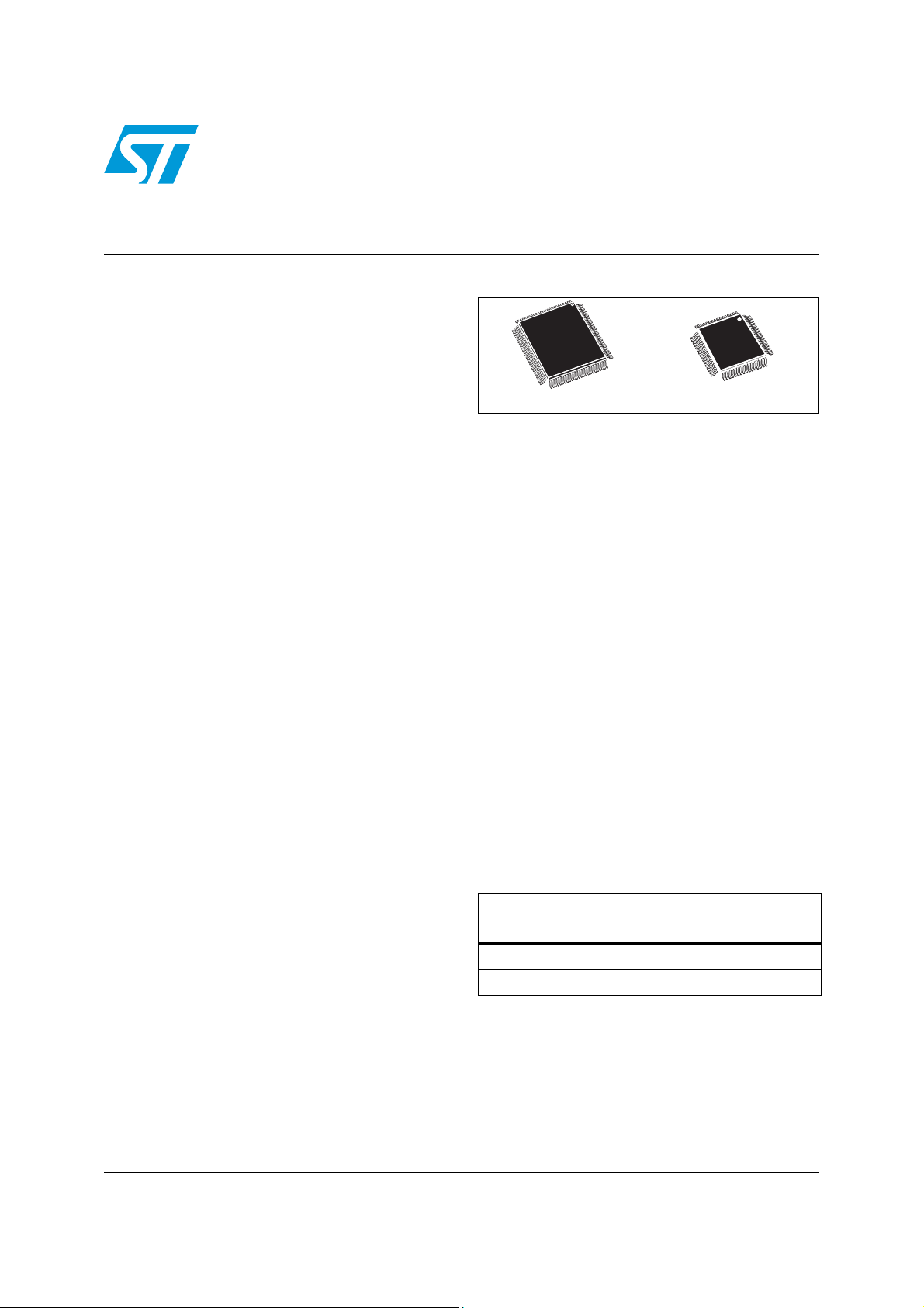
SPC560P34L1, SPC560P34L3
SPC560P40L1, SPC560P40L3
32-bit Power Architecture® based MCU with 320 KB Flash memory
and 20 KB RAM for automotive chassis and safety applications
Features
■ Up to 64 MHz, single issue, 32-bit CPU core
complex (e200z0h)
– Compliant with Power Architecture
embedded category
– Variable Length Encoding (VLE)
■ Memory organization
– Up to 256 KB on-chip code flash memory
with ECC and erase/program controller
– Additional 64 (4 × 16) KB on-chip data
flash memory with ECC for EEPROM
emulation
– Up to 20 KB on-chip SRAM with ECC
■ Fail-safe protection
– Programmable watchdog timer
– Non-maskable interrupt
– Fault collection unit
■ Nexus Class 1 interface
■ Interrupts and events
– 16-channel eDMA controller
– 16 priority level controller
– Up to 25 external interrupts
– PIT implements four 32-bit timers
– 120 interrupts are routed via INTC
■ 1 general purpose eTimer unit
– 6 timers each with up/down capabilities
– 16-bit resolution, cascadable counters
– Quadrature decode with rotation direction
flag
– Double buffer input capture and output
compare
■ GPIO (37 on LQFP64; 64 on LQFP100)
individually programmable as I/O or special
function
■ Communications interfaces
– 2 LINFlex channels (1× Master/Slave, 1×
Master only)
®
LQFP100 (14 x 14 x 1.4 mm)
– Up to 3 DSPI channels with automatic chip
LQFP64 (10 x 10 x 1.4 mm
select generation (up to 8/4/4 chip selects)
– Up to 2 FlexCAN interface (2.0B Active)
with 32 message buffers
– 1 safety port based on FlexCAN with 32
message buffers and up to 8 Mbit/s at
64 MHz capability usable as second CAN
when not used as safety port
■ One 10-bit analog-to-digital converter (ADC)
– Up to 16 input channels (16 on LQFP100 /
12 on LQFP64)
– Conversion time < 1 µs including sampling
time at full precision
– Programmable Cross Triggering Unit (CTU)
– 4 analog watchdogs with interrupt
capability
■ On-chip CAN/UART bootstrap loader with Boot
Assist Module (BAM)
■ 1 FlexPWM unit: 8 complementary or
independent outputs with ADC synchronization
signals
Table 1. Device summary
Package
LQFP100 SPC560P34L3 SPC560P40L3
LQFP64 SPC560P34L1 SPC560P40L1
192 Kbyte
Code Flash
256 Kbyte
Code Flash
December 2011 Doc ID 16100 Rev 5 1/103
www.st.com
1

Contents SPC560P34L1, SPC560P34L3, SPC560P40L1, SPC560P40L3
Contents
1 Introduction . . . . . . . . . . . . . . . . . . . . . . . . . . . . . . . . . . . . . . . . . . . . . . . . 7
1.1 Document overview . . . . . . . . . . . . . . . . . . . . . . . . . . . . . . . . . . . . . . . . . . 7
1.2 Description . . . . . . . . . . . . . . . . . . . . . . . . . . . . . . . . . . . . . . . . . . . . . . . . . 7
1.3 Device comparison . . . . . . . . . . . . . . . . . . . . . . . . . . . . . . . . . . . . . . . . . . . 7
1.4 Block diagram . . . . . . . . . . . . . . . . . . . . . . . . . . . . . . . . . . . . . . . . . . . . . . . 9
1.5 Feature details . . . . . . . . . . . . . . . . . . . . . . . . . . . . . . . . . . . . . . . . . . . . . 13
1.5.1 High performance e200z0 core processor . . . . . . . . . . . . . . . . . . . . . . . 13
1.5.2 Crossbar switch (XBAR) . . . . . . . . . . . . . . . . . . . . . . . . . . . . . . . . . . . . 13
1.5.3 Enhanced direct memory access (eDMA) . . . . . . . . . . . . . . . . . . . . . . . 14
1.5.4 Flash memory . . . . . . . . . . . . . . . . . . . . . . . . . . . . . . . . . . . . . . . . . . . . 14
1.5.5 Static random access memory (SRAM) . . . . . . . . . . . . . . . . . . . . . . . . . 15
1.5.6 Interrupt controller (INTC) . . . . . . . . . . . . . . . . . . . . . . . . . . . . . . . . . . . 16
1.5.7 System status and configuration module (SSCM) . . . . . . . . . . . . . . . . . 16
1.5.8 System clocks and clock generation . . . . . . . . . . . . . . . . . . . . . . . . . . . 17
1.5.9 Frequency-modulated phase-locked loop (FMPLL) . . . . . . . . . . . . . . . . 17
1.5.10 Main oscillator . . . . . . . . . . . . . . . . . . . . . . . . . . . . . . . . . . . . . . . . . . . . 17
1.5.11 Internal RC oscillator . . . . . . . . . . . . . . . . . . . . . . . . . . . . . . . . . . . . . . . 17
1.5.12 Periodic interrupt timer (PIT) . . . . . . . . . . . . . . . . . . . . . . . . . . . . . . . . . 18
1.5.13 System timer module (STM) . . . . . . . . . . . . . . . . . . . . . . . . . . . . . . . . . 18
1.5.14 Software watchdog timer (SWT) . . . . . . . . . . . . . . . . . . . . . . . . . . . . . . 18
1.5.15 Fault collection unit (FCU) . . . . . . . . . . . . . . . . . . . . . . . . . . . . . . . . . . . 18
1.5.16 System integration unit – Lite (SIUL) . . . . . . . . . . . . . . . . . . . . . . . . . . . 19
1.5.17 Boot and censorship . . . . . . . . . . . . . . . . . . . . . . . . . . . . . . . . . . . . . . . 19
1.5.18 Error correction status module (ECSM) . . . . . . . . . . . . . . . . . . . . . . . . . 19
1.5.19 Peripheral bridge (PBRIDGE) . . . . . . . . . . . . . . . . . . . . . . . . . . . . . . . . 20
1.5.20 Controller area network (FlexCAN) . . . . . . . . . . . . . . . . . . . . . . . . . . . . 20
1.5.21 Safety port (FlexCAN) . . . . . . . . . . . . . . . . . . . . . . . . . . . . . . . . . . . . . . 21
1.5.22 Serial communication interface module (LINFlex) . . . . . . . . . . . . . . . . . 22
1.5.23 Deserial serial peripheral interface (DSPI) . . . . . . . . . . . . . . . . . . . . . . 22
1.5.24 Pulse width modulator (FlexPWM) . . . . . . . . . . . . . . . . . . . . . . . . . . . . . 23
1.5.25 eTimer . . . . . . . . . . . . . . . . . . . . . . . . . . . . . . . . . . . . . . . . . . . . . . . . . . 25
1.5.26 Analog-to-digital converter (ADC) module . . . . . . . . . . . . . . . . . . . . . . . 25
1.5.27 Cross triggering unit (CTU) . . . . . . . . . . . . . . . . . . . . . . . . . . . . . . . . . . 26
1.5.28 Nexus Development Interface (NDI) . . . . . . . . . . . . . . . . . . . . . . . . . . . 26
2/103 Doc ID 16100 Rev 5

SPC560P34L1, SPC560P34L3, SPC560P40L1, SPC560P40L3 Contents
1.5.29 Cyclic redundancy check (CRC) . . . . . . . . . . . . . . . . . . . . . . . . . . . . . . 27
1.5.30 IEEE 1149.1 JTAG controller . . . . . . . . . . . . . . . . . . . . . . . . . . . . . . . . . 27
1.5.31 On-chip voltage regulator (VREG) . . . . . . . . . . . . . . . . . . . . . . . . . . . . . 28
2 Package pinouts and signal descriptions . . . . . . . . . . . . . . . . . . . . . . . 29
2.1 Package pinouts . . . . . . . . . . . . . . . . . . . . . . . . . . . . . . . . . . . . . . . . . . . . 29
2.2 Pin description . . . . . . . . . . . . . . . . . . . . . . . . . . . . . . . . . . . . . . . . . . . . . 32
2.2.1 Power supply and reference voltage pins . . . . . . . . . . . . . . . . . . . . . . . 32
2.2.2 System pins . . . . . . . . . . . . . . . . . . . . . . . . . . . . . . . . . . . . . . . . . . . . . . 34
2.2.3 Pin multiplexing . . . . . . . . . . . . . . . . . . . . . . . . . . . . . . . . . . . . . . . . . . . 34
3 Electrical characteristics . . . . . . . . . . . . . . . . . . . . . . . . . . . . . . . . . . . . 45
3.1 Introduction . . . . . . . . . . . . . . . . . . . . . . . . . . . . . . . . . . . . . . . . . . . . . . . 45
3.2 Parameter classification . . . . . . . . . . . . . . . . . . . . . . . . . . . . . . . . . . . . . . 45
3.3 Absolute maximum ratings . . . . . . . . . . . . . . . . . . . . . . . . . . . . . . . . . . . . 46
3.4 Recommended operating conditions . . . . . . . . . . . . . . . . . . . . . . . . . . . . 48
3.5 Thermal characteristics . . . . . . . . . . . . . . . . . . . . . . . . . . . . . . . . . . . . . . 52
3.5.1 Package thermal characteristics . . . . . . . . . . . . . . . . . . . . . . . . . . . . . . 52
3.5.2 General notes for specifications at maximum junction temperature . . . 52
3.6 Electromagnetic interference (EMI) characteristics . . . . . . . . . . . . . . . . . 54
3.7 Electrostatic discharge (ESD) characteristics . . . . . . . . . . . . . . . . . . . . . 54
3.8 Power management electrical characteristics . . . . . . . . . . . . . . . . . . . . . 54
3.8.1 Voltage regulator electrical characteristics . . . . . . . . . . . . . . . . . . . . . . 54
3.8.2 Voltage monitor electrical characteristics . . . . . . . . . . . . . . . . . . . . . . . . 56
3.9 Power up/down sequencing . . . . . . . . . . . . . . . . . . . . . . . . . . . . . . . . . . . 57
3.10 DC electrical characteristics . . . . . . . . . . . . . . . . . . . . . . . . . . . . . . . . . . . 59
3.10.1 NVUSRO register . . . . . . . . . . . . . . . . . . . . . . . . . . . . . . . . . . . . . . . . . . 59
3.10.2 DC electrical characteristics (5 V) . . . . . . . . . . . . . . . . . . . . . . . . . . . . . 60
3.10.3 DC electrical characteristics (3.3 V) . . . . . . . . . . . . . . . . . . . . . . . . . . . . 61
3.10.4 Input DC electrical characteristics definition . . . . . . . . . . . . . . . . . . . . . 63
3.10.5 I/O pad current specification . . . . . . . . . . . . . . . . . . . . . . . . . . . . . . . . . 63
3.11 Main oscillator electrical characteristics . . . . . . . . . . . . . . . . . . . . . . . . . . 64
3.12 FMPLL electrical characteristics . . . . . . . . . . . . . . . . . . . . . . . . . . . . . . . 66
3.13 16 MHz RC oscillator electrical characteristics . . . . . . . . . . . . . . . . . . . . 67
3.14 Analog-to-digital converter (ADC) electrical characteristics . . . . . . . . . . . 67
Doc ID 16100 Rev 5 3/103

Contents SPC560P34L1, SPC560P34L3, SPC560P40L1, SPC560P40L3
3.14.1 Input impedance and ADC accuracy . . . . . . . . . . . . . . . . . . . . . . . . . . . 68
3.14.2 ADC conversion characteristics . . . . . . . . . . . . . . . . . . . . . . . . . . . . . . . 72
3.15 Flash memory electrical characteristics . . . . . . . . . . . . . . . . . . . . . . . . . . 73
3.15.1 Program/Erase characteristics . . . . . . . . . . . . . . . . . . . . . . . . . . . . . . . . 73
3.15.2 Flash memory power supply DC characteristics . . . . . . . . . . . . . . . . . . 75
3.15.3 Start-up/Switch-off timings . . . . . . . . . . . . . . . . . . . . . . . . . . . . . . . . . . . 75
3.16 AC specifications . . . . . . . . . . . . . . . . . . . . . . . . . . . . . . . . . . . . . . . . . . . 76
3.16.1 Pad AC specifications . . . . . . . . . . . . . . . . . . . . . . . . . . . . . . . . . . . . . . 76
3.17 AC timing characteristics . . . . . . . . . . . . . . . . . . . . . . . . . . . . . . . . . . . . . 77
3.17.1 RESET pin characteristics . . . . . . . . . . . . . . . . . . . . . . . . . . . . . . . . . . . 77
3.17.2 IEEE 1149.1 interface timing . . . . . . . . . . . . . . . . . . . . . . . . . . . . . . . . . 80
3.17.3 Nexus timing . . . . . . . . . . . . . . . . . . . . . . . . . . . . . . . . . . . . . . . . . . . . . 82
3.17.4 External interrupt timing (IRQ pin) . . . . . . . . . . . . . . . . . . . . . . . . . . . . . 84
3.17.5 DSPI timing . . . . . . . . . . . . . . . . . . . . . . . . . . . . . . . . . . . . . . . . . . . . . . 85
4 Package characteristics . . . . . . . . . . . . . . . . . . . . . . . . . . . . . . . . . . . . . 91
4.1 ECOPACK® . . . . . . . . . . . . . . . . . . . . . . . . . . . . . . . . . . . . . . . . . . . . . . . 91
4.2 Package mechanical data . . . . . . . . . . . . . . . . . . . . . . . . . . . . . . . . . . . . 92
4.2.1 LQFP100 mechanical outline drawing . . . . . . . . . . . . . . . . . . . . . . . . . . 92
4.2.2 LQFP64 mechanical outline drawing . . . . . . . . . . . . . . . . . . . . . . . . . . . 94
5 Ordering information . . . . . . . . . . . . . . . . . . . . . . . . . . . . . . . . . . . . . . . 96
Appendix A Abbreviations. . . . . . . . . . . . . . . . . . . . . . . . . . . . . . . . . . . . . . . . . . . 97
Revision history . . . . . . . . . . . . . . . . . . . . . . . . . . . . . . . . . . . . . . . . . . . . . . . . . . . . 98
4/103 Doc ID 16100 Rev 5

SPC560P34L1, SPC560P34L3, SPC560P40L1, SPC560P40L3 List of tables
List of tables
Table 1. Device summary . . . . . . . . . . . . . . . . . . . . . . . . . . . . . . . . . . . . . . . . . . . . . . . . . . . . . . . . . . 1
Table 2. SPC560P34/SPC560P40 device comparison . . . . . . . . . . . . . . . . . . . . . . . . . . . . . . . . . . . 7
Table 3. SPC560P40 device configuration differences . . . . . . . . . . . . . . . . . . . . . . . . . . . . . . . . . . . 9
Table 4. SPC560P34/SPC560P40 series block summary . . . . . . . . . . . . . . . . . . . . . . . . . . . . . . . . 11
Table 5. Supply pins . . . . . . . . . . . . . . . . . . . . . . . . . . . . . . . . . . . . . . . . . . . . . . . . . . . . . . . . . . . . . 33
Table 6. System pins . . . . . . . . . . . . . . . . . . . . . . . . . . . . . . . . . . . . . . . . . . . . . . . . . . . . . . . . . . . . 34
Table 7. Pin muxing . . . . . . . . . . . . . . . . . . . . . . . . . . . . . . . . . . . . . . . . . . . . . . . . . . . . . . . . . . . . . 35
Table 8. Parameter classifications . . . . . . . . . . . . . . . . . . . . . . . . . . . . . . . . . . . . . . . . . . . . . . . . . . 45
Table 9. Absolute maximum ratings . . . . . . . . . . . . . . . . . . . . . . . . . . . . . . . . . . . . . . . . . . . . . . . . . 46
Table 10. Recommended operating conditions (5.0 V) . . . . . . . . . . . . . . . . . . . . . . . . . . . . . . . . . . . 48
Table 11. Recommended operating conditions (3.3 V) . . . . . . . . . . . . . . . . . . . . . . . . . . . . . . . . . . . 49
Table 12. LQFP thermal characteristics . . . . . . . . . . . . . . . . . . . . . . . . . . . . . . . . . . . . . . . . . . . . . . . 52
Table 13. EMI testing specifications . . . . . . . . . . . . . . . . . . . . . . . . . . . . . . . . . . . . . . . . . . . . . . . . . . 54
Table 14. ESD ratings, . . . . . . . . . . . . . . . . . . . . . . . . . . . . . . . . . . . . . . . . . . . . . . . . . . . . . . . . . . . . 54
Table 15. Approved NPN ballast components . . . . . . . . . . . . . . . . . . . . . . . . . . . . . . . . . . . . . . . . . . 55
Table 16. Voltage regulator electrical characteristics . . . . . . . . . . . . . . . . . . . . . . . . . . . . . . . . . . . . . 56
Table 17. Low voltage monitor electrical characteristics. . . . . . . . . . . . . . . . . . . . . . . . . . . . . . . . . . . 57
Table 18. PAD3V5V field description . . . . . . . . . . . . . . . . . . . . . . . . . . . . . . . . . . . . . . . . . . . . . . . . . 59
Table 19. DC electrical characteristics (5.0 V, NVUSRO[PAD3V5V] = 0) . . . . . . . . . . . . . . . . . . . . . 60
Table 20. Supply current (5.0 V, NVUSRO[PAD3V5V] = 0) . . . . . . . . . . . . . . . . . . . . . . . . . . . . . . . . 61
Table 21. DC electrical characteristics (3.3 V, NVUSRO[PAD3V5V] = 1) . . . . . . . . . . . . . . . . . . . . . 61
Table 22. Supply current (3.3 V, NVUSRO[PAD3V5V] = 1) . . . . . . . . . . . . . . . . . . . . . . . . . . . . . . . . 62
Table 23. I/O supply segment. . . . . . . . . . . . . . . . . . . . . . . . . . . . . . . . . . . . . . . . . . . . . . . . . . . . . . . 63
Table 24. I/O consumption . . . . . . . . . . . . . . . . . . . . . . . . . . . . . . . . . . . . . . . . . . . . . . . . . . . . . . . . . 63
Table 25. Main oscillator output electrical characteristics (5.0 V, NVUSRO[PAD3V5V] = 0) . . . . . . . 65
Table 26. Main oscillator output electrical characteristics (3.3 V, NVUSRO[PAD3V5V] = 1) . . . . . . . 65
Table 27. Input clock characteristics. . . . . . . . . . . . . . . . . . . . . . . . . . . . . . . . . . . . . . . . . . . . . . . . . . 66
Table 28. FMPLL electrical characteristics . . . . . . . . . . . . . . . . . . . . . . . . . . . . . . . . . . . . . . . . . . . . . 66
Table 29. 16 MHz RC oscillator electrical characteristics . . . . . . . . . . . . . . . . . . . . . . . . . . . . . . . . . . 67
Table 30. ADC conversion characteristics . . . . . . . . . . . . . . . . . . . . . . . . . . . . . . . . . . . . . . . . . . . . . 72
Table 31. Program and erase specifications . . . . . . . . . . . . . . . . . . . . . . . . . . . . . . . . . . . . . . . . . . . 73
Table 32. Flash memory module life. . . . . . . . . . . . . . . . . . . . . . . . . . . . . . . . . . . . . . . . . . . . . . . . . . 74
Table 33. Flash memory read access timing . . . . . . . . . . . . . . . . . . . . . . . . . . . . . . . . . . . . . . . . . . . 74
Table 34. Flash memory power supply DC electrical characteristics . . . . . . . . . . . . . . . . . . . . . . . . . 75
Table 35. Start-up time/Switch-off time. . . . . . . . . . . . . . . . . . . . . . . . . . . . . . . . . . . . . . . . . . . . . . . . 75
Table 36. Output pin transition times . . . . . . . . . . . . . . . . . . . . . . . . . . . . . . . . . . . . . . . . . . . . . . . . . 76
Table 37. RESET electrical characteristics. . . . . . . . . . . . . . . . . . . . . . . . . . . . . . . . . . . . . . . . . . . . . 78
Table 38. JTAG pin AC electrical characteristics . . . . . . . . . . . . . . . . . . . . . . . . . . . . . . . . . . . . . . . . 80
Table 39. Nexus debug port timing . . . . . . . . . . . . . . . . . . . . . . . . . . . . . . . . . . . . . . . . . . . . . . . . . . . 82
Table 40. External interrupt timing . . . . . . . . . . . . . . . . . . . . . . . . . . . . . . . . . . . . . . . . . . . . . . . . . . . 84
Table 41. DSPI timing . . . . . . . . . . . . . . . . . . . . . . . . . . . . . . . . . . . . . . . . . . . . . . . . . . . . . . . . . . . . . 85
Table 42. LQFP100 package mechanical data. . . . . . . . . . . . . . . . . . . . . . . . . . . . . . . . . . . . . . . . . . 93
Table 43. LQFP64 package mechanical data. . . . . . . . . . . . . . . . . . . . . . . . . . . . . . . . . . . . . . . . . . . 94
Table 44. Abbreviations . . . . . . . . . . . . . . . . . . . . . . . . . . . . . . . . . . . . . . . . . . . . . . . . . . . . . . . . . . . 97
Doc ID 16100 Rev 5 5/103

List of figures SPC560P34L1, SPC560P34L3, SPC560P40L1, SPC560P40L3
List of figures
Figure 1. Block diagram (SPC560P40 full-featured configuration) . . . . . . . . . . . . . . . . . . . . . . . . . . 10
Figure 2. 64-pin LQFP pinout – Full featured configuration (top view) . . . . . . . . . . . . . . . . . . . . . . . 29
Figure 3. 64-pin LQFP pinout – airbag configuration (top view) . . . . . . . . . . . . . . . . . . . . . . . . . . . . 30
Figure 4. 100-pin LQFP pinout – full featured configuration (top view) . . . . . . . . . . . . . . . . . . . . . . . 31
Figure 5. 100-pin LQFP pinout – airbag configuration (top view) . . . . . . . . . . . . . . . . . . . . . . . . . . . 32
Figure 6. Power supplies constraints (–0.3 V ≤ V
Figure 7. Independent ADC supply (–0.3 V ≤ V
Figure 8. Power supplies constraints (3.0 V ≤ V
Figure 9. Independent ADC supply (3.0 V ≤ V
DD_HV_IOx
DD_HV_REG
DD_HV_IOx
DD_HV_REG
Figure 10. Voltage regulator configuration . . . . . . . . . . . . . . . . . . . . . . . . . . . . . . . . . . . . . . . . . . . . . . 55
Figure 11. Power-up typical sequence. . . . . . . . . . . . . . . . . . . . . . . . . . . . . . . . . . . . . . . . . . . . . . . . . 58
Figure 12. Power-down typical sequence . . . . . . . . . . . . . . . . . . . . . . . . . . . . . . . . . . . . . . . . . . . . . . 58
Figure 13. Brown-out typical sequence . . . . . . . . . . . . . . . . . . . . . . . . . . . . . . . . . . . . . . . . . . . . . . . . 59
Figure 14. Input DC electrical characteristics definition . . . . . . . . . . . . . . . . . . . . . . . . . . . . . . . . . . . . 63
Figure 15. ADC characteristics and error definitions . . . . . . . . . . . . . . . . . . . . . . . . . . . . . . . . . . . . . . 68
Figure 16. Input equivalent circuit . . . . . . . . . . . . . . . . . . . . . . . . . . . . . . . . . . . . . . . . . . . . . . . . . . . . 69
Figure 17. Transient behavior during sampling phase . . . . . . . . . . . . . . . . . . . . . . . . . . . . . . . . . . . . . 70
Figure 18. Spectral representation of input signal . . . . . . . . . . . . . . . . . . . . . . . . . . . . . . . . . . . . . . . . 71
Figure 19. Pad output delay . . . . . . . . . . . . . . . . . . . . . . . . . . . . . . . . . . . . . . . . . . . . . . . . . . . . . . . . . 77
Figure 20. Start-up reset requirements . . . . . . . . . . . . . . . . . . . . . . . . . . . . . . . . . . . . . . . . . . . . . . . . 77
Figure 21. Noise filtering on reset signal . . . . . . . . . . . . . . . . . . . . . . . . . . . . . . . . . . . . . . . . . . . . . . . 78
Figure 22. JTAG test clock input timing . . . . . . . . . . . . . . . . . . . . . . . . . . . . . . . . . . . . . . . . . . . . . . . . 80
Figure 23. JTAG test access port timing . . . . . . . . . . . . . . . . . . . . . . . . . . . . . . . . . . . . . . . . . . . . . . . 81
Figure 24. JTAG boundary scan timing . . . . . . . . . . . . . . . . . . . . . . . . . . . . . . . . . . . . . . . . . . . . . . . . 82
Figure 25. Nexus output timing . . . . . . . . . . . . . . . . . . . . . . . . . . . . . . . . . . . . . . . . . . . . . . . . . . . . . . 83
Figure 26. Nexus event trigger and test clock timing . . . . . . . . . . . . . . . . . . . . . . . . . . . . . . . . . . . . . . 83
Figure 27. Nexus TDI, TMS, TDO timing . . . . . . . . . . . . . . . . . . . . . . . . . . . . . . . . . . . . . . . . . . . . . . . 84
Figure 28. External interrupt timing . . . . . . . . . . . . . . . . . . . . . . . . . . . . . . . . . . . . . . . . . . . . . . . . . . . 85
Figure 29. DSPI classic SPI timing – Master, CPHA = 0 . . . . . . . . . . . . . . . . . . . . . . . . . . . . . . . . . . . 86
Figure 30. DSPI classic SPI timing – Master, CPHA = 1 . . . . . . . . . . . . . . . . . . . . . . . . . . . . . . . . . . . 87
Figure 31. DSPI classic SPI timing – Slave, CPHA = 0 . . . . . . . . . . . . . . . . . . . . . . . . . . . . . . . . . . . . 87
Figure 32. DSPI classic SPI timing – Slave, CPHA = 1 . . . . . . . . . . . . . . . . . . . . . . . . . . . . . . . . . . . . 88
Figure 33. DSPI modified transfer format timing – Master, CPHA = 0. . . . . . . . . . . . . . . . . . . . . . . . . 88
Figure 34. DSPI modified transfer format timing – Master, CPHA = 1. . . . . . . . . . . . . . . . . . . . . . . . . 89
Figure 35. DSPI modified transfer format timing – Slave, CPHA = 0. . . . . . . . . . . . . . . . . . . . . . . . . . 89
Figure 36. DSPI modified transfer format timing – Slave, CPHA = 1. . . . . . . . . . . . . . . . . . . . . . . . . . 90
Figure 37. DSPI PCS Strobe (PCSS) timing . . . . . . . . . . . . . . . . . . . . . . . . . . . . . . . . . . . . . . . . . . . . 90
Figure 38. LQFP100 package mechanical drawing . . . . . . . . . . . . . . . . . . . . . . . . . . . . . . . . . . . . . . . 92
Figure 39. LQFP64 package mechanical drawing . . . . . . . . . . . . . . . . . . . . . . . . . . . . . . . . . . . . . . . . 94
Figure 40. Commercial product code structure . . . . . . . . . . . . . . . . . . . . . . . . . . . . . . . . . . . . . . . . . . 96
≤ 6.0 V). . . . . . . . . . . . . . . . . . . . . . . . . 47
≤ 6.0 V) . . . . . . . . . . . . . . . . . . . . . . . . . 48
≤ 5.5 V). . . . . . . . . . . . . . . . . . . . . . . . . . 51
≤ 5.5 V) . . . . . . . . . . . . . . . . . . . . . . . . . . 51
6/103 Doc ID 16100 Rev 5

SPC560P34L1, SPC560P34L3, SPC560P40L1, SPC560P40L3 Introduction
1 Introduction
1.1 Document overview
This document provides electrical specifications, pin assignments, and package diagrams
for the SPC560P34/40 series of microcontroller units (MCUs). It also describes the device
features and highlights important electrical and physical characteristics. For functional
characteristics, refer to the device reference manual.
1.2 Description
This 32-bit system-on-chip (SoC) automotive microcontroller family is the latest achievement
in integrated automotive application controllers. It belongs to an expanding range of
automotive-focused products designed to address chassis applications—specifically,
electrical hydraulic power steering (EHPS) and electric power steering (EPS)—as well as
airbag applications.
This family is one of a series of next-generation integrated automotive microcontrollers
based on the Power Architecture technology.
The advanced and cost-efficient host processor core of this automotive controller family
complies with the Power Architecture embedded category. It operates at speeds of up to
64 MHz and offers high performance processing optimized for low power consumption. It
capitalizes on the available development infrastructure of current Power Architecture
devices and is supported with software drivers, operating systems and configuration code to
assist with users implementations.
1.3 Device comparison
Ta bl e 2
and their features—relative to full-featured version—to enable a comparison among the
family members and an understanding of the range of functionality offered within this family.
Table 2. SPC560P34/SPC560P40 device comparison
provides a summary of different members of the SPC560P34/SPC560P40 family
Feature
Code flash memory (with ECC) 192 KB 256 KB
Data flash memory / EE option (with ECC) 64 KB
SRAM (with ECC) 12 KB 20 KB
Processor core 32-bit e200z0h
Instruction set VLE (variable length encoding)
CPU performance 0–64 MHz
FMPLL (frequency-modulated phase-locked loop)
module
INTC (interrupt controller) channels 120
PIT (periodic interrupt timer) 1 (with four 32-bit timers)
SPC560P34 SPC560P40
Full-featured
1
Doc ID 16100 Rev 5 7/103

Introduction SPC560P34L1, SPC560P34L3, SPC560P40L1, SPC560P40L3
Table 2. SPC560P34/SPC560P40 device comparison (continued)
Feature
eDMA (enhanced direct memory access)
channels
FlexCAN (controller area network) 1
Safety port No
SPC560P34 SPC560P40
Full-featured
16
(1)
(1),(2)
2
Yes (via second
FlexCAN module)
FCU (fault collection unit) Yes
CTU (cross triggering unit) Yes Yes
eTimer 1 (16-bit, 6 channels)
FlexPWM (pulse-width modulation) channels
8
(capture capabity not
supported)
(capture capability not
8
supported)
Analog-to-digital converter (ADC) 1 (10-bit, 16 channels)
LINFlex
2
(1 × Master/Slave,
1 × Master only)
(1 × Master/Slave,
2
1 × Master only)
DSPI (deserial serial peripheral interface) 2 3
CRC (cyclic redundancy check) unit Yes
Junction temperature sensor No
JTAG controller Yes
Nexus port controller (NPC) Yes (Nexus Class 1)
Digital power supply
(3)
3.3 V or 5 V single supply with external transistor
Analog power supply 3.3 V or 5 V
Supply
Internal RC oscillator 16 MHz
External crystal oscillator 4–40 MHz
Packages
LQFP64
LQFP100
Temperature Standard ambient temperature –40 to 125 °C
1. Each FlexCAN module has 32 message buffers.
2. One FlexCAN module can act as a safety port with a bit rate as high as 8 Mbit/s at 64 MHz.
3. The different supply voltages vary according to the part number ordered.
SPC560P34/SPC560P40 is available in two configurations having different features: Fullfeatured and airbag.
Ta bl e 3
shows the main differences between the two versions of the
SPC560P40 MCU.
8/103 Doc ID 16100 Rev 5

SPC560P34L1, SPC560P34L3, SPC560P40L1, SPC560P40L3 Introduction
Table 3.
SRAM (with ECC) 16 KB 20 KB
FlexCAN (controller area network) 1 2
Safety port No
FlexPWM (pulse-width modulation) channels No
CTU (cross triggering unit) No Yes
SPC560P40 device configuration differences
Feature
Configuration
Airbag Full-featured
Ye s
(via second FlexCAN module)
8
(capture capability not
supported)
1.4 Block diagram
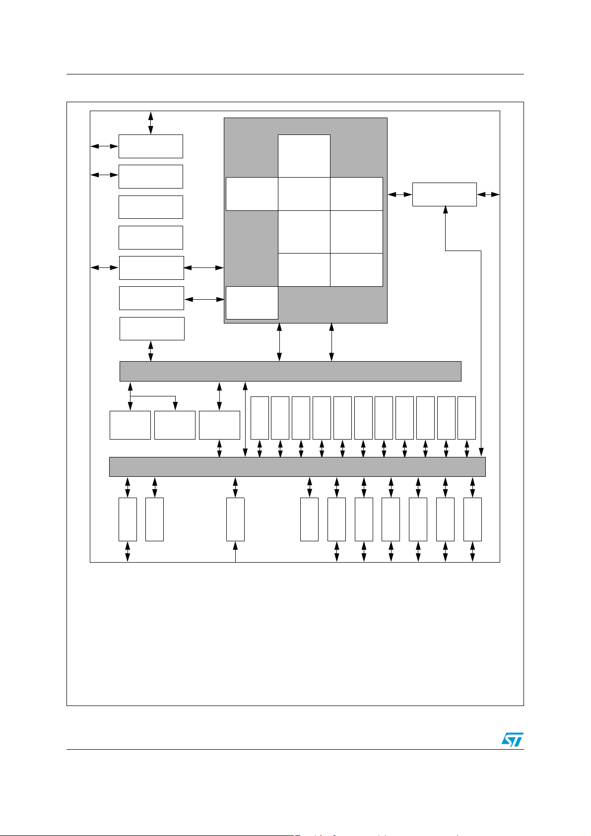
Figure 1
summarizes the functions of the blocks.
shows a top-level block diagram of the SPC560P34/SPC560P40 MCU.
Ta bl e 4
Doc ID 16100 Rev 5 9/103
Introduction SPC560P34L1, SPC560P34L3, SPC560P40L1, SPC560P40L3
Figure 1. Block diagram (SPC560P40 full-featured configuration)
External ballast
1.2 V regulator
control
XOSC
16 MHz
RC oscillator
FMPLL_0
(System)
JTAG
Nexus port
controller
eDMA
eDMA
16 channels
16 channels
Master
e200z0 Core
32-bit
general
purpose
registers
Integer
execu tion
unit
Nexus 1
Instruction
32-bit
Master
Crossbar switch (XBAR, AMBA 2.0 v6 AHB)
Slave SlaveSlave
Special
purpose
registers
Instruction
unit
Branch
prediction
unit
Exception
handler
Var iable
length
encoded
instructions
Load/store
unit
Data
32-bit
Master
Interrupt
controller
Code Flash
(with ECC)
Legend:
ADC Analog-to-digital converter
BAM Boot assist module
CRC Cyclic redundancy check
CTU Cross triggering unit
DSPI Deserial serial peripheral interface
ECSM Error correction status module
eDMA Enhanced direct memory access
eTimer Enhanced timer
FCU Fault collection unit
Flash Flash memory
FlexCAN Controller area network
FlexPWM Flexible pulse width modulation
FMPLL Frequency-modulated phase-locked loop
INTC Interrupt controller
JTAG JTAG controller
Data Flash
(with ECC)
CTU
FlexPWM
SRAM
(with ECC)
ADC
(10 bit, 16 ch)
PIT
WKPU
Peripheral bridge
STM
CRC
SSCM
LINFlex Serial communication interface (LIN support)
MC_CGM Clock generation module
MC_ME Mode entry module
MC_PCU Power control unit
MC_RGM Reset generation module
PIT Periodic interrupt timer
SIUL System Integration unit Lite
SRAM Static random-access memory
SSCM System status and configuration module
STM System timer module
SWT Software watchdog timer
WKPU Wakeup unit
XOSC External oscillator
XBAR Crossbar switch
SWT
MC_RGM
3×
eTimer
DSPI
(6 ch)
MC_CGM
2×
MC_ME
LINFlex
SIUL
BAM
FlexCAN
Safety port
ECSM
FCU
10/103 Doc ID 16100 Rev 5

SPC560P34L1, SPC560P34L3, SPC560P40L1, SPC560P40L3 Introduction
Table 4. SPC560P34/SPC560P40 series block summary
Block Function
Analog-to-digital converter (ADC) Multi-channel, 10-bit analog-to-digital converter
Boot assist module (BAM)
Clock generation module
(MC_CGM)
Controller area network
(FlexCAN)
Cross triggering unit (CTU)
Crossbar switch (XBAR)
Block of read-only memory containing VLE code which is executed according to
the boot mode of the device
Provides logic and control required for the generation of system and peripheral
clocks
Supports the standard CAN communications protocol
Enables synchronization of ADC conversions with a timer event from the eMIOS
or from the PIT
Supports simultaneous connections between two master ports and three slave
ports; supports a 32-bit address bus width and a 32-bit data bus width
Cyclic redundancy check (CRC) CRC checksum generator
Deserial serial peripheral
interface (DSPI)
Enhanced direct memory access
(eDMA)
Provides a synchronous serial interface for communication with external
devices
Performs complex data transfers with minimal intervention from a host
processor via “
n
” programmable channels
Enhanced timer (eTimer) Provides enhanced programmable up/down modulo counting
Provides a myriad of miscellaneous control functions for the device including
Error correction status module
(ECSM)
program-visible information about configuration and revision levels, a reset
status register, wakeup control for exiting sleep modes, and optional features
such as information on memory errors reported by error-correcting codes
External oscillator (XOSC)
Provides an output clock used as input reference for FMPLL_0 or as reference
clock for specific modules depending on system needs
Fault collection unit (FCU) Provides functional safety to the device
Flash memory Provides non-volatile storage for program code, constants and variables
Frequency-modulated phaselocked loop (FMPLL)
Generates high-speed system clocks and supports programmable frequency
modulation
Interrupt controller (INTC) Provides priority-based preemptive scheduling of interrupt requests
JTAG controller
LINFlex controller
Provides the means to test chip functionality and connectivity while remaining
transparent to system logic when not in test mode
Manages a high number of LIN (Local Interconnect Network protocol)
messages efficiently with a minimum of CPU load
Provides a mechanism for controlling the device operational mode and mode
Mode entry module (MC_ME)
transition sequences in all functional states; also manages the power control
unit, reset generation module and clock generation module, and holds the
configuration, control and status registers accessible for applications
Periodic interrupt timer (PIT) Produces periodic interrupts and triggers
Peripheral bridge (PBRIDGE) Is the interface between the system bus and on-chip peripherals
Power control unit (MC_PCU)
Reduces the overall power consumption by disconnecting parts of the device
from the power supply via a power switching device; device components are
grouped into sections called “power domains” which are controlled by the PCU
Doc ID 16100 Rev 5 11/103

Introduction SPC560P34L1, SPC560P34L3, SPC560P40L1, SPC560P40L3
Table 4. SPC560P34/SPC560P40 series block summary (continued)
Block Function
Pulse width modulator
(FlexPWM)
Reset generation module
(MC_RGM)
Static random-access memory
(SRAM)
Contains four PWM submodules, each of which capable of controlling a single
half-bridge power stage and two fault input channels
Centralizes reset sources and manages the device reset sequence of the
device
Provides storage for program code, constants, and variables
Provides control over all the electrical pad controls and up 32 ports with 16 bits
System integration unit lite (SIUL)
of bidirectional, general-purpose input and output signals and supports up to 32
external interrupts with trigger event configuration
System status and configuration
module (SSCM)
System timer module (STM)
Provides system configuration and status data (such as memory size and
status, device mode and security status), device identification data, debug
status port enable and selection, and bus and peripheral abort enable/disable
Provides a set of output compare events to support AUTOSAR
system tasks
System watchdog timer (SWT) Provides protection from runaway code
Supports up to 18 external sources that can generate interrupts or wakeup
Wakeup unit (WKPU)
events, of which 1 can cause non-maskable interrupt requests or wakeup
events
1. AUTOSAR: AUTomotive Open System ARchitecture (see www.autosar.org)
(1)
and operating
12/103 Doc ID 16100 Rev 5

SPC560P34L1, SPC560P34L3, SPC560P40L1, SPC560P40L3 Introduction
1.5 Feature details
1.5.1 High performance e200z0 core processor
The e200z0 Power Architecture core provides the following features:
● High performance e200z0 core processor for managing peripherals and interrupts
● Single issue 4-stage pipeline in-order execution 32-bit Power Architecture CPU
● Harvard architecture
● Variable length encoding (VLE), allowing mixed 16- and 32-bit instructions
– Results in smaller code size footprint
– Minimizes impact on performance
● Branch processing acceleration using lookahead instruction buffer
● Load/store unit
– 1-cycle load latency
– Misaligned access support
– No load-to-use pipeline bubbles
● Thirty-two 32-bit general purpose registers (GPRs)
● Separate instruction bus and load/store bus Harvard architecture
● Hardware vectored interrupt support
● Reservation instructions for implementing read-modify-write constructs
● Long cycle time instructions, except for guarded loads, do not increase interrupt latency
● Extensive system development support through Nexus debug port
● Non-maskable interrupt support
1.5.2 Crossbar switch (XBAR)
The XBAR multi-port crossbar switch supports simultaneous connections between three
master ports and three slave ports. The crossbar supports a 32-bit address bus width and a
32-bit data bus width.
The crossbar allows for two concurrent transactions to occur from any master port to any
slave port; but one of those transfers must be an instruction fetch from internal flash
memory. If a slave port is simultaneously requested by more than one master port,
arbitration logic will select the higher priority master and grant it ownership of the slave port.
All other masters requesting that slave port will be stalled until the higher priority master
completes its transactions. Requesting masters will be treated with equal priority and will be
granted access a slave port in round-robin fashion, based upon the ID of the last master to
be granted access.
Doc ID 16100 Rev 5 13/103

Introduction SPC560P34L1, SPC560P34L3, SPC560P40L1, SPC560P40L3
The crossbar provides the following features:
● 3 master ports:
– e200z0 core complex instruction port
– e200z0 core complex Load/Store Data port
–eDMA
● 3 slave ports:
– Flash memory (Code and Data)
–SRAM
– Peripheral bridge
● 32-bit internal address, 32-bit internal data paths
● Fixed Priority Arbitration based on Port Master
● Temporary dynamic priority elevation of masters
1.5.3 Enhanced direct memory access (eDMA)
The enhanced direct memory access (eDMA) controller is a second-generation module
capable of performing complex data movements via 16 programmable channels, with
minimal intervention from the host processor. The hardware micro architecture includes a
DMA engine which performs source and destination address calculations, and the actual
data movement operations, along with an SRAM-based memory containing the transfer
control descriptors (TCD) for the channels.
The eDMA module provides the following features:
● 16 channels support independent 8-, 16- or 32-bit single value or block transfers
● Supports variable-sized queues and circular queues
● Source and destination address registers are independently configured to either post-
increment or to remain constant
● Each transfer is initiated by a peripheral, CPU, or eDMA channel request
● Each eDMA channel can optionally send an interrupt request to the CPU on completion
of a single value or block transfer
● DMA transfers possible between system memories, DSPIs, ADC, FlexPWM, eTimer
and CTU
● Programmable DMA channel multiplexer allows assignment of any DMA source to any
available DMA channel with as many as 30 request sources
● eDMA abort operation through software
1.5.4 Flash memory
The SPC560P34/SPC560P40 provides 320 KB of programmable, non-volatile, flash
memory. The non-volatile memory (NVM) can be used for instruction and/or data storage.
The flash memory module is interfaced to the system bus by a dedicated flash memory
controller. It supports a 32-bit data bus width at the system bus port, and a 128-bit read data
interface to flash memory. The module contains four 128-bit wide prefetch buffers. Prefetch
buffer hits allow no-wait responses. Normal flash memory array accesses are registered and
are forwarded to the system bus on the following cycle, incurring two wait-states.
14/103 Doc ID 16100 Rev 5

SPC560P34L1, SPC560P34L3, SPC560P40L1, SPC560P40L3 Introduction
The flash memory module provides the following features:
● As much as 320 KB flash memory
– 6 blocks (32 KB + 2×16 KB + 32 KB + 32 KB + 128 KB) code flash memory
– 4 blocks (16 KB + 16 KB + 16 KB + 16 KB) data flash memory
– Full Read-While-Write (RWW) capability between code flash memory and data
flash memory
● Four 128-bit wide prefetch buffers to provide single cycle in-line accesses (prefetch
buffers can be configured to prefetch code or data or both)
● Typical flash memory access time: no wait-state for buffer hits, 2 wait-states for page
buffer miss at 64 MHz
● Hardware managed flash memory writes handled by 32-bit RISC Krypton engine
● Hardware and software configurable read and write access protections on a per-master
basis
● Configurable access timing allowing use in a wide range of system frequencies
● Multiple-mapping support and mapping-based block access timing (up to 31 additional
cycles) allowing use for emulation of other memory types
● Software programmable block program/erase restriction control
● Erase of selected block(s)
● Read page sizes
– Code flash memory: 128 bits (4 words)
– Data flash memory: 32 bits (1 word)
● ECC with single-bit correction, double-bit detection for data integrity
– Code flash memory: 64-bit ECC
– Data flash memory: 32-bit ECC
● Embedded hardware program and erase algorithm
● Erase suspend and program abort
● Censorship protection scheme to prevent flash memory content visibility
● Hardware support for EEPROM emulation
1.5.5 Static random access memory (SRAM)
The SPC560P34/SPC560P40 SRAM module provides up to 20 KB of general-purpose
memory.
The SRAM module provides the following features:
● Supports read/write accesses mapped to the SRAM from any master
● Up to 20 KB general purpose SRAM
● Supports byte (8-bit), half word (16-bit), and word (32-bit) writes for optimal use of
memory
● Typical SRAM access time: no wait-state for reads and 32-bit writes; 1 wait-state for 8-
and 16-bit writes if back-to-back with a read to same memory block
Doc ID 16100 Rev 5 15/103

Introduction SPC560P34L1, SPC560P34L3, SPC560P40L1, SPC560P40L3
1.5.6 Interrupt controller (INTC)
The interrupt controller (INTC) provides priority-based preemptive scheduling of interrupt
requests, suitable for statically scheduled hard real-time systems. The INTC handles 128
selectable-priority interrupt sources.
For high-priority interrupt requests, the time from the assertion of the interrupt request by
the peripheral to the execution of the interrupt service routine (ISR) by the processor has
been minimized. The INTC provides a unique vector for each interrupt request source for
quick determination of which ISR has to be executed. It also provides a wide number of
priorities so that lower priority ISRs do not delay the execution of higher priority ISRs. To
allow the appropriate priorities for each source of interrupt request, the priority of each
interrupt request is software configurable.
When multiple tasks share a resource, coherent accesses to that resource need to be
supported. The INTC supports the priority ceiling protocol (PCP) for coherent accesses. By
providing a modifiable priority mask, the priority can be raised temporarily so that all tasks
which share the same resource can not preempt each other.
The INTC provides the following features:
● Unique 9-bit vector for each separate interrupt source
● 8 software triggerable interrupt sources
● 16 priority levels with fixed hardware arbitration within priority levels for each interrupt
source
● Ability to modify the ISR or task priority: modifying the priority can be used to
implement the priority ceiling protocol for accessing shared resources.
● 1 external high priority interrupt (NMI) directly accessing the main core and I/O
processor (IOP) critical interrupt mechanism
1.5.7 System status and configuration module (SSCM)
The system status and configuration module (SSCM) provides central device functionality.
The SSCM includes these features:
● System configuration and status
– Memory sizes/status
– Device mode and security status
– Determine boot vector
– Search code flash for bootable sector
– DMA status
● Debug status port enable and selection
● Bus and peripheral abort enable/disable
16/103 Doc ID 16100 Rev 5

SPC560P34L1, SPC560P34L3, SPC560P40L1, SPC560P40L3 Introduction
1.5.8 System clocks and clock generation
The following list summarizes the system clock and clock generation on the
SPC560P34/SPC560P40:
● Lock detect circuitry continuously monitors lock status
● Loss of clock (LOC) detection for PLL outputs
● Programmable output clock divider (÷1, ÷2, ÷4, ÷8)
● FlexPWM module and eTimer module running at the same frequency as the e200z0h
core
● Internal 16 MHz RC oscillator for rapid start-up and safe mode: supports frequency
trimming by user application
1.5.9 Frequency-modulated phase-locked loop (FMPLL)
The FMPLL allows the user to generate high speed system clocks from a 4–40 MHz input
clock. Further, the FMPLL supports programmable frequency modulation of the system
clock. The PLL multiplication factor, output clock divider ratio are all software configurable.
The FMPLL has the following major features:
● Input clock frequency: 4–40 MHz
● Maximum output frequency: 64 MHz
● Voltage controlled oscillator (VCO)—frequency 256–512 MHz
● Reduced frequency divider (RFD) for reduced frequency operation without forcing the
FMPLL to relock
● Frequency-modulated PLL
– Modulation enabled/disabled through software
– Triangle wave modulation
● Programmable modulation depth (±0.25% to ±4% deviation from center frequency):
programmable modulation frequency dependent on reference frequency
● Self-clocked mode (SCM) operation
1.5.10 Main oscillator
The main oscillator provides these features:
● Input frequency range: 4–40 MHz
● Crystal input mode or oscillator input mode
● PLL reference
1.5.11 Internal RC oscillator
This device has an RC ladder phase-shift oscillator. The architecture uses constant current
charging of a capacitor. The voltage at the capacitor is compared by the stable bandgap
reference voltage.
Doc ID 16100 Rev 5 17/103

Introduction SPC560P34L1, SPC560P34L3, SPC560P40L1, SPC560P40L3
The RC oscillator provides these features:
● Nominal frequency 16 MHz
● ±5 % variation over voltage and temperature after process trim
● Clock output of the RC oscillator serves as system clock source in case loss of lock or
loss of clock is detected by the PLL
● RC oscillator is used as the default system clock during startup
1.5.12 Periodic interrupt timer (PIT)
The PIT module implements these features:
● 4 general-purpose interrupt timers
● 32-bit counter resolution
● Clocked by system clock frequency
● Each channel usable as trigger for a DMA request
1.5.13 System timer module (STM)
The STM implements these features:
● One 32-bit up counter with 8-bit prescaler
● Four 32-bit compare channels
● Independent interrupt source for each channel
● Counter can be stopped in debug mode
1.5.14 Software watchdog timer (SWT)
The SWT has the following features:
● 32-bit time-out register to set the time-out period
● Programmable selection of window mode or regular servicing
● Programmable selection of reset or interrupt on an initial time-out
● Master access protection
● Hard and soft configuration lock bits
● Reset configuration inputs allow timer to be enabled out of reset
1.5.15 Fault collection unit (FCU)
The FCU provides an independent fault reporting mechanism even if the CPU is
malfunctioning.
The FCU module has the following features:
● FCU status register reporting the device status
● Continuous monitoring of critical fault signals
● User selection of critical signals from different fault sources inside the device
● Critical fault events trigger 2 external pins (user selected signal protocol) that can be
used externally to reset the device and/or other circuitry (for example, a safety relay)
● Faults are latched into a register
18/103 Doc ID 16100 Rev 5

SPC560P34L1, SPC560P34L3, SPC560P40L1, SPC560P40L3 Introduction
1.5.16 System integration unit – Lite (SIUL)
The SPC560P34/SPC560P40 SIUL controls MCU pad configuration, external interrupt,
general purpose I/O (GPIO), and internal peripheral multiplexing.
The pad configuration block controls the static electrical characteristics of I/O pins. The
GPIO block provides uniform and discrete input/output control of the I/O pins of the MCU.
The SIUL provides the following features:
● Centralized general purpose input output (GPIO) control of up to 49 input/output pins
and 16 analog input-only pads (package dependent)
● All GPIO pins can be independently configured to support pull-up, pull-down, or no pull
● Reading and writing to GPIO supported both as individual pins and 16-bit wide ports
● All peripheral pins, except ADC channels, can be alternatively configured as both
general purpose input or output pins
● ADC channels support alternative configuration as general purpose inputs
● Direct readback of the pin value is supported on all pins through the SIUL
● Configurable digital input filter that can be applied to some general purpose input pins
for noise elimination
● Up to 4 internal functions can be multiplexed onto 1 pin
1.5.17 Boot and censorship
Different booting modes are available in the SPC560P34/SPC560P40: booting from internal
flash memory and booting via a serial link.
The default booting scheme uses the internal flash memory (an internal pull-down resistor is
used to select this mode). Optionally, the user can boot via FlexCAN or LINFlex (using the
boot assist module software).
A censorship scheme is provided to protect the content of the flash memory and offer
increased security for the entire device.
A password mechanism is designed to grant the legitimate user access to the non-volatile
memory.
Boot assist module (BAM)
The BAM is a block of read-only memory that is programmed once and is identical for all
SPC560Pxx devices that are based on the e200z0h core. The BAM program is executed
every time the device is powered on if the alternate boot mode has been selected by the
user.
The BAM provides the following features:
● Serial bootloading via FlexCAN or LINFlex
● Ability to accept a password via the used serial communication channel to grant the
legitimate user access to the non-volatile memory
1.5.18 Error correction status module (ECSM)
The ECSM provides a myriad of miscellaneous control functions regarding program-visible
information about the platform configuration and revision levels, a reset status register, a
software watchdog timer, wakeup control for exiting sleep modes, and information on
Doc ID 16100 Rev 5 19/103

Introduction SPC560P34L1, SPC560P34L3, SPC560P40L1, SPC560P40L3
platform memory errors reported by error-correcting codes and/or generic access error
information for certain processor cores.
The Error Correction Status Module supports a number of miscellaneous control functions
for the platform. The ECSM includes these features:
● Registers for capturing information on platform memory errors if error-correcting codes
(ECC) are implemented
● For test purposes, optional registers to specify the generation of double-bit memory
errors are enabled on the SPC560P34/SPC560P40.
The sources of the ECC errors are:
● Flash memory
● SRAM
1.5.19 Peripheral bridge (PBRIDGE)
The PBRIDGE implements the following features:
● Duplicated periphery
● Master access privilege level per peripheral (per master: read access enable; write
access enable)
● Write buffering for peripherals
● Checker applied on PBRIDGE output toward periphery
● Byte endianess swap capability
1.5.20 Controller area network (FlexCAN)
The SPC560P34/SPC560P40 MCU contains one controller area network (FlexCAN)
module. This module is a communication controller implementing the CAN protocol
according to Bosch Specification version 2.0B. The CAN protocol was designed to be used
primarily as a vehicle serial data bus, meeting the specific requirements of this field: realtime processing, reliable operation in the EMI environment of a vehicle, cost-effectiveness
and required bandwidth. The FlexCAN module contains 32 message buffers.
20/103 Doc ID 16100 Rev 5

SPC560P34L1, SPC560P34L3, SPC560P40L1, SPC560P40L3 Introduction
The FlexCAN module provides the following features:
● Full implementation of the CAN protocol specification, version 2.0B
– Standard data and remote frames
– Extended data and remote frames
– Up to 8-bytes data length
– Programmable bit rate up to 1 Mbit/s
● 32 message buffers of up to 8-bytes data length
● Each message buffer configurable as Rx or Tx, all supporting standard and extended
messages
● Programmable loop-back mode supporting self-test operation
● 3 programmable mask registers
● Programmable transmit-first scheme: lowest ID or lowest buffer number
● Time stamp based on 16-bit free-running timer
● Global network time, synchronized by a specific message
● Maskable interrupts
● Independent of the transmission medium (an external transceiver is assumed)
● High immunity to EMI
● Short latency time due to an arbitration scheme for high-priority messages
● Transmit features
– Supports configuration of multiple mailboxes to form message queues of scalable
depth
– Arbitration scheme according to message ID or message buffer number
– Internal arbitration to guarantee no inner or outer priority inversion
– Transmit abort procedure and notification
● Receive features
– Individual programmable filters for each mailbox
– 8 mailboxes configurable as a 6-entry receive FIFO
– 8 programmable acceptance filters for receive FIFO
● Programmable clock source
– System clock
– Direct oscillator clock to avoid PLL jitter
1.5.21 Safety port (FlexCAN)
The SPC560P34/SPC560P40 MCU has a second CAN controller synthesized to run at high
bit rates to be used as a safety port. The CAN module of the safety port provides the
following features:
● Identical to the FlexCAN module
● Bit rate up to 8 Mbit/s at 64 MHz CPU clock using direct connection between CAN
modules (no physical transceiver required)
● 32 message buffers of up to 8-bytes data length
● Can be used as a second independent CAN module
Doc ID 16100 Rev 5 21/103

Introduction SPC560P34L1, SPC560P34L3, SPC560P40L1, SPC560P40L3
1.5.22 Serial communication interface module (LINFlex)
The LINFlex (local interconnect network flexible) on the SPC560P34/SPC560P40 features
the following:
● Supports LIN Master mode (both instances), LIN Slave mode (only one instance) and
UART mode
● LIN state machine compliant to LIN1.3, 2.0 and 2.1 specifications
● Handles LIN frame transmission and reception without CPU intervention
● LIN features
– Autonomous LIN frame handling
– Message buffer to store Identifier and up to 8 data bytes
– Supports message length of up to 64 bytes
– Detection and flagging of LIN errors (sync field, delimiter, ID parity, bit framing,
checksum, and time-out)
– Classic or extended checksum calculation
– Configurable Break duration of up to 36-bit times
– Programmable baud rate prescalers (13-bit mantissa, 4-bit fractional)
– Diagnostic features: Loop back; Self Test; LIN bus stuck dominant detection
– Interrupt-driven operation with 16 interrupt sources
● LIN slave mode features:
– Autonomous LIN header handling
– Autonomous LIN response handling
– Optional discarding of irrelevant LIN responses using ID filter
● UART mode:
– Full-duplex operation
– Standard non return-to-zero (NRZ) mark/space format
– Data buffers with 4-byte receive, 4-byte transmit
– Configurable word length (8-bit or 9-bit words)
– Error detection and flagging
– Parity, Noise and Framing errors
– Interrupt-driven operation with four interrupt sources
– Separate transmitter and receiver CPU interrupt sources
– 16-bit programmable baud-rate modulus counter and 16-bit fractional
– 2 receiver wake-up methods
1.5.23 Deserial serial peripheral interface (DSPI)
The deserial serial peripheral interface (DSPI) module provides a synchronous serial
interface for communication between the SPC560P34/SPC560P40 MCU and external
devices.
22/103 Doc ID 16100 Rev 5

SPC560P34L1, SPC560P34L3, SPC560P40L1, SPC560P40L3 Introduction
The DSPI modules provide these features:
● Full duplex, synchronous transfers
● Master or slave operation
● Programmable master bit rates
● Programmable clock polarity and phase
● End-of-transmission interrupt flag
● Programmable transfer baud rate
● Programmable data frames from 4 to 16 bits
● Up to 8 chip select lines available:
–8 on DSPI_0
– 4 each on DSPI_1 and DSPI_2
● 8 clock and transfer attributes registers
● Chip select strobe available as alternate function on one of the chip select pins for
deglitching
● FIFOs for buffering up to 4 transfers on the transmit and receive side
● Queueing operation possible through use of the I/O processor or eDMA
● General purpose I/O functionality on pins when not used for SPI
1.5.24 Pulse width modulator (FlexPWM)
The pulse width modulator module (PWM) contains four PWM submodules each of which is
set up to control a single half-bridge power stage. There are also three fault channels.
This PWM is capable of controlling most motor types: AC induction motors (ACIM),
permanent magnet AC motors (PMAC), both brushless (BLDC) and brush DC motors
(BDC), switched (SRM) and variable reluctance motors (VRM), and stepper motors.
Doc ID 16100 Rev 5 23/103

Introduction SPC560P34L1, SPC560P34L3, SPC560P40L1, SPC560P40L3
The FlexPWM block implements the following features:
● 16-bit resolution for center, edge-aligned, and asymmetrical PWMs
● Clock frequency same as that used for e200z0h core
● PWM outputs can operate as complementary pairs or independent channels
● Can accept signed numbers for PWM generation
● Independent control of both edges of each PWM output
● Synchronization to external hardware or other PWM supported
● Double buffered PWM registers
– Integral reload rates from 1 to 16
– Half cycle reload capability
● Multiple ADC trigger events can be generated per PWM cycle via hardware
● Write protection for critical registers
● Fault inputs can be assigned to control multiple PWM outputs
● Programmable filters for fault inputs
● Independently programmable PWM output polarity
● Independent top and bottom deadtime insertion
● Each complementary pair can operate with its own PWM frequency and deadtime
values
● Individual software-control for each PWM output
● All outputs can be programmed to change simultaneously via a “Force Out” event
● PWMX pin can optionally output a third PWM signal from each submodule
● Channels not used for PWM generation can be used for buffered output compare
functions
● Channels not used for PWM generation can be used for input capture functions
● Enhanced dual-edge capture functionality
● eDMA support with automatic reload
● 2 fault inputs
● Capture capability for PWMA, PWMB, and PWMX channels not supported
24/103 Doc ID 16100 Rev 5

SPC560P34L1, SPC560P34L3, SPC560P40L1, SPC560P40L3 Introduction
1.5.25 eTimer
The SPC560P34/SPC560P40 includes one eTimer module which provides six 16-bit
general purpose up/down timer/counter units with the following features:
● Clock frequency same as that used for the e200z0h core
● Individual channel capability
– Input capture trigger
– Output compare
– Double buffer (to capture rising edge and falling edge)
– Separate prescaler for each counter
– Selectable clock source
– 0–100% pulse measurement
– Rotation direction flag (quad decoder mode)
● Maximum count rate
– External event counting: max. count rate = peripheral clock/2
– Internal clock counting: max. count rate = peripheral clock
● Counters are:
– Cascadable
– Preloadable
● Programmable count modulo
● Quadrature decode capabilities
● Counters can share available input pins
● Count once or repeatedly
● Pins available as GPIO when timer functionality not in use
1.5.26 Analog-to-digital converter (ADC) module
The ADC module provides the following features:
Analog part:
● 1 on-chip analog-to-digital converter
– 10-bit AD resolution
– 1 sample and hold unit
– Conversion time, including sampling time, less than 1 µs (at full precision)
– Typical sampling time is 150 ns minimum (at full precision)
– DNL/INL ±1 LSB
–TUE <1.5LSB
– Single-ended input signal up to 3.3 V/5.0 V
– 3.3 V/5.0 V input reference voltage
– ADC and its reference can be supplied with a voltage independent from V
– ADC supply can be equal or higher than V
– ADC supply and ADC reference are not independent from each other (both
internally bonded to same pad)
– Sample times of 2 (default), 8, 64 or 128 ADC clock cycles
DDIO
DDIO
Doc ID 16100 Rev 5 25/103

Introduction SPC560P34L1, SPC560P34L3, SPC560P40L1, SPC560P40L3
Digital part:
● 16 input channels
● 4 analog watchdogs comparing ADC results against predefined levels (low, high,
range) before results are stored in the appropriate ADC result location
● 2 modes of operation: Motor Control mode or Regular mode
● Regular mode features
– Register based interface with the CPU: control register, status register and 1 result
register per channel
– ADC state machine managing 3 request flows: regular command, hardware
injected command and software injected command
– Selectable priority between software and hardware injected commands
– DMA compatible interface
● CTU-controlled mode features
– Triggered mode only
– 4 independent result queues (1×16 entries, 2×8 entries, 1×4 entries)
– Result alignment circuitry (left justified and right justified)
– 32-bit read mode allows to have channel ID on one of the 16-bit part
– DMA compatible interfaces
1.5.27 Cross triggering unit (CTU)
The cross triggering unit allows automatic generation of ADC conversion requests on user
selected conditions without CPU load during the PWM period and with minimized CPU load
for dynamic configuration.
It implements the following features:
● Double buffered trigger generation unit with up to 8 independent triggers generated
from external triggers
● Trigger generation unit configurable in sequential mode or in triggered mode
● Each trigger can be appropriately delayed to compensate the delay of external low
pass filter
● Double buffered global trigger unit allowing eTimer synchronization and/or ADC
command generation
● Double buffered ADC command list pointers to minimize ADC-trigger unit update
● Double buffered ADC conversion command list with up to 24 ADC commands
● Each trigger capable of generating consecutive commands
● ADC conversion command allows to control ADC channel, single or synchronous
sampling, independent result queue selection
1.5.28 Nexus Development Interface (NDI)
The NDI (Nexus Development Interface) block is compliant with Nexus Class 1 of the IEEEISTO 5001-2003 standard. This development support is supplied for MCUs without requiring
external address and data pins for internal visibility. The NDI block is an integration of
several individual Nexus blocks that are selected to provide the development support
interface for this device. The NDI block interfaces to the host processor and internal busses
to provide development support as per the IEEE-ISTO 5001-2003 Nexus Class 1 standard.
26/103 Doc ID 16100 Rev 5

SPC560P34L1, SPC560P34L3, SPC560P40L1, SPC560P40L3 Introduction
The development support provided includes access to the MCU’s internal memory map and
access to the processor’s internal registers.
The NDI provides the following features:
● Configured via the IEEE 1149.1
● All Nexus port pins operate at V
● Nexus Class 1 supports Static debug
(no dedicated power supply)
DDIO
1.5.29 Cyclic redundancy check (CRC)
The CRC computing unit is dedicated to the computation of CRC off-loading the CPU. The
CRC module features:
● Support for CRC-16-CCITT (
16
12
26
+
+
5
x
+ 1
23
x
+
–
x
+
x
● Support for CRC-32 (Ethernet protocol):
32
–
x
+
x
● Zero wait states for each write/read operations to the CRC_CFG and CRC_INP
x
25 protocol):
22
16
12
11
10
8
7
5
4
x
+
x
+
x
+
x
+
x
+
x
+
x
+
x
+
2
x
+
x
+ x + 1
registers at the maximum frequency
1.5.30 IEEE 1149.1 JTAG controller
The JTAG controller (JTAGC) block provides the means to test chip functionality and
connectivity while remaining transparent to system logic when not in test mode. All data
input to and output from the JTAGC block is communicated in serial format. The JTAGC
block is compliant with the IEEE standard.
The JTAG controller provides the following features:
● IEEE test access port (TAP) interface 4 pins (TDI, TMS, TCK, TDO)
● Selectable modes of operation include JTAGC/debug or normal system operation.
● 5-bit instruction register that supports the following IEEE 1149.1-2001 defined
instructions:
– BYPASS
– IDCODE
–EXTEST
– SAMPLE
– SAMPLE/PRELOAD
● 5-bit instruction register that supports the additional following public instructions:
– ACCESS_AUX_TAP_NPC
– ACCESS_AUX_TAP_ONCE
● 3 test data registers:
– Bypass register
– Boundary scan register (size parameterized to support a variety of boundary scan
chain lengths)
– Device identification register
● TAP controller state machine that controls the operation of the data registers,
instruction register and associated circuitry
Doc ID 16100 Rev 5 27/103

Introduction SPC560P34L1, SPC560P34L3, SPC560P40L1, SPC560P40L3
1.5.31 On-chip voltage regulator (VREG)
The on-chip voltage regulator module provides the following features:
● Uses external NPN (negative-positive-negative) transistor
● Regulates external 3.3 V/5.0 V down to 1.2 V for the core logic
● Low voltage detection on the internal 1.2 V and I/O voltage 3.3 V
28/103 Doc ID 16100 Rev 5
SPC560P34L1, SPC560P34L3, SPC560P40L1, SPC560P40L3 Package pinouts and signal descrip-
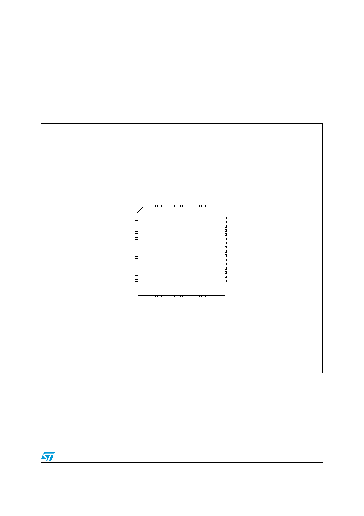
2 Package pinouts and signal descriptions
2.1 Package pinouts
The LQFP pinouts are shown in the following figures. For pin signal descriptions, please
refer to
Figure 2. 64-pin LQFP pinout – Full featured configuration (top view)
Ta bl e 7
VDD_HV_IO1
VSS_HV_IO1
VDD_HV_OSC
VSS_HV_OSC
VSS_LV_COR0
VDD_LV_COR0
.
RESET
NMI
A[6]
A[7]
A[8]
A[5]
D[9]
XTAL
EXTAL
D[8]
A[15]
A[14]
B[6]
A[13]
A[9]
VSS_LV_COR2
VDD_LV_COR2
C[8]
VSS_HV_IO3
VDD_HV_IO3
646362616059585756555453525150
1
2
3
4
5
6
7
8
9
10
11
12
13
14
15
16
LQFP64
A[12]
A[11]
A[10]
B[2]
B[1]
B[0]
49
A[4]
48
VPP TEST
47
D[14]]
46
D[12]
45
D[13
44
VSS_LV_COR1
43
VDD_LV_COR1
42
A[3]
41
VDD_HV_IO2
40
VSS_HV_IO2
39
TDO
38
TCK
37
TMS
36
TDI
35
C[12]
34
C[11]
33
171819202122232425
E[1]
B[7]
D[7]
C[1]
C[2]
B[8]
E[2]
B[9]
26272829303132
B[10]
B[11]
B[12]
E[3]/B[13]
VSS_HV_AD0
VDD_HV_AD0
BCTRL
VDD_HV_REG
Doc ID 16100 Rev 5 29/103

Package pinouts and signal descriptions SPC560P34L1, SPC560P34L3, SPC560P40L1,
Figure 3. 64-pin LQFP pinout – airbag configuration (top view)
A[15]
A[14]
B[6]
A[13]
A[9]
VSS_LV_COR2
VDD_LV_COR2
C[8]
VSS_HV_IO3
VDD_HV_IO3
A[12]
A[11]
A[10]
B[2]
B[1]]
B[0]
NMI
A[6]
A[7]
A[8]
A[5]
VDD_HV_IO1
VSS_HV_IO1
VDD_HV_OSC
VSS_HV_OSC
VSS_LV_COR0
VDD_LV_COR0
D[9]
XTAL
EXTAL
RESET
D[8]
646362616059585756555453525150
1
2
3
4
5
6
7
8
9
10
11
12
13
14
15
16
LQFP64
49
48
47
46
45
44
43
42
41
40
39
38
37
36
35
34
33
A[4]
VPP TEST
D[14]
D[12]
D[13]
VSS_LV_COR1
VDD_LV_COR1
A[3]
VDD_HV_IO2
VSS_HV_IO2
TDO
TCK
TMS
TDI
C[12]
C[11]
171819202122232425
E[1]
B[7]
D[7]
C[1]
C[2]
B[8]
E[2]
B[9]
26272829303132
B[10]
B[11]
B[12]
VSS_HV_AD0
VDD_HV_AD0
BCTRL
E[3]/B[13]
VDD_HV_REG
30/103 Doc ID 16100 Rev 5
 Loading...