

ST SPC560D30L3, SPC560D40L3, SPC560D30L1, SPC560D40L1 User Manual

Features
SPC560D30x
SPC560D40x
32-bit MCU family built on the Power Architecture
for automotive body electronics applications
Preliminary data
®
■ High-performance up to 48 MHz e200z0h CPU
– 32-bit Power Architecture
®
technology CPU
– Variable length encoding (VLE)
■ Memory
– Up to 256 KB Code Flash with ECC
– Up to 64 (4x16) KB Data Flash with ECC
– Up to 16 KB SRAM with ECC
■ Interrupts
– 16 priority levels
– Non-maskable interrupt (NMI)
– Up to 38 external interrupts incl. 18 wakeup
lines
■ 16-channel eDMA
■ GPIOs: 45 (LQFP64), 79 (LQFP100)
■ Timer units
– 4-channel 32-bit periodic interrupt timers
– 4-channel 32-bit system timer module
– System watchdog timer
– 32 bit real-time clock timer
■ 16-bit counter time-triggered I/Os
– Up to 28 channels with PWM/MC/IC/OC
– 5 independent counters
– 27 ch. with ADC trigger capability
■ 12-bit analog-to-digital converter (ADC) with up
to 33 channels
– Up to 61 channels via external multiplexing
– Individual conversion registers
– Cross triggering unit (CTU)
■ Dedicated diagnostic module for lighting
– Advanced PWM generation
– Time-triggered diagnostics
– PWM-synchronized ADC measurements
LQFP100 (14 x 14 x 1.4 mm)
■ Communications interfaces
LQFP64 (10 x 10 x 1.4 mm)
– 1 FlexCAN interface (2.0B active) with
32 message buffers
– 3 LINFlex/UART, 1 with DMA capability
–2 DSPI
■ Clock generation
– 4 to 16 MHz fast external crystal oscillator
– 16 MHz fast internal RC oscillator
– 128 kHz slow internal RC oscillator
– Software-controlled FMPLL
– Clock monitoring unit
■ Exhaustive debugging capability
– Nexus1 on all packages
– Nexus2+ available on emulation device
(SPC560B64B2-ENG)
■ On-chip CAN/UART bootstrap loader
■ Low power capabilities
– Several low power mode configurations
– Ultra-low power standby with RTC,SRAM
and CAN monitoring
– Fast wakeup schemes
■ Single 5 V or 3.3 V supply
■ Operates in ambient temperature range of
-40 to 125 °C
Table 1. Device summary
Part number
Package
LQFP100 SPC560D30L3 SPC560D40L3
LQFP64 SPC560D30L1 SPC560D40L1
128 Kbyte code
Flash
256 Kbyte code
Flash
December 2011 Doc ID 16315 Rev 5 1/82
This is preliminary information on a new product now in development or undergoing evaluation. Details are subject to
change without notice.
www.st.com
1

Contents SPC560D30x, SPC560D40x
Contents
1 Introduction . . . . . . . . . . . . . . . . . . . . . . . . . . . . . . . . . . . . . . . . . . . . . . . . 6
1.1 Document overview . . . . . . . . . . . . . . . . . . . . . . . . . . . . . . . . . . . . . . . . . . 6
1.2 Description . . . . . . . . . . . . . . . . . . . . . . . . . . . . . . . . . . . . . . . . . . . . . . . . . 6
2 Block diagram . . . . . . . . . . . . . . . . . . . . . . . . . . . . . . . . . . . . . . . . . . . . . . 8
3 Package pinouts and signal descriptions . . . . . . . . . . . . . . . . . . . . . . . 11
3.1 Package pinouts . . . . . . . . . . . . . . . . . . . . . . . . . . . . . . . . . . . . . . . . . . . . 11
3.2 Pad configuration during reset phases . . . . . . . . . . . . . . . . . . . . . . . . . . . 12
3.3 Voltage supply pins . . . . . . . . . . . . . . . . . . . . . . . . . . . . . . . . . . . . . . . . . 12
3.4 Pad types . . . . . . . . . . . . . . . . . . . . . . . . . . . . . . . . . . . . . . . . . . . . . . . . . 13
3.5 System pins . . . . . . . . . . . . . . . . . . . . . . . . . . . . . . . . . . . . . . . . . . . . . . . 13
3.6 Functional ports . . . . . . . . . . . . . . . . . . . . . . . . . . . . . . . . . . . . . . . . . . . . 14
4 Electrical characteristics . . . . . . . . . . . . . . . . . . . . . . . . . . . . . . . . . . . . 26
4.1 Introduction . . . . . . . . . . . . . . . . . . . . . . . . . . . . . . . . . . . . . . . . . . . . . . . 26
4.2 Parameter classification . . . . . . . . . . . . . . . . . . . . . . . . . . . . . . . . . . . . . . 26
4.3 NVUSRO register . . . . . . . . . . . . . . . . . . . . . . . . . . . . . . . . . . . . . . . . . . . 27
4.3.1 NVUSRO[PAD3V5V] field description . . . . . . . . . . . . . . . . . . . . . . . . . . 27
4.3.2 NVUSRO[OSCILLATOR_MARGIN] field description . . . . . . . . . . . . . . . 27
4.3.3 NVUSRO[WATCHDOG_EN] field description . . . . . . . . . . . . . . . . . . . . 27
4.4 Absolute maximum ratings . . . . . . . . . . . . . . . . . . . . . . . . . . . . . . . . . . . . 28
4.5 Recommended operating conditions . . . . . . . . . . . . . . . . . . . . . . . . . . . . 29
4.6 Thermal characteristics . . . . . . . . . . . . . . . . . . . . . . . . . . . . . . . . . . . . . . 31
4.6.1 Package thermal characteristics . . . . . . . . . . . . . . . . . . . . . . . . . . . . . . 31
4.6.2 Power considerations . . . . . . . . . . . . . . . . . . . . . . . . . . . . . . . . . . . . . . . 32
4.7 I/O pad electrical characteristics . . . . . . . . . . . . . . . . . . . . . . . . . . . . . . . 32
4.7.1 I/O pad types . . . . . . . . . . . . . . . . . . . . . . . . . . . . . . . . . . . . . . . . . . . . . 32
4.7.2 I/O input DC characteristics . . . . . . . . . . . . . . . . . . . . . . . . . . . . . . . . . . 32
4.7.3 I/O output DC characteristics . . . . . . . . . . . . . . . . . . . . . . . . . . . . . . . . . 34
4.7.4 Output pin transition times . . . . . . . . . . . . . . . . . . . . . . . . . . . . . . . . . . . 36
4.7.5 I/O pad current specification . . . . . . . . . . . . . . . . . . . . . . . . . . . . . . . . . 36
4.8 RESET electrical characteristics . . . . . . . . . . . . . . . . . . . . . . . . . . . . . . . 40
2/82 Doc ID 16315 Rev 5

SPC560D30x, SPC560D40x Contents
4.9 Power management electrical characteristics . . . . . . . . . . . . . . . . . . . . . 42
4.9.1 Voltage regulator electrical characteristics . . . . . . . . . . . . . . . . . . . . . . 42
4.9.2 Low voltage detector electrical characteristics . . . . . . . . . . . . . . . . . . . . 45
4.10 Power consumption . . . . . . . . . . . . . . . . . . . . . . . . . . . . . . . . . . . . . . . . . 46
4.11 Flash memory electrical characteristics . . . . . . . . . . . . . . . . . . . . . . . . . . 47
4.11.1 Program/Erase characteristics . . . . . . . . . . . . . . . . . . . . . . . . . . . . . . . . 47
4.11.2 Flash power supply DC characteristics . . . . . . . . . . . . . . . . . . . . . . . . . 49
4.11.3 Start-up/Switch-off timings . . . . . . . . . . . . . . . . . . . . . . . . . . . . . . . . . . . 50
4.12 Electromagnetic compatibility (EMC) characteristics . . . . . . . . . . . . . . . . 50
4.12.1 Designing hardened software to avoid noise problems . . . . . . . . . . . . . 50
4.12.2 Electromagnetic interference (EMI) . . . . . . . . . . . . . . . . . . . . . . . . . . . . 51
4.12.3 Absolute maximum ratings (electrical sensitivity) . . . . . . . . . . . . . . . . . 51
4.13 Fast external crystal oscillator (4 to 16 MHz) electrical characteristics . . 52
4.14 FMPLL electrical characteristics . . . . . . . . . . . . . . . . . . . . . . . . . . . . . . . 55
4.15 Fast internal RC oscillator (16 MHz) electrical characteristics . . . . . . . . . 56
4.16 Slow internal RC oscillator (128 kHz) electrical characteristics . . . . . . . . 57
4.17 ADC electrical characteristics . . . . . . . . . . . . . . . . . . . . . . . . . . . . . . . . . 58
4.17.1 Introduction . . . . . . . . . . . . . . . . . . . . . . . . . . . . . . . . . . . . . . . . . . . . . . 58
4.17.2 Input impedance and ADC accuracy . . . . . . . . . . . . . . . . . . . . . . . . . . . 58
4.17.3 ADC electrical characteristics . . . . . . . . . . . . . . . . . . . . . . . . . . . . . . . . 63
4.18 On-chip peripherals . . . . . . . . . . . . . . . . . . . . . . . . . . . . . . . . . . . . . . . . . 65
4.18.1 Current consumption . . . . . . . . . . . . . . . . . . . . . . . . . . . . . . . . . . . . . . . 65
4.18.2 DSPI characteristics . . . . . . . . . . . . . . . . . . . . . . . . . . . . . . . . . . . . . . . 67
4.18.3 JTAG characteristics . . . . . . . . . . . . . . . . . . . . . . . . . . . . . . . . . . . . . . . 72
5 Package characteristics . . . . . . . . . . . . . . . . . . . . . . . . . . . . . . . . . . . . . 73
5.1 ECOPACK
5.2 Package mechanical data . . . . . . . . . . . . . . . . . . . . . . . . . . . . . . . . . . . . 73
5.2.1 LQFP100 . . . . . . . . . . . . . . . . . . . . . . . . . . . . . . . . . . . . . . . . . . . . . . . . 73
5.2.2 LQFP64 . . . . . . . . . . . . . . . . . . . . . . . . . . . . . . . . . . . . . . . . . . . . . . . . . 75
® . . . . . . . . . . . . . . . . . . . . . . . . . . . . . . . . . . . . . . . . . . . . . . . . . . . . . . . . . . . . 73
6 Ordering information . . . . . . . . . . . . . . . . . . . . . . . . . . . . . . . . . . . . . . . 76
Appendix A Abbreviations. . . . . . . . . . . . . . . . . . . . . . . . . . . . . . . . . . . . . . . . . . . 77
Revision history . . . . . . . . . . . . . . . . . . . . . . . . . . . . . . . . . . . . . . . . . . . . . . . . . . . . 79
Doc ID 16315 Rev 5 3/82

List of tables SPC560D30x, SPC560D40x
List of tables
Table 2. SPC560D30, SPC560D40 device comparison . . . . . . . . . . . . . . . . . . . . . . . . . . . . . . . . . . . 6
Table 3. SPC560D30, SPC560D40 series block summary . . . . . . . . . . . . . . . . . . . . . . . . . . . . . . . . 9
Table 4. Voltage supply pin descriptions . . . . . . . . . . . . . . . . . . . . . . . . . . . . . . . . . . . . . . . . . . . . . 13
Table 5. System pin descriptions . . . . . . . . . . . . . . . . . . . . . . . . . . . . . . . . . . . . . . . . . . . . . . . . . . . 14
Table 6. Functional port pin descriptions . . . . . . . . . . . . . . . . . . . . . . . . . . . . . . . . . . . . . . . . . . . . . 14
Table 7. Parameter classifications . . . . . . . . . . . . . . . . . . . . . . . . . . . . . . . . . . . . . . . . . . . . . . . . . . 26
Table 8. PAD3V5V field description . . . . . . . . . . . . . . . . . . . . . . . . . . . . . . . . . . . . . . . . . . . . . . . . . 27
Table 9. OSCILLATOR_MARGIN field description. . . . . . . . . . . . . . . . . . . . . . . . . . . . . . . . . . . . . . 27
Table 10. WATCHDOG_EN field description . . . . . . . . . . . . . . . . . . . . . . . . . . . . . . . . . . . . . . . . . . . 27
Table 11. Absolute maximum ratings . . . . . . . . . . . . . . . . . . . . . . . . . . . . . . . . . . . . . . . . . . . . . . . . . 28
Table 12. Recommended operating conditions (3.3 V) . . . . . . . . . . . . . . . . . . . . . . . . . . . . . . . . . . . 29
Table 13. Recommended operating conditions (5.0 V) . . . . . . . . . . . . . . . . . . . . . . . . . . . . . . . . . . . 30
Table 14. LQFP thermal characteristics . . . . . . . . . . . . . . . . . . . . . . . . . . . . . . . . . . . . . . . . . . . . . . . 31
Table 15. I/O input DC electrical characteristics . . . . . . . . . . . . . . . . . . . . . . . . . . . . . . . . . . . . . . . . . 33
Table 16. I/O pull-up/pull-down DC electrical characteristics . . . . . . . . . . . . . . . . . . . . . . . . . . . . . . . 34
Table 17. SLOW configuration output buffer electrical characteristics . . . . . . . . . . . . . . . . . . . . . . . . 34
Table 18. MEDIUM configuration output buffer electrical characteristics . . . . . . . . . . . . . . . . . . . . . . 35
Table 19. Output pin transition times . . . . . . . . . . . . . . . . . . . . . . . . . . . . . . . . . . . . . . . . . . . . . . . . . 36
Table 20. I/O supply segment . . . . . . . . . . . . . . . . . . . . . . . . . . . . . . . . . . . . . . . . . . . . . . . . . . . . . . . 36
Table 21. I/O consumption . . . . . . . . . . . . . . . . . . . . . . . . . . . . . . . . . . . . . . . . . . . . . . . . . . . . . . . . . 37
Table 22. I/O weight . . . . . . . . . . . . . . . . . . . . . . . . . . . . . . . . . . . . . . . . . . . . . . . . . . . . . . . . . . . . . . 38
Table 23. Reset electrical characteristics . . . . . . . . . . . . . . . . . . . . . . . . . . . . . . . . . . . . . . . . . . . . . . 41
Table 24. Voltage regulator electrical characteristics . . . . . . . . . . . . . . . . . . . . . . . . . . . . . . . . . . . . . 44
Table 25. Low voltage detector electrical characteristics . . . . . . . . . . . . . . . . . . . . . . . . . . . . . . . . . . 46
Table 26. Power consumption on VDD_BV and VDD_HV . . . . . . . . . . . . . . . . . . . . . . . . . . . . . . . . . 46
Table 27. Program and erase specifications (code flash). . . . . . . . . . . . . . . . . . . . . . . . . . . . . . . . . . 48
Table 28. Program and erase specifications (data flash) . . . . . . . . . . . . . . . . . . . . . . . . . . . . . . . . . . 48
Table 29. Flash module life. . . . . . . . . . . . . . . . . . . . . . . . . . . . . . . . . . . . . . . . . . . . . . . . . . . . . . . . . 48
Table 30. Flash memory read access timing . . . . . . . . . . . . . . . . . . . . . . . . . . . . . . . . . . . . . . . . . . . 49
Table 31. Flash power supply DC electrical characteristics . . . . . . . . . . . . . . . . . . . . . . . . . . . . . . . . 49
Table 32. Start-up time/Switch-off time. . . . . . . . . . . . . . . . . . . . . . . . . . . . . . . . . . . . . . . . . . . . . . . . 50
Table 33. EMI radiated emission measurement . . . . . . . . . . . . . . . . . . . . . . . . . . . . . . . . . . . . . . . . . 51
Table 34. ESD absolute maximum ratings . . . . . . . . . . . . . . . . . . . . . . . . . . . . . . . . . . . . . . . . . . . . 52
Table 35. Latch-up results . . . . . . . . . . . . . . . . . . . . . . . . . . . . . . . . . . . . . . . . . . . . . . . . . . . . . . . . . 52
Table 36. Crystal description . . . . . . . . . . . . . . . . . . . . . . . . . . . . . . . . . . . . . . . . . . . . . . . . . . . . . . . 53
Table 37. Fast external crystal oscillator (4 to 16 MHz) electrical characteristics. . . . . . . . . . . . . . . . 54
Table 38. FMPLL electrical characteristics . . . . . . . . . . . . . . . . . . . . . . . . . . . . . . . . . . . . . . . . . . . . . 55
Table 39. Fast internal RC oscillator (16 MHz) electrical characteristics . . . . . . . . . . . . . . . . . . . . . . 56
Table 40. Slow internal RC oscillator (128 kHz) electrical characteristics . . . . . . . . . . . . . . . . . . . . . 57
Table 41. ADC input leakage current . . . . . . . . . . . . . . . . . . . . . . . . . . . . . . . . . . . . . . . . . . . . . . . . . 63
Table 42. ADC conversion characteristics . . . . . . . . . . . . . . . . . . . . . . . . . . . . . . . . . . . . . . . . . . . . . 63
Table 43. On-chip peripherals current consumption . . . . . . . . . . . . . . . . . . . . . . . . . . . . . . . . . . . . . . 65
Table 44. DSPI characteristics . . . . . . . . . . . . . . . . . . . . . . . . . . . . . . . . . . . . . . . . . . . . . . . . . . . . . . 67
Table 45. JTAG characteristics. . . . . . . . . . . . . . . . . . . . . . . . . . . . . . . . . . . . . . . . . . . . . . . . . . . . . . 72
Table 46. LQFP100 mechanical data . . . . . . . . . . . . . . . . . . . . . . . . . . . . . . . . . . . . . . . . . . . . . . . . . 74
Table 47. LQFP64 mechanical data . . . . . . . . . . . . . . . . . . . . . . . . . . . . . . . . . . . . . . . . . . . . . . . . . . 75
Table 48. Abbreviations . . . . . . . . . . . . . . . . . . . . . . . . . . . . . . . . . . . . . . . . . . . . . . . . . . . . . . . . . . . 77
Table 49. Document revision history . . . . . . . . . . . . . . . . . . . . . . . . . . . . . . . . . . . . . . . . . . . . . . . . . 79
4/82 Doc ID 16315 Rev 5

SPC560D30x, SPC560D40x List of figures
List of figures
Figure 1. SPC560D30, SPC560D40 series block diagram . . . . . . . . . . . . . . . . . . . . . . . . . . . . . . . . . 8
Figure 2. LQFP100 pin configuration (top view) . . . . . . . . . . . . . . . . . . . . . . . . . . . . . . . . . . . . . . . . 11
Figure 3. LQFP64 pin configuration (top view) . . . . . . . . . . . . . . . . . . . . . . . . . . . . . . . . . . . . . . . . . 12
Figure 4. Input DC electrical characteristics definition . . . . . . . . . . . . . . . . . . . . . . . . . . . . . . . . . . . . 33
Figure 5. Start-up reset requirements . . . . . . . . . . . . . . . . . . . . . . . . . . . . . . . . . . . . . . . . . . . . . . . . 40
Figure 6. Noise filtering on reset signal . . . . . . . . . . . . . . . . . . . . . . . . . . . . . . . . . . . . . . . . . . . . . . . 41
Figure 7. Voltage regulator capacitance connection . . . . . . . . . . . . . . . . . . . . . . . . . . . . . . . . . . . . . 43
Figure 8. Low voltage detector vs reset . . . . . . . . . . . . . . . . . . . . . . . . . . . . . . . . . . . . . . . . . . . . . . . 45
Figure 9. Crystal oscillator and resonator connection scheme . . . . . . . . . . . . . . . . . . . . . . . . . . . . . 53
Figure 10. Fast external crystal oscillator (4 to 16 MHz) timing diagram . . . . . . . . . . . . . . . . . . . . . . . 54
Figure 11. ADC characteristics and error definitions . . . . . . . . . . . . . . . . . . . . . . . . . . . . . . . . . . . . . . 58
Figure 12. Input equivalent circuit (precise channels) . . . . . . . . . . . . . . . . . . . . . . . . . . . . . . . . . . . . . 60
Figure 13. Input equivalent circuit (extended channels) . . . . . . . . . . . . . . . . . . . . . . . . . . . . . . . . . . . 60
Figure 14. Transient behavior during sampling phase . . . . . . . . . . . . . . . . . . . . . . . . . . . . . . . . . . . . . 61
Figure 15. Spectral representation of input signal . . . . . . . . . . . . . . . . . . . . . . . . . . . . . . . . . . . . . . . . 62
Figure 16. DSPI classic SPI timing – master, CPHA = 0 . . . . . . . . . . . . . . . . . . . . . . . . . . . . . . . . . . . 68
Figure 17. DSPI classic SPI timing – master, CPHA = 1 . . . . . . . . . . . . . . . . . . . . . . . . . . . . . . . . . . . 68
Figure 18. DSPI classic SPI timing – slave, CPHA = 0 . . . . . . . . . . . . . . . . . . . . . . . . . . . . . . . . . . . . 69
Figure 19. DSPI classic SPI timing – slave, CPHA = 1 . . . . . . . . . . . . . . . . . . . . . . . . . . . . . . . . . . . . 69
Figure 20. DSPI modified transfer format timing – master, CPHA = 0 . . . . . . . . . . . . . . . . . . . . . . . . . 70
Figure 21. DSPI modified transfer format timing – master, CPHA = 1 . . . . . . . . . . . . . . . . . . . . . . . . . 70
Figure 22. DSPI modified transfer format timing – slave, CPHA = 0 . . . . . . . . . . . . . . . . . . . . . . . . . . 71
Figure 23. DSPI modified transfer format timing – slave, CPHA = 1 . . . . . . . . . . . . . . . . . . . . . . . . . . 71
Figure 24. Timing diagram – JTAG boundary scan . . . . . . . . . . . . . . . . . . . . . . . . . . . . . . . . . . . . . . . 72
Figure 25. LQFP100 mechanical drawing . . . . . . . . . . . . . . . . . . . . . . . . . . . . . . . . . . . . . . . . . . . . . . 73
Figure 26. LQFP64 mechanical drawing . . . . . . . . . . . . . . . . . . . . . . . . . . . . . . . . . . . . . . . . . . . . . . . 75
Figure 27. Ordering information scheme . . . . . . . . . . . . . . . . . . . . . . . . . . . . . . . . . . . . . . . . . . . . . . . 76
Doc ID 16315 Rev 5 5/82
Introduction SPC560D30x, SPC560D40x
1 Introduction
1.1 Document overview
This document describes the device features and highlights the important electrical and
physical characteristics.
1.2 Description
These 32-bit automotive microcontrollers are a family of system-on-chip (SoC) devices
designed to be central to the development of the next wave of central vehicle body
controller, smart junction box, front module, peripheral body, door control and seat control
applications.
This family is one of a series of next-generation integrated automotive microcontrollers
based on the Power Architecture technology and designed specifically for embedded
applications.
The advanced and cost-efficient e200z0h host processor core of this automotive controller
family complies with the Power Architecture technology and only implements the VLE
(variable-length encoding) APU (auxiliary processing unit), providing improved code density.
It operates at speeds of up to 48 MHz and offers high performance processing optimized for
low power consumption. It capitalizes on the available development infrastructure of current
Power Architecture devices and is supported with software drivers, operating systems and
configuration code to assist with the user’s implementations.
The device platform has a single level of memory hierarchy and can support a wide range of
on-chip static random access memory (SRAM) and internal flash memory.
Feature
(2)
(3)
(4)
Device
SPC560D30L1 SPC560D30L3 SPC560D40L1 SPC560D40L3
(1)
14 ch, 16-bit 28 ch, 16-bit 14 ch, 16-bit 28 ch, 16-bit
2ch 5ch 2ch 5ch
—9ch—9ch
7ch 7ch 7ch 7ch
Table 2. SPC560D30, SPC560D40 device comparison
CPU e200z0h
Execution speed Static – up to 48 MHz
Code flash memory 128 KB 256 KB
Data flash memory 64 KB (4 × 16 KB)
SRAM 12 KB 16 KB
eDMA 16 ch
ADC (12-bit) 16 ch 33 ch 16 ch 33 ch
CTU 16 ch
Total timer I/O
eMIOS
– Type X
– Type Y
– Type G
6/82 Doc ID 16315 Rev 5

SPC560D30x, SPC560D40x Introduction
Table 2. SPC560D30, SPC560D40 device comparison (continued)
Device
Feature
SPC560D30L1 SPC560D30L3 SPC560D40L1 SPC560D40L3
(6)
(5)
4ch 7ch 4ch 7ch
45 79 45 79
– Type H
SCI (LINFlex) 3
SPI (DSPI) 2
CAN (FlexCAN) 1
GPIO
Debug JTAG
Package LQFP64 LQFP100 LQFP64 LQFP100
1. Refer to eMIOS chapter of device reference manual for information on the channel configuration and functions.
2. Type X = MC + MCB + OPWMT + OPWMB + OPWFMB + SAIC + SAOC.
3. Type Y = OPWMT + OPWMB + SAIC + SAOC.
4. Type G = MCB + IPWM + IPM + DAOC + OPWMT + OPWMB + OPWFMB + OPWMCB + SAIC + SAOC.
5. Type H = IPWM + IPM + DAOC + OPWMT + OPWMB + SAIC + SAOC.
6. I/O count based on multiplexing with peripherals.
Doc ID 16315 Rev 5 7/82

Block diagram SPC560D30x, SPC560D40x
2 Block diagram
Figure 1 shows a top-level block diagram of the SPC560D30, SPC560D40 device series.
Figure 1. SPC560D30, SPC560D40 series block diagram
JTAG Port
NMI
Clocks
Interrupt
Request
Request
Nexus 1
Voltage
Regulator
FMPLL
RTC
SIUL
Reset Control
External
Interrupt
Request
IMUX
GPIO &
Pad Control
JTAG
NMI
SIUL
Interrupt requests
from peripheral
CMU
STM
33 ch.
blocks
SWT
ADC
ECSM
e200z0h
PIT
CTU
INTC
Peripheral Bridge
1 x
eMIOS
Instructions
(Master)
Data
(Master)
eDMA
(Master)
LINFlex
3 x
SRAM
16 KB
SRAM
Controller
64-bit 3 x 3 Crossbar Switch
2 x
DSPI
(Slave)
MC_PCUMC_MEMC_CGMMC_RGM
Code Flash
256 KB
Controller
(Slave)
BAM
1 x
FlexCAN
Data Flash
64 KB
Flash
(Slave)
SSCM
WKPU
Interrupt
Request
I/O
Legend:
ADC Analog-to-Digital Converter
BAM Boot Assist Module
CMU Clock Monitor Unit
CTU Cross Triggering Unit
DSPI Deserial Serial Peripheral Interface
ECSM Error Correction Status Module
eDMA Enhanced Direct Memory Access
eMIOS Enhanced Modular Input Output System
Flash Flash memory
FlexCAN Controller Area Network (FlexCAN)
FMPLL Frequency-Modulated Phase-Locked Loop
IMUX Internal Multiplexer
INTC Interrupt Controller
JTAG JTAG controller
LINFlex Serial Communication Interface (LIN support)
. . .
. . .
MC_CGM Clock Generation Module
MC_ME Mode Entry Module
MC_PCU Power Control Unit
MC_RGM Reset Generation Module
NMI Non-Maskable Interrupt
PIT Periodic Interrupt Timer
RTC Real-Time Clock
SIUL System Integration Unit Lite
SRAM Static Random-Access Memory
SSCM System Status Configuration Module
STM System Timer Module
SWT Software Watchdog Timer
WKPU Wakeup Unit
XBAR Crossbar switch
8/82 Doc ID 16315 Rev 5
. . .
. . .

SPC560D30x, SPC560D40x Block diagram
Ta bl e 3 summarizes the functions of all blocks present in the SPC560D30, SPC560D40
series of microcontrollers. Please note that the presence and number of blocks varies by
device and package.
Table 3. SPC560D30, SPC560D40 series block summary
Analog-to-digital converter (ADC) Multi-channel, 12-bit analog-to digital-converter
Block Function
Boot assist module (BAM)
Clock generation module
(MC_CGM)
A block of read-only memory containing VLE code which is executed according
to the boot mode of the device
Provides logic and control required for the generation of system and peripheral
clocks
Clock monitor unit (CMU) Monitors clock source (internal and external) integrity
Cross triggering unit (CTU)
Enables synchronization of ADC conversions with a timer event from the eMIOS
or from the PIT
Supports simultaneous connections between two master ports and three slave
Crossbar switch (XBAR)
ports. The crossbar supports a 32-bit address bus width and a 64-bit data bus
width.
Deserial serial peripheral
interface (DSPI)
Enhanced direct memory access
(eDMA)
Enhanced modular input output
system (eMIOS)
Provides a synchronous serial interface for communication with external
devices
Performs complex data transfers with minimal intervention from a host
processor via “n” programmable channels.
Provides the functionality to generate or measure events
Provides a myriad of miscellaneous control functions for the device including
Error correction status module
(ECSM)
program-visible information about configuration and revision levels, a reset
status register, wakeup control for exiting sleep modes, and optional features
such as information on memory errors reported by error-correcting codes
Flash memory Provides non-volatile storage for program code, constants and variables
FlexCAN (controller area
network)
Supports the standard CAN communications protocol
Frequency-modulated phaselocked loop (FMPLL)
Internal multiplexer (IMUX) SIU
subblock
Generates high-speed system clocks and supports programmable frequency
modulation
Allows flexible mapping of peripheral interface on the different pins of the device
Interrupt controller (INTC) Provides priority-based preemptive scheduling of interrupt requests
JTAG controller (JTAGC)
LINFlex controller
Provides the means to test chip functionality and connectivity while remaining
transparent to system logic when not in test mode
Manages a high number of LIN (Local Interconnect Network protocol)
messages efficiently with a minimum of CPU load
Provides a mechanism for controlling the device operational mode and mode
Mode entry module (MC_ME)
transition sequences in all functional states; also manages the power control
unit, reset generation module and clock generation module, and holds the
configuration, control and status registers accessible for applications
Non-maskable interrupt (NMI)
Handles external events that must produce an immediate response, such as
power down detection
Doc ID 16315 Rev 5 9/82

Block diagram SPC560D30x, SPC560D40x
Table 3. SPC560D30, SPC560D40 series block summary (continued)
Block Function
Periodic interrupt timer (PIT) Produces periodic interrupts and triggers
Reduces the overall power consumption by disconnecting parts of the device
Power control unit (MC_PCU)
from the power supply via a power switching device; device components are
grouped into sections called “power domains” which are controlled by the PCU
Real-time counter (RTC)
Reset generation module
(MC_RGM)
Static random-access memory
(SRAM)
Provides a free-running counter and interrupt generation capability that can be
used for timekeeping applications
Centralizes reset sources and manages the device reset sequence of the
device
Provides storage for program code, constants, and variables
Provides control over all the electrical pad controls and up 32 ports with 16 bits
System integration unit lite (SIUL)
of bidirectional, general-purpose input and output signals and supports up to 32
external interrupts with trigger event configuration
System status and configuration
module (SSCM)
System timer module (STM)
Provides system configuration and status data (such as memory size and
status, device mode and security status), device identification data, debug
status port enable and selection, and bus and peripheral abort enable/disable
Provides a set of output compare events to support AUTOSAR (Automotive
Open System Architecture) and operating system tasks
Software watchdog timer (SWT) Provides protection from runaway code
Supports up to 18 external sources that can generate interrupts or wakeup
Wakeup unit (WKPU)
events, of which 1 can cause non-maskable interrupt requests or wakeup
events.
10/82 Doc ID 16315 Rev 5

SPC560D30x, SPC560D40x Package pinouts and signal descriptions
3 Package pinouts and signal descriptions
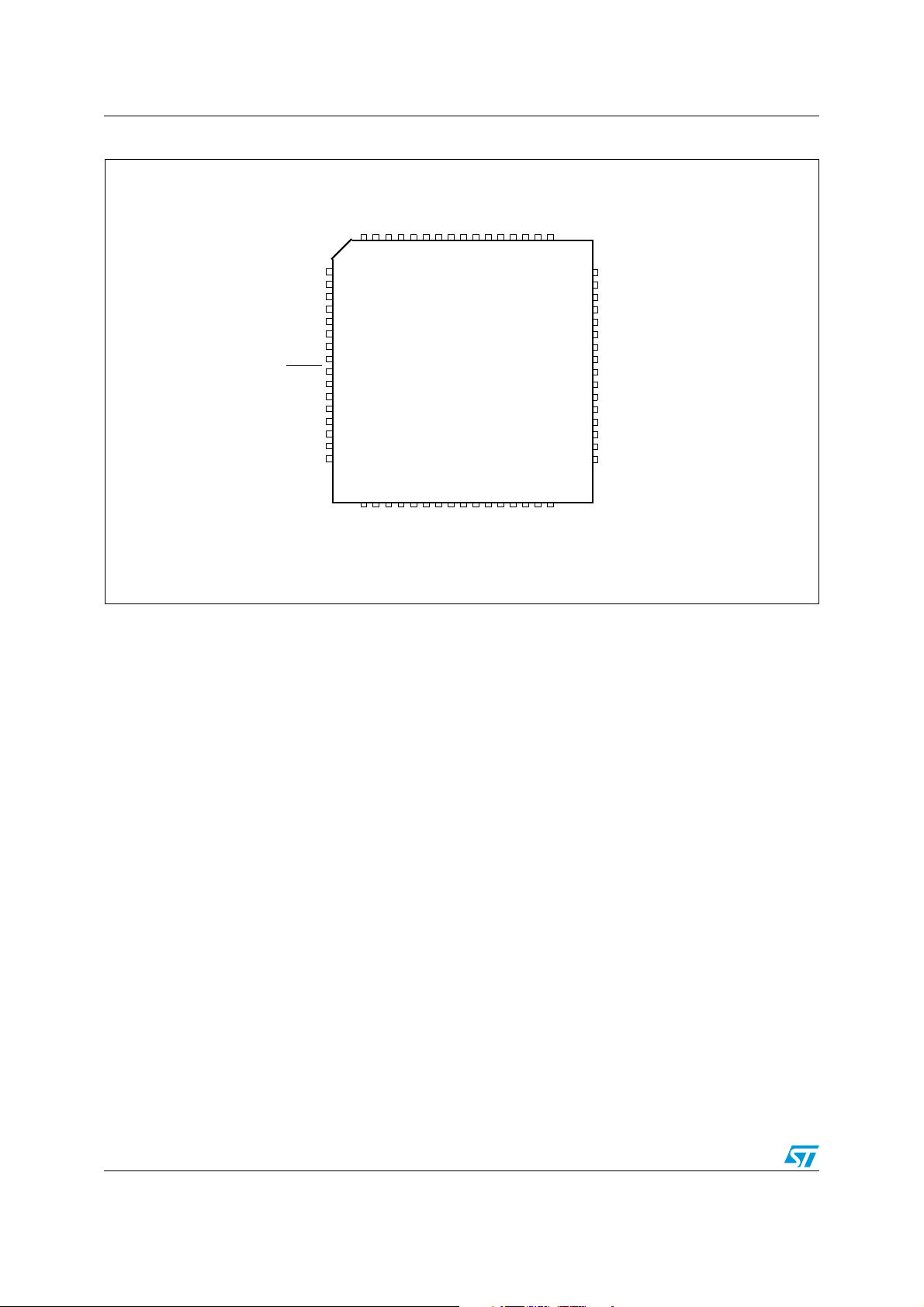
3.1 Package pinouts
The available LQFP pinouts are provided in the following figures. For pin signal descriptions,
please refer to Tab l e 6 .
Figure 2 shows the SPC560D30, SPC560D40 in the LQFP100 package.
Figure 2. LQFP100 pin configuration (top view)
PB[2]
PC[8]
PC[13]
PC[12]
PE[7]
PE[6]
PE[5]
PE[4]
PC[4]
PC[5]
PE[3]
PE[2]
PH[9]
PC[0]
VSS_LV
VDD_LV
VDD_HV
VSS_HV
PC[1]
PH[10]
PA [ 6]
PA [ 5]
PC[2]
PC[3]
PE[12]
PB[3]
PC[9]
PC[14]
PC[15]
PA [2 ]
PE[0]
PA [1 ]
PE[1]
PE[8]
PE[9]
PE[10]
PA [0 ]
PE[11]
VSS_HV
VDD_HV
VSS_HV
RESET
VSS_LV
VDD_LV
VDD_BV
PC[11]
PC[10]
PB[0]
PB[1]
PC[6]
9998979695949392919089888786858483828180797877
100
1
2
3
4
5
6
7
8
9
10
11
12
13
14
15
16
17
18
19
20
21
22
23
24
25
26272829303132333435363738394041424344454647484950
PA [4 ]
PC[7]
PA[15]
PA[14]
PA[13]
PA[12]
VDD_LV
LQFP100
XTAL
VSS_LV
VSS_HV
EXTAL
VDD_HV
PB[9]
PB[8]
PD[0]
PD[1]
PD[2]
PD[3]
PB[10]
PD[4]
76
75
PA[11]
74
PA[10]
73
PA [ 9]
72
PA [ 8]
71
PA [ 7]
70
VDD_HV
69
VSS_HV
68
PA [ 3]
67
PB[15]
66
PD[15]
65
PB[14]
64
PD[14]
63
PB[13]
62
PD[13]
61
PB[12]
60
PD[12]
59
PB[11]
58
PD[11]
57
PD[10]
56
PD[9]
55
PB[7]
54
PB[6]
53
PB[5]
52
VDD_HV_ADC
51
VSS_HV_ADC
PD[5]
PB[4]
PD[6]
PD[7]
PD[8]
Figure 3 shows the SPC560D30, SPC560D40 in the LQFP64 package.
Doc ID 16315 Rev 5 11/82
Package pinouts and signal descriptions SPC560D30x, SPC560D40x
Figure 3. LQFP64 pin configuration (top view)
PB[2]
PC[8]
PC[4]
PC[5]
PH[9]
PC[0]
VSS_LV
VDD_LV
VDD_HV
VSS_HV
PC[1]
PH[10]
PA [6 ]
PA [5 ]
PC[2]
PC[3]
PB[3]
PC[9]
PA [2 ]
PA [1 ]
PA [0 ]
VSS_HV
VDD_HV
VSS_HV
RESET
VSS_LV
VDD_LV
VDD_BV
PC[10]
PB[0]
PB[1]
PC[6]
646362616059585756555453525150
1
2
3
4
5
6
7
8
9
10
11
12
13
14
15
16
171819202122232425
PC[7]
PA[15]
PA[14]
PA [4 ]
LQFP64
PA[13]
PA[12]
VSS_LV
VDD_LV
26272829303132
XTAL
VSS_HV
EXTAL
VDD_HV
49
48
47
46
45
44
43
42
41
40
39
38
37
36
35
34
33
PB[9]
PB[8]
PB[4]
PB[10]
3.2 Pad configuration during reset phases
All pads have a fixed configuration under reset.
PA [1 1 ]
PA [1 0 ]
PA [9 ]
PA [8 ]
PA [7 ]
PA [3 ]
PB[15]
PB[14]
PB[13]
PB[12]
PB[11]
PB[7]
PB[6]
PB[5]
VDD_HV_ADC
VSS_HV_ADC
During the power-up phase, all pads are forced to tristate.
After power-up phase, all pads are forced to tristate with the following exceptions:
● PA[9] (FAB) is pull-down. Without external strong pull-up the device starts fetching from
flash.
● PA[8] (ABS[0]) is pull-up.
● RESET pad is driven low. This is pull-up only after PHASE2 reset completion.
● JTAG pads (TCK, TMS and TDI) are pull-up whilst TDO remains tristate.
● Precise ADC pads (PB[7:4] and PD[11:0]) are left tristate (no output buffer available).
● Main oscillator pads (EXTAL, XTAL) are tristate.
3.3 Voltage supply pins
Voltage supply pins are used to provide power to the device. Two dedicated pins are used
for 1.2 V regulator stabilization.
12/82 Doc ID 16315 Rev 5

SPC560D30x, SPC560D40x Package pinouts and signal descriptions
Table 4. Voltage supply pin descriptions
Pin number
Port pin Function
LQFP64 LQFP100
VDD_HV Digital supply voltage 7, 28, 34, 56 15, 37, 52, 70, 84
VSS_HV Digital ground 6, 8, 26, 33, 55 14, 16, 35, 51, 69, 83
VDD_LV
VSS_LV
1.2V decoupling pins. Decoupling capacitor must be
connected between these pins and the nearest V
(1)
pin.
SS_LV
1.2V decoupling pins. Decoupling capacitor must be
connected between these pins and the nearest V
(1)
pin.
DD_LV
11, 23, 57 19, 32, 85
10, 24, 58 18, 33, 86
VDD_BV Internal regulator supply voltage 12 20
1. A decoupling capacitor must be placed between each of the three VDD_LV/VSS_LV supply pairs to ensure stable voltage
(see the recommended operating conditions in the device datasheet for details).
3.4 Pad types
In the device the following types of pads are available for system pins and functional port
pins:
S = Slow
M = Medium
F = Fast
I = Input only with analog feature
J = Input/Output (‘S’ pad) with analog feature
X = Oscillator
(a)
(a) (b)
(a) (b)
(a)
3.5 System pins
The system pins are listed in Ta bl e 5 .
a. See the I/O pad electrical characteristics in the device datasheet for details.
b. All medium and fast pads are in slow configuration by default at reset and can be configured as fast or medium
(see the PCR[SRC] description in the device reference manual).
Doc ID 16315 Rev 5 13/82

Package pinouts and signal descriptions SPC560D30x, SPC560D40x
Table 5. System pin descriptions
Port
pin
RESET
Function
Bidirectional reset with Schmitt-Trigger
characteristics and noise filter.
Analog output of the oscillator amplifier
circuit, when the oscillator is not in bypass
EXTAL
mode.
Analog input for the clock generator when the
oscillator is in bypass mode.
(1)
Analog input of the oscillator amplifier circuit.
XTAL
1. Refer to the relevant section of the device datasheet.
Needs to be grounded if oscillator is used in
bypass mode.
(1)
3.6 Functional ports
The functional port pins are listed in Ta bl e 6 .
Table 6. Functional port pin descriptions
I/O
direction
Pad
type
RESET
configuration
Pin number
LQFP64 LQFP100
Input, weak
I/O M
pull-up only
917
after PHASE2
I/O X Tristate 27 36
I X Tristate 25 34
Port pin PCR
PA[0] PCR[0]
PA[1] PCR[1]
PA[2] PCR[2]
Alternate
function
AF0
AF1
AF2
AF3
—
AF0
AF1
AF2
AF3
—
—
AF0
AF1
AF2
AF3
—
Function Peripheral
(1)
GPIO[0]
E0UC[0]
CLKOUT
E0UC[13]
WKPU[19]
(3)
GPIO[1]
E0UC[1]
—
—
(4)
NMI
WKPU[2]
(3)
GPIO[2]
E0UC[2]
—
MA[2]
WKPU[3]
(3)
Por t A
SIUL
eMIOS_0
CGL
eMIOS_0
WKPU
SIUL
eMIOS_0
—
—
WKPU
WKPU
SIUL
eMIOS_0
—
ADC
WKPU
I/O
direction
(2)
I/O
I/O
O
I/O
I
I/O
I/O
—
—
I
I
I/O
I/O
—
O
I
Pin number
Pad
type
RESET
LQFP64 LQFP100
configuration
M Tristate 5 12
S Tristate 4 7
S Tristate 3 5
14/82 Doc ID 16315 Rev 5

SPC560D30x, SPC560D40x Package pinouts and signal descriptions
Table 6. Functional port pin descriptions (continued)
Port pin PCR
PA[3] PCR[3]
PA[4] PCR[4]
PA[5] PCR[5]
PA[6] PCR[6]
Alternate
function
AF0
AF1
AF2
AF3
—
—
AF0
AF1
AF2
AF3
—
AF0
AF1
AF2
AF3
AF0
AF1
AF2
AF3
—
Function Peripheral
(1)
GPIO[3]
E0UC[3]
—
CS4_0
EIRQ[0]
ADC1_S[0]
GPIO[4]
E0UC[4]
—
CS0_1
WKPU[9]
(3)
GPIO[5]
E0UC[5]
—
—
GPIO[6]
E0UC[6]
—
CS1_1
EIRQ[1]
SIUL
eMIOS_0
—
DSPI_0
SIUL
ADC
SIUL
eMIOS_0
—
DSPI_1
WKPU
SIUL
eMIOS_0
—
—
SIUL
eMIOS_0
—
DSPI_1
SIUL
I/O
direction
(2)
I/O
I/O
—
I/O
I
I
I/O
I/O
—
I/O
I
I/O
I/O
—
—
I/O
I/O
—
I/O
I
Pin number
Pad
type
RESET
LQFP64 LQFP100
configuration
S Tristate 43 68
S Tristate 20 29
M Tristate 51 79
S Tristate 52 80
PA[7] PCR[7]
PA[8] PCR[8]
PA[9] PCR[9]
AF0
AF1
AF2
AF3
AF0
AF1
AF2
AF3
N/A
AF0
AF1
AF2
AF3
N/A
—
—
—
(5)
(5)
GPIO[7]
E0UC[7]
—
—
EIRQ[2]
ADC1_S[1]
GPIO[8]
E0UC[8]
E0UC[14]
—
EIRQ[3]
ABS[0]
GPIO[9]
E0UC[9]
—
CS2_1
FAB
SIUL
eMIOS_0
—
—
SIUL
ADC
SIUL
eMIOS_0
eMIOS_0
—
SIUL
BAM
SIUL
eMIOS_0
—
DSPI_1
BAM
I/O
I/O
—
—
I/O
I/O
—
—
I/O
I/O
—
I/O
S Tristate 44 71
I
I
Input,
S
weak pull-
45 72
up
I
I
S Pull-down 46 73
I
Doc ID 16315 Rev 5 15/82

Package pinouts and signal descriptions SPC560D30x, SPC560D40x
Table 6. Functional port pin descriptions (continued)
Port pin PCR
PA[10] PCR[10]
PA[11] PCR[11]
PA[12] PCR[12]
Alternate
function
AF0
AF1
AF2
AF3
—
AF0
AF1
AF2
AF3
—
—
—
AF0
AF1
AF2
AF3
—
—
Function Peripheral
(1)
GPIO[10]
E0UC[10]
—
LIN2TX
ADC1_S[2]
GPIO[11]
E0UC[11]
—
—
EIRQ[16]
ADC1_S[3]
LIN2RX
GPIO[12]
—
—
—
EIRQ[17]
SIN_0
SIUL
eMIOS_0
—
LINFlex_2
ADC
SIUL
eMIOS_0
—
—
SIUL
ADC
LINFlex_2
SIUL
—
—
—
SIUL
DSPI_0
I/O
direction
(2)
I/O
I/O
—
O
I
I/O
I/O
—
—
I
I
I
I/O
—
—
—
I
I
Pin number
Pad
type
RESET
LQFP64 LQFP100
configuration
S Tristate 47 74
S Tristate 48 75
S Tristate 22 31
PA[13] PCR[13]
PA[14] PCR[14]
PA[15] PCR[15]
PB[0] PCR[16]
AF0
AF1
AF2
AF3
AF0
AF1
AF2
AF3
—
AF0
AF1
AF2
AF3
—
AF0
AF1
AF2
AF3
GPIO[13]
SOUT_0
—
CS3_1
GPIO[14]
SCK_0
CS0_0
E0UC[0]
EIRQ[4]
GPIO[15]
CS0_0
SCK_0
E0UC[1]
WKPU[10]
GPIO[16]
CAN0TX
—
LIN2TX
(3)
FlexCAN_0
SIUL
DSPI_0
—
DSPI_1
SIUL
DSPI_0
DSPI_0
eMIOS_0
SIUL
SIUL
DSPI_0
DSPI_0
eMIOS_0
WKPU
Por t B
SIUL
—
LINFlex_2
I/O
O
—
I/O
I/O
I/O
I/O
I/O
I/O
I/O
I/O
I/O
I/O
O
—
O
M Tristate 21 30
M Tristate 19 28
I
M Tristate 18 27
I
M Tristate 14 23
16/82 Doc ID 16315 Rev 5

SPC560D30x, SPC560D40x Package pinouts and signal descriptions
Table 6. Functional port pin descriptions (continued)
Port pin PCR
PB[1] PCR[17]
PB[2] PCR[18]
PB[3] PCR[19]
PB[4] PCR[20]
PB[5] PCR[21]
PB[6] PCR[22]
PB[7] PCR[23]
Alternate
function
AF0
AF1
AF2
AF3
—
—
AF0
AF1
AF2
AF3
AF0
AF1
AF2
AF3
—
—
AF0
AF1
AF2
AF3
—
AF0
AF1
AF2
AF3
—
AF0
AF1
AF2
AF3
—
AF0
AF1
AF2
AF3
—
Function Peripheral
(1)
GPIO[17]
—
—
LIN0RX
WKPU[4]
(3)
CAN0RX
GPIO[18]
LIN0TX
—
—
GPIO[19]
—
—
—
WKPU[11]
(3)
LIN0RX
GPIO[20]
—
—
—
ADC1_P[0]
GPIO[21]
—
—
—
ADC1_P[1]
GPIO[22]
—
—
—
ADC1_P[2]
GPIO[23]
—
—
—
ADC1_P[3]
SIUL
—
—
LINFlex_0
WKPU
FlexCAN_0
SIUL
LINFlex_0
—
—
SIUL
—
—
—
WKPU
LINFlex_0
SIUL
—
—
—
ADC
SIUL
—
—
—
ADC
SIUL
—
—
—
ADC
SIUL
—
—
—
ADC
I/O
direction
(2)
I/O
—
—
I
I
I
I/O
O
—
—
I/O
—
—
—
I
I
I
—
—
—
I
I
—
—
—
I
I
—
—
—
I
I
—
—
—
I
Pin number
Pad
type
RESET
LQFP64 LQFP100
configuration
S Tristate 15 24
M Tristate 64 100
S Tristate 1 1
I Tristate 32 50
I Tristate 35 53
I Tristate 36 54
I Tristate 37 55
Doc ID 16315 Rev 5 17/82

Package pinouts and signal descriptions SPC560D30x, SPC560D40x
Table 6. Functional port pin descriptions (continued)
Port pin PCR
PB[8] PCR[24]
PB[9] PCR[25]
PB[10] PCR[26]
Alternate
function
AF0
AF1
AF2
AF3
—
—
AF0
AF1
AF2
AF3
—
—
AF0
AF1
AF2
AF3
—
—
Function Peripheral
(1)
GPIO[24]
—
—
—
ADC1_S[4]
WKPU[25]
(3)
GPIO[25]
—
—
—
ADC1_S[5]
WKPU[26]
(3)
GPIO[26]
—
—
—
ADC1_S[6]
WKPU[8]
(3)
SIUL
—
—
—
ADC
WKPU
SIUL
—
—
—
ADC
WKPU
SIUL
—
—
—
ADC
WKPU
I/O
direction
(2)
I
—
—
—
I
I
I
—
—
—
I
I
I/O
—
—
—
I
I
Pin number
Pad
type
RESET
LQFP64 LQFP100
configuration
I Tristate 30 39
I Tristate 29 38
J Tristate 31 40
PB[11] PCR[27]
PB[12] PCR[28]
PB[13] PCR[29]
PB[14] PCR[30]
AF0
AF1
AF2
AF3
—
AF0
AF1
AF2
AF3
—
AF0
AF1
AF2
AF3
—
AF0
AF1
AF2
AF3
—
GPIO[27]
E0UC[3]
—
CS0_0
ADC1_S[12]
GPIO[28]
E0UC[4]
—
CS1_0
ADC1_X[0]
GPIO[29]
E0UC[5]
—
CS2_0
ADC1_X[1]
GPIO[30]
E0UC[6]
—
CS3_0
ADC1_X[2]
SIUL
eMIOS_0
—
DSPI_0
ADC
SIUL
eMIOS_0
—
DSPI_0
ADC
SIUL
eMIOS_0
—
DSPI_0
ADC
SIUL
eMIOS_0
—
DSPI_0
ADC
I/O
I/O
—
I/O
I/O
I/O
—
O
I/O
I/O
—
O
I/O
I/O
—
O
J Tristate 38 59
I
J Tristate 39 61
I
J Tristate 40 63
I
J Tristate 41 65
I
18/82 Doc ID 16315 Rev 5

SPC560D30x, SPC560D40x Package pinouts and signal descriptions
Table 6. Functional port pin descriptions (continued)
Port pin PCR
PB[15] PCR[31]
(6)
(6)
PCR[32]
PCR[33]
PC[0]
PC[1]
PC[2] PCR[34]
Alternate
function
AF0
AF1
AF2
AF3
—
AF0
AF1
AF2
AF3
AF0
AF1
AF2
AF3
AF0
AF1
AF2
AF3
—
Function Peripheral
(1)
GPIO[31]
E0UC[7]
—
CS4_0
ADC1_X[3]
GPIO[32]
—
TDI
—
GPIO[33]
—
TDO
—
GPIO[34]
SCK_1
—
—
EIRQ[5]
SIUL
eMIOS_0
—
DSPI_0
ADC
Por t C
SIUL
—
JTAGC
—
SIUL
—
JTAGC
—
SIUL
DSPI_1
—
—
SIUL
I/O
direction
(2)
I/O
I/O
—
O
I
I/O
—
I
—
I/O
—
O
—
I/O
I/O
—
—
I
Pin number
Pad
type
RESET
LQFP64 LQFP100
configuration
J Tristate 42 67
Input,
M
weak pull-
59 87
up
F Tristate 54 82
M Tristate 50 78
PC[3] PCR[35]
PC[4] PCR[36]
PC[5] PCR[37]
PC[6] PCR[38]
AF0
AF1
AF2
AF3
—
AF0
AF1
AF2
AF3
—
—
AF0
AF1
AF2
AF3
—
AF0
AF1
AF2
AF3
GPIO[35]
CS0_1
MA[0]
—
EIRQ[6]
GPIO[36]
—
—
—
SIN_1
EIRQ[18]
GPIO[37]
SOUT_1
—
—
EIRQ[7]
GPIO[38]
LIN1TX
—
—
SIUL
DSPI_1
ADC
—
SIUL
SIUL
—
—
—
DSPI_1
SIUL
SIUL
DSPI_1
—
—
SIUL
SIUL
LINFlex_1
—
—
I/O
I/O
O
—
I/O
—
—
—
I/O
O
—
—
I/O
O
—
—
S Tristate 49 77
I
M Tristate 62 92
I
I
M Tristate 61 91
I
S Tristate 16 25
Doc ID 16315 Rev 5 19/82

Package pinouts and signal descriptions SPC560D30x, SPC560D40x
Table 6. Functional port pin descriptions (continued)
Port pin PCR
PC[7] PCR[39]
PC[8] PCR[40]
PC[9] PCR[41]
PC[10] PCR[42]
Alternate
function
AF0
AF1
AF2
AF3
—
—
AF0
AF1
AF2
AF3
AF0
AF1
AF2
AF3
—
—
AF0
AF1
AF2
AF3
Function Peripheral
(1)
GPIO[39]
—
—
—
LIN1RX
WKPU[12]
(3)
GPIO[40]
LIN2TX
E0UC[3]
—
GPIO[41]
—
E0UC[7]
—
LIN2RX
WKPU[13]
(3)
GPIO[42]
—
—
MA[1]
SIUL
—
—
—
LINFlex_1
WKPU
SIUL
LINFlex_2
eMIOS_0
—
SIUL
—
eMIOS_0
—
LINFlex_2
WKPU
SIUL
—
—
ADC
I/O
direction
(2)
I/O
—
—
—
I
I
I/O
O
I/O
—
I/O
—
I/O
—
I
I
I/O
—
—
O
Pin number
Pad
type
RESET
LQFP64 LQFP100
configuration
S Tristate 17 26
S Tristate 63 99
S Tristate 2 2
M Tristate 13 22
PC[11] PCR[43]
PC[12] PCR[44]
PC[13] PCR[45]
PC[14] PCR[46]
AF0
AF1
AF2
AF3
—
AF0
AF1
AF2
AF3
—
AF0
AF1
AF2
AF3
AF0
AF1
AF2
AF3
—
GPIO[43]
—
—
MA[2]
WKPU[5]
GPIO[44]
E0UC[12]
—
—
EIRQ[19]
GPIO[45]
E0UC[13]
—
—
GPIO[46]
E0UC[14]
—
—
EIRQ[8]
(3)
SIUL
—
—
ADC
WKPU
SIUL
eMIOS_0
—
—
SIUL
SIUL
eMIOS_0
—
—
SIUL
eMIOS_0
—
—
SIUL
I/O
—
—
O
I/O
I/O
—
—
I/O
I/O
—
—
I/O
I/O
—
—
S Tristate — 21
I
M Tristate — 97
I
S Tristate — 98
S Tristate — 3
I
20/82 Doc ID 16315 Rev 5

SPC560D30x, SPC560D40x Package pinouts and signal descriptions
Table 6. Functional port pin descriptions (continued)
Port pin PCR
PC[15] PCR[47]
PD[0] PCR[48]
PD[1] PCR[49]
PD[2] PCR[50]
PD[3] PCR[51]
PD[4] PCR[52]
PD[5] PCR[53]
Alternate
function
AF0
AF1
AF2
AF3
—
AF0
AF1
AF2
AF3
—
—
AF0
AF1
AF2
AF3
—
—
AF0
AF1
AF2
AF3
—
AF0
AF1
AF2
AF3
—
AF0
AF1
AF2
AF3
—
AF0
AF1
AF2
AF3
—
Function Peripheral
(1)
GPIO[47]
E0UC[15]
—
—
EIRQ[20]
GPIO[48]
—
—
—
WKPU[27]
(3)
ADC1_P[4]
GPIO[49]
—
—
—
WKPU[28]
(3)
ADC1_P[5]
GPIO[50]
—
—
—
ADC1_P[6]
GPIO[51]
—
—
—
ADC1_P[7]
GPIO[52]
—
—
—
ADC1_P[8]
GPIO[53]
—
—
—
ADC1_P[9]
SIUL
eMIOS_0
—
—
SIUL
Por t D
SIUL
—
—
—
WKPU
ADC
SIUL
—
—
—
WKPU
ADC
SIUL
—
—
—
ADC
SIUL
—
—
—
ADC
SIUL
—
—
—
ADC
SIUL
—
—
—
ADC
I/O
direction
(2)
I/O
I/O
—
—
I
I
—
—
—
I
I
I
—
—
—
I
I
I
—
—
—
I
I
—
—
—
I
I
—
—
—
I
I
—
—
—
I
Pin number
Pad
type
RESET
LQFP64 LQFP100
configuration
M Tristate — 4
I Tristate — 41
I Tristate — 42
I Tristate — 43
I Tristate — 44
I Tristate — 45
I Tristate — 46
Doc ID 16315 Rev 5 21/82

Package pinouts and signal descriptions SPC560D30x, SPC560D40x
Table 6. Functional port pin descriptions (continued)
Port pin PCR
PD[6] PCR[54]
PD[7] PCR[55]
PD[8] PCR[56]
PD[9] PCR[57]
Alternate
function
AF0
AF1
AF2
AF3
—
AF0
AF1
AF2
AF3
—
AF0
AF1
AF2
AF3
—
AF0
AF1
AF2
AF3
—
Function Peripheral
(1)
GPIO[54]
—
—
—
ADC1_P[10]
GPIO[55]
—
—
—
ADC1_P[11]
GPIO[56]
—
—
—
ADC1_P[12]
GPIO[57]
—
—
—
ADC1_P[13]
SIUL
—
—
—
ADC
SIUL
—
—
—
ADC
SIUL
—
—
—
ADC
SIUL
—
—
—
ADC
I/O
direction
(2)
I
—
—
—
I
I
—
—
—
I
I
—
—
—
I
I
—
—
—
I
Pin number
Pad
type
RESET
LQFP64 LQFP100
configuration
I Tristate — 47
I Tristate — 48
I Tristate — 49
I Tristate — 56
PD[10] PCR[58]
PD[11] PCR[59]
PD[12] PCR[60]
PD[13] PCR[61]
AF0
AF1
AF2
AF3
—
AF0
AF1
AF2
AF3
—
AF0
AF1
AF2
AF3
—
AF0
AF1
AF2
AF3
—
GPIO[58]
—
—
—
ADC1_P[14]
GPIO[59]
—
—
—
ADC1_P[15]
GPIO[60]
CS5_0
E0UC[24]
—
ADC1_S[8]
GPIO[61]
CS0_1
E0UC[25]
—
ADC1_S[9]
SIUL
—
—
—
ADC
SIUL
—
—
—
ADC
SIUL
DSPI_0
eMIOS_0
—
ADC
SIUL
DSPI_1
eMIOS_0
—
ADC
—
—
—
—
—
—
I/O
O
I/O
—
I/O
I/O
I/O
—
I
I Tristate — 57
I
I
I Tristate — 58
I
J Tristate — 60
I
J Tristate — 62
I
22/82 Doc ID 16315 Rev 5

SPC560D30x, SPC560D40x Package pinouts and signal descriptions
Table 6. Functional port pin descriptions (continued)
Port pin PCR
PD[14] PCR[62]
PD[15] PCR[63]
PE[0] PCR[64]
PE[1] PCR[65]
PE[2] PCR[66]
PE[3] PCR[67]
PE[4] PCR[68]
PE[5] PCR[69]
Alternate
function
AF0
AF1
AF2
AF3
—
AF0
AF1
AF2
AF3
—
AF0
AF1
AF2
AF3
—
AF0
AF1
AF2
AF3
AF0
AF1
AF2
AF3
—
—
AF0
AF1
AF2
AF3
AF0
AF1
AF2
AF3
—
AF0
AF1
AF2
AF3
Function Peripheral
(1)
GPIO[62]
CS1_1
E0UC[26]
—
ADC1_S[10]
GPIO[63]
CS2_1
E0UC[27]
—
ADC1_S[11]
GPIO[64]
E0UC[16]
—
—
WKPU[6]
(3)
GPIO[65]
E0UC[17]
—
—
GPIO[66]
E0UC[18]
—
—
EIRQ[21]
SIN_1
GPIO[67]
E0UC[19]
SOUT_1
—
GPIO[68]
E0UC[20]
SCK_1
—
EIRQ[9]
GPIO[69]
E0UC[21]
CS0_1
MA[2]
SIUL
DSPI_1
eMIOS_0
—
ADC
SIUL
DSPI_1
eMIOS_0
—
ADC
Por t E
SIUL
eMIOS_0
—
—
WKPU
SIUL
eMIOS_0
—
—
SIUL
eMIOS_0
—
—
SIUL
DSPI_1
SIUL
eMIOS_0
DSPI_1
—
SIUL
eMIOS_0
DSPI_1
—
SIUL
SIUL
eMIOS_0
DSPI_1
ADC
I/O
direction
(2)
I/O
O
I/O
—
I
I/O
O
I/O
—
I
I/O
I/O
—
—
I
I/O
I/O
—
—
I/O
I/O
—
—
I
I
I/O
I/O
O
—
I/O
I/O
I/O
—
I
I/O
I/O
I/O
O
Pin number
Pad
type
RESET
LQFP64 LQFP100
configuration
J Tristate — 64
J Tristate — 66
S Tristate — 6
M Tristate — 8
M Tristate — 89
M Tristate — 90
M Tristate — 93
M Tristate — 94
Doc ID 16315 Rev 5 23/82

Package pinouts and signal descriptions SPC560D30x, SPC560D40x
Table 6. Functional port pin descriptions (continued)
Port pin PCR
PE[6] PCR[70]
PE[7] PCR[71]
PE[8] PCR[72]
PE[9] PCR[73]
PE[10] PCR[74]
PE[11] PCR[75]
PE[12] PCR[76]
Alternate
function
AF0
AF1
AF2
AF3
—
AF0
AF1
AF2
AF3
—
AF0
AF1
AF2
AF3
AF0
AF1
AF2
AF3
—
AF0
AF1
AF2
AF3
—
AF0
AF1
AF2
AF3
—
AF0
AF1
AF2
AF3
—
—
Function Peripheral
(1)
GPIO[70]
E0UC[22]
CS3_0
MA[1]
EIRQ[22]
GPIO[71]
E0UC[23]
CS2_0
MA[0]
EIRQ[23]
GPIO[72]
—
E0UC[22]
—
GPIO[73]
—
E0UC[23]
—
WKPU[7]
(3)
GPIO[74]
—
CS3_1
—
EIRQ[10]
GPIO[75]
E0UC[24]
CS4_1
—
WKPU[14]
(3)
GPIO[76]
—
—
—
ADC1_S[7]
EIRQ[11]
SIUL
eMIOS_0
DSPI_0
ADC
SIUL
SIUL
eMIOS_0
DSPI_0
ADC
SIUL
SIUL
—
eMIOS_0
—
SIUL
—
eMIOS_0
—
WKPU
SIUL
—
DSPI_1
—
SIUL
SIUL
eMIOS_0
DSPI_1
—
WKPU
SIUL
—
—
—
ADC
SIUL
I/O
direction
(2)
I/O
I/O
O
O
I
I/O
I/O
O
O
I
I/O
—
I/O
—
I/O
—
I/O
—
I
I/O
—
O
—
I
I/O
I/O
O
—
I
I/O
—
—
—
I
I
Pin number
Pad
type
RESET
LQFP64 LQFP100
configuration
M Tristate — 95
M Tristate — 96
M Tristate — 9
S Tristate — 10
S Tristate — 11
S Tristate — 13
S Tristate — 76
Por t H
24/82 Doc ID 16315 Rev 5

SPC560D30x, SPC560D40x Package pinouts and signal descriptions
Table 6. Functional port pin descriptions (continued)
Pin number
LQFP64 LQFP100
Port pin PCR
Alternate
function
Function Peripheral
(1)
I/O
direction
(2)
Pad
type
RESET
configuration
AF0
PH[9]
(6)
PCR[121]
AF1
AF2
AF3
AF0
PH[10]
(6)
PCR[122]
AF1
AF2
AF3
1. Alternate functions are chosen by setting the values of the PCR.PA bitfields inside the SIUL module. PCR.PA = 00 → AF0;
PCR.PA = 01 → AF1; PCR.PA = 10 → AF2; PCR.PA = 11 → AF3. This is intended to select the output functions; to use
one of the input functions, the PCR.IBE bit must be written to ‘1’, regardless of the values selected in the PCR.PA bitfields.
For this reason, the value corresponding to an input only function is reported as “—”.
2. Multiple inputs are routed to all respective modules internally. The input of some modules must be configured by setting the
values of the PSMIO.PADSELx bitfields inside the SIUL module.
3. All WKPU pins also support external interrupt capability. See “wakeup unit” chapter of the device reference manual for
further details.
4. NMI has higher priority than alternate function. When NMI is selected, the PCR.AF field is ignored.
5. “Not applicable” because these functions are available only while the device is booting. Refer to “BAM” chapter of the
device reference manual for details.
6. Out of reset all the functional pins except PC[0:1] and PH[9:10] are available to the user as GPIO.
PC[0:1] are available as JTAG pins (TDI and TDO respectively).
PH[9:10] are available as JTAG pins (TCK and TMS respectively).
If the user configures these JTAG pins in GPIO mode the device is no longer compliant with IEEE 1149.1 2001.
GPIO[121]
—
TCK
—
GPIO[122]
—
TMS
—
SIUL
—
JTAGC
—
SIUL
—
JTAGC
—
I/O
—
—
I/O
—
—
Input,
S
I
weak pull-
up
60 88
Input,
S
I
weak pull-
up
53 81
Doc ID 16315 Rev 5 25/82
 Loading...