

SMP75-8
FEATURES
Bidirectionalsurgearrestor.
Verylow stand-offvoltage : V
Highrepetitive surgecapability:
I
= 75A (10/1000µs).
PP
Verylow capacitance: C < 75pF
Low leakagecurrent :< 2 µA
DESCRIPTION
TheSMP75-8 isa very lowvoltagetransient surge
arrestor especially designed to protect sensitive
telecommunication equipment against lightning
strikesand othertransients.
MAINAPPLICATION
XDSLTRANSMISSIONEQUIPMENT
RM
=8V.
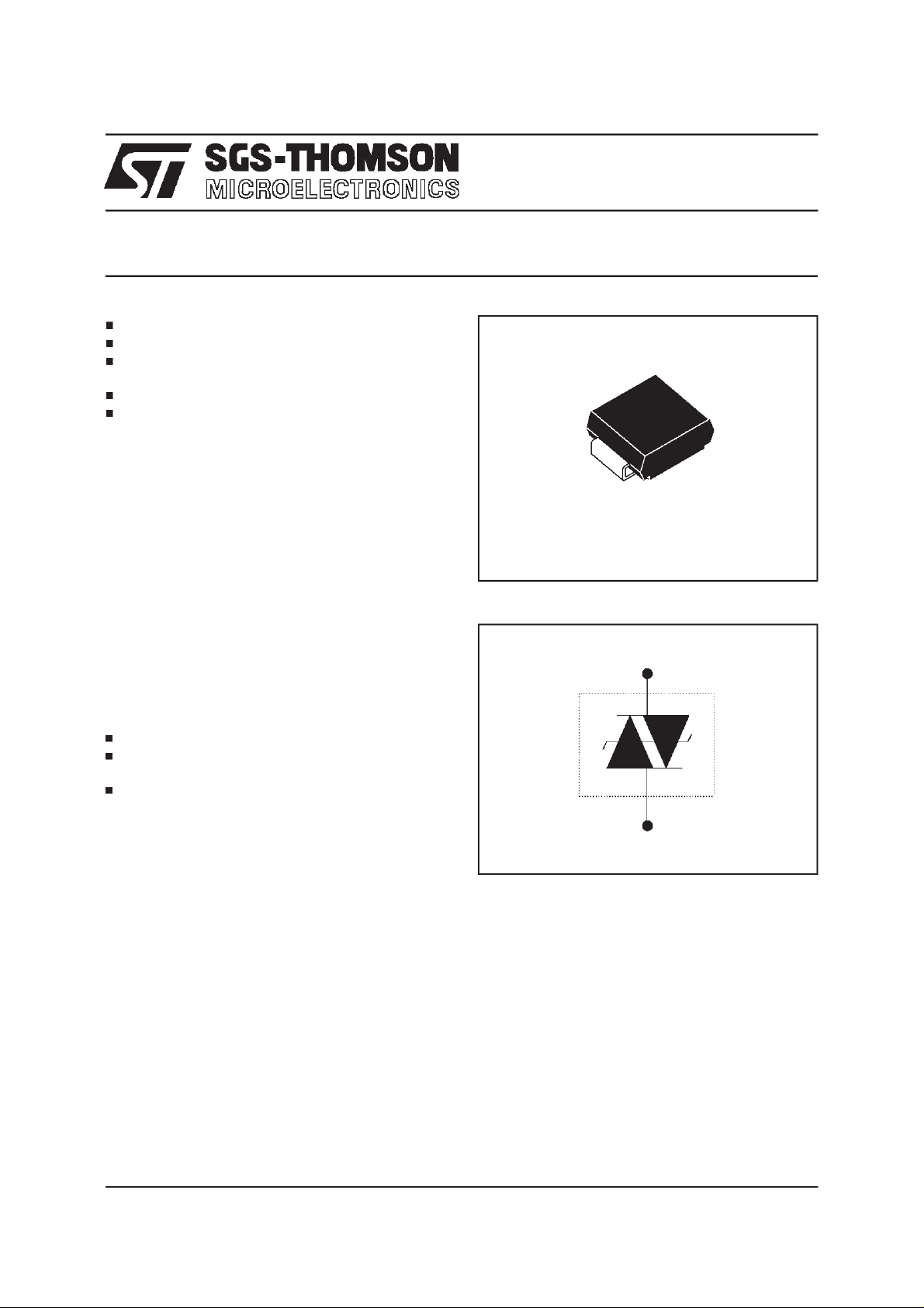
SMB
(JEDEC DO-214AA)
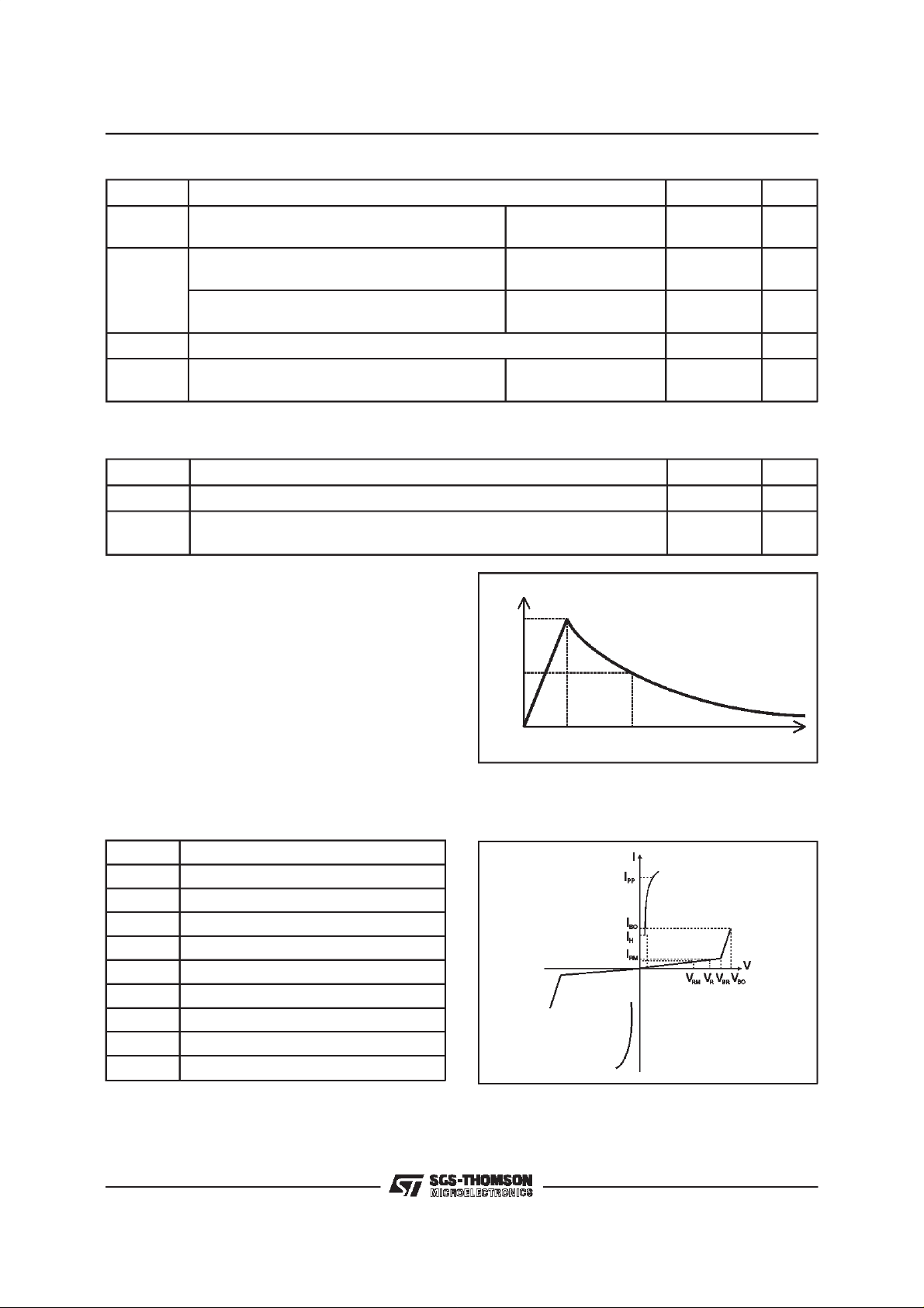
SCHEMATIC DIAGRAM
TRISIL
TM
BENEFITS
Protectionagainsthigh energysurges.
Very low breakover voltage : V
avoiding saturationof transformer.
No signal distortion thanks to very low capacitance.
COMPLIESWITHTHEFOLLOWINGSTANDAR DS:
- BELLCORETR-NWT
-000974: 10/1000µs1kV
10/1000µs 75A*
- CCITT K20: 10/700µs4kV
5/310µs 100A
- VDE 0433: 10/700µs4kV
5/310µs 100A
- VDE 0878: 1.2/50 µs4kV
1/20 µs 100A
* with series resistor or PTC.
< 15 V, thus
BO
January 1998- Ed : 2
1/6
SMP75-8
ABSOLUTE MAXIMUMRATINGS (T
amb
=
25°C)
Symbol Parameter Value Unit
I
I
TSM
T
T
Tj
pp
stg
Peak pulsecurrent 10/1000µs
8/20µs
Non repetitivesurge peakon-state current
One cycle
Non repetitivesurge peakon-state current
F = 50Hz
Maximumlead temperaturefor solderingduring 10s 260 °C
I
Storagetemperaturerange
50Hz
60Hz
0.2s
2s
- 55 to+ 150
Maximumjunction temperature
75
250
35
37
14
6
150
THERMAL RESISTANCES
Symbol Parameter Value Unit
R
R
th(j-I)
th(j-a)
Junctionto leads 20 °C/W
Junctionto ambient onprinted circuit
100 °C/W
(withstandardfootprint dimensions)
Note 1:
Pulsewaveform
%I
PP
A
A
A
A
A
A
°C
°C
10 /1000µstr=10µs tp = 1000
8/20µstr=8µstp=20µs
5 / 310µstr=5µs tp = 310µs
1/20µstr=1µstp=20µs
2/10µstr=2
µ
stp=10
ELECTRICALCHARACTERISTICS(T
Symbol Parameter
V
RM
I
RM
V
R
V
BR
V
BO
I
H
I
BO
I
PP
Stand-offvoltage
Leakagecurrent atstand-offvoltage
ContinuousReversevoltage
Breakdownvoltage
Breakovervoltage
Holdingcurrent
Breakovercurrent
Peak pulsecurrent
C Capacitance
amb
µ
s
µ
s
=25°C)
100
50
0
t
rp
t
2/6

STATICPARAMETERS
SMP75-8
Type
I
RM
max.
@V
RM
I
@V
R
max.
note1
V
R
BO
@I
BO
max.
note 2
I
H
typ.
note 3
µAVµAV V mA mA pF
SMP75-8 2 6 50 8 15 800 50 75
Note 1 : IRmeasuredat VRguaranteesVBR>V
Note 2 : Measured at 50Hz,see test circuit 1.In anycase V
Note 3 : See functional holdingcurrent test circuit2.
Note 4 :
VR=1V bias,V
=1V, F=1MHz.
RMS
R
BOmin
≥ V
BR
DYNAMICPARAMETERS
Symbol Test conditions (see note5) Type Max. Unit
Test conditions 1
V
= 100V/µs, di/dt< 10 A/µs, IPP=75A
V
BO
RISE
SMP75-8 20 V
Test conditions 2
V
= 1kV/µs, di/dt< 10 A/µs,IPP=10A
RISE
Note 5 : VBOparameters are givenby a KeyTek’System 2’ generatorwith PN246I module.
Seetest circuits (3) for VBOdynamic parameters.
C
max.
note 4
TESTCIRCUIT 1 FORI
Auto
Transformer
220V/2A
220V
TESTPROCEDURE :
PulseTest duration(tp = 20ms):
- ForBidirectionaldevices= SwitchK isclosed
- ForUnidirectionaldevices = SwitchK isopen.
V
Selection
OUT
- Devicewith V
-V
OUT
- Devicewith V
-V
OUT
andVBOparameters:
BO
V
out
Transformer
220V/800 V
5A
< 200Volt
BO
= 250V
≥ 200Volt
BO
= 480V
,R1=140 Ω.
RMS
RMS,R2
tp
static
relay.
measure
= 240Ω.
= 20ms
K
I
BO
R1
140
R2
240
D.U.T
V
BO
measure
3/6

SMP75-8
FUNCTIONAL HOLDINGCURRENT (IH) TESTCIRCUIT2: GO-NOGO TEST
R
-V
P
V
BAT
=-6
D.U.T .
V
Surge generator
Thisis aGO-NOGOtestwhichallowsto confirmthe holdingcurrent(IH)levelin afunctionaltestcircuit.
TESTPROCEDURE :
- Adjustthe currentlevel at theI
- Firethe D.U.T.with a surgecurrent : I
- TheD.U.T. willcome backto theOFF-statewithin adurationof 50ms max.
valueby short circuitingthe D.U.T.
H
= 10A,10/1000 µs.
pp
TESTCIRCUITS3 FORVBODYNAMICPARAMETERS
100 V / µs,
U
KeyTek ’System 2’ generator with PN246Imodule
1kV/µs,
U
Ipp = 75A
10 µF
Ipp = 10 A
26 µH
60 µF
2 Ω
45 Ω
250Ω
12 Ω
47 Ω
66 Ω
470 Ω
46 µH
83 Ω
0.36nF
46 µH
KeyTek ’System2’ generator with PN246I module
4/6

TYPICALAPPLICATION: T1 / E1protection
SMP75-8
DA108S1
+Vcc
RX LINE
SMP75-8
TX LINE
+Vcc
SMP75-8
The above schematicshows a T1 /E1 application
circuit. Thistype of line protection may be used in
premises equipment or telephone company
equipment on ports directly connected to metallic
plantlines.
During the lightning surge, the low voltage Trisil
SMP75-8
provides an efficient crowbar protection
ontheprimaryside of thetransformer.
The SMP75-8has a maximumpeak pulse current
of 75A (10/1000µs pulse) and a maximum
breakover voltage of 15V. This low voltage
prevents the transformer to be satured when a
surge occurs on the line. Additionally, the low
capacitance(65pF) is required to avoid significant
signaldegradation inthecase of highspeeddigital
pulses.
To protectthe IC lineinterface from the remaining
energy which is coupled through the transformer,
RTIP
+Vcc
RRING
IC
TTIP
+Vcc
TRING
SM6T6V8A
additional voltage protection is recommended on
the line input / output pins of the IC. The diode
array DA108S1 connected between +Vcc and
GND is then used to limit the remaining
overvoltagewithin a safelevel.
The DA108S1 is especially dedicated to this
application because. Its fast response time and
low forward voltage drop enable it to clamp any
surge before the IC line interface internal
protection fails. Additionally, the low capacitance
(30pF)is requiredto prevent signaldegradation of
thehigh speeddatd.
The DA108S1 is a fully integrated (1 chip) device
and results from the ST ASD
Specific Discretes) technology. ASDs
TM
(Application
TM
combine
the functions of several components into a single
monolithicdevice thatis tailoredto meet the exact
requirement of a specific application, allowing
higherdensity andimproved reliability.
5V
0V
ORDERCODE
SURFACEMOUNT
TRISIL75 A
SMP 75 - 8
VOLTAGE
5/6

SMP75-8
Non repetitivesurge peak current versusoverload
duration.
TSM (A)
I
50
45
40
35
30
25
20
15
10
5
0
1E-2 1E-1 1E+0 1E+1 1E+2 1E+3
t(s)
F=50Hz
Tj initial=25°C
PACKAGEMECHANICALDATA
SMB(JEDEC DO-214AA)(Plastic)
E1
D
E
A1
c
L
A2
b
MARKING
Package Type Marking
SMB SMP75-8 L08
DIMENSIONS
REF.
Millimeters Inches
Min. Typ. Max. Min. Typ. Max.
A1 1.90 2.15 2.45 0.075 0.085 0.096
A2 0.05 0.15 0.20 0.002 0.006 0.008
b 1.95 2.20 0.077 0.087
c 0.15 0.41 0.006 0.016
E 5.10 5.40 5.60 0.201 0.213 0.220
E1 4.05 4.30 4.60 0.159 0.169 0.181
D 3.30 3.60 3.95 0.130 0.142 0.156
L 0.75 1.15 1.60 0.030 0.045 0.063
FOOTPRINT
(in millimeters)
Packaging: tapeand reel
Weight: 0.12g
2.3
1.52 2.75
Information furnished is believed to be accurate and reliable. However, SGS-THOMSON Microelectronics assumes no responsibility for the
consequences of use of such information nor forany infringement of patents or other rights of third partieswhich may result from its use. No
license is grantedby implication or otherwise underany patent or patentrights ofSGS-THOMSON Microelectronics.Specifications mentioned
in this publicationare subjectto changewithout notice. This publicationsupersedes and replaces all informationpreviously supplied.
SGS-THOMSONMicroelectronics productsare notauthorizedfor use as criticalcomponentsin life support devices or systemswithout express
writtenapproval of SGS-THOMSON Microelectronics.
1998 SGS-THOMSON Microelectronics - Printed in Italy -All rights reserved.
Australia - Brazil - Canada - China - France - Germany -Italy - Japan - Korea- Malaysia - Malta - Morocco
The Netherlands- Singapore - Spain - Sweden -Switzerland - Taiwan - Thailand -United Kingdom -U.S.A.
6/6
1.52
SGS-THOMSON MicroelectronicsGROUP OF COMPANIES
 Loading...