

Datasheet SMP50-100, SMP50-120, SMP50-130, SMP50-180, SMP50-200 Datasheet (SGS Thomson Microelectronics)
...
®
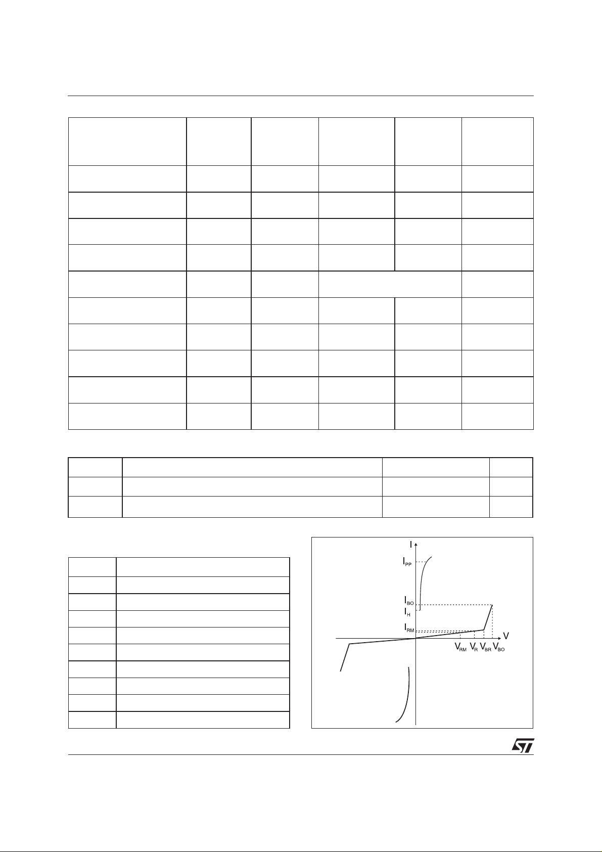
TELECOM EQUIPMENT PROTECTION: TRISIL™
FEATURES
Bidirectional crowbar protection
■
Voltage range from 62V to 270V
■
Low capacitance from 15pF to 30pF typ.@ 50V
■
Low leakage current: IR= 2µA max.
■
Holding current: IH= 150 mA min.
■
Repetitive peak pulse current:
■
= 50 A (10/1000 µs)
I
PP
MAIN APPLICATIONS
Telecommunication equipment such as
Analog and digital line cards (xDSL, T1/E1,
■
ISDN...).
Terminals (phone, fax, modem...) and central
■
office equipment.
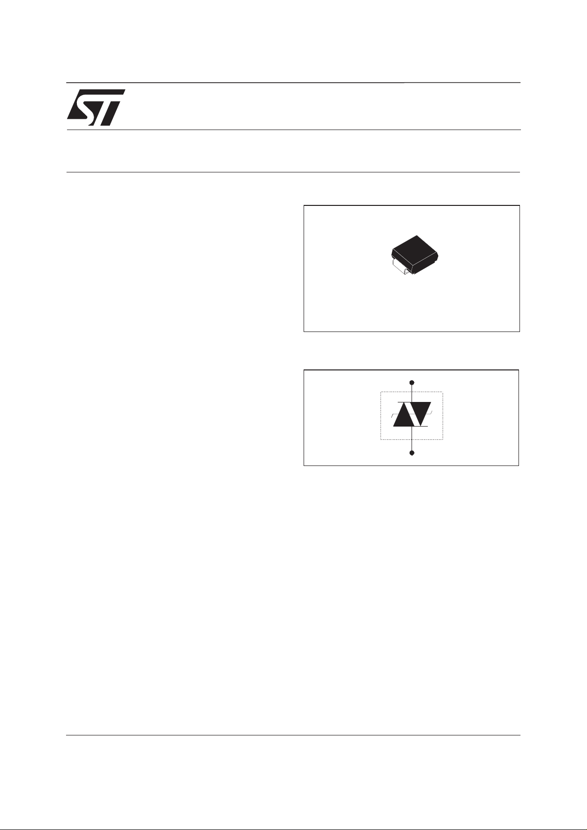
SMP50-xxx
SMA
(JEDEC DO-214AC)
SCHEMATIC DIAGRAM
DESCRIPTION
The SMP50-xxx series has been designed to
protect telecommunication equipment against
lightningandtransientinduced byACpower lines.
The package/ die sizeratio has been optimizedby
using the SMA package.
BENEFITS
Trisils are not subject to ageing and provide a fail safe mode in short circuit for a better protection. Trisils
are used to help equipment to meet various standards such as UL1950, IEC950 / CSA C22.2, UL1459
and FCC part 68. Trisils have UL94 V0resinapproved.SMA package is JEDEC registred. (Trisils are UL
497B approved - file: E136224).
November 2002- Ed: 3B
1/8
SMP50-xxx
IN COMPLIANCES WITH THE FOLLOWING STANDARDS
Standard
GR-1089 Core
First level
GR-1089 Core
Second level
GR-1089 Core
Intra-building
ITU-T-K20 / K21
ITU-T-K20
(IEC61000-4-2)
VDE0433
VDE0878
IEC61000-4-5
FCC Part 68, lightning
surge type A
FCC Part 68, lightning
surge type B
Peak Surge
Voltage
(V)
2500
1000
Voltage
Waveform
(µs)
2/10
10/1000
Required peak
current (A)
500
100
Current
Waveform
(µs)
2/10
10/1000
5000 2/10 500 2/10 24
1500 2/10 100 2/10 0
6000
1500
6000
8000
4000
2000
4000
2000
4000
4000
1500
800
10/700
1/60 ns
10/700
1.2/50
10/700
1.2/50
10/160
10/560
150
37.5
5/310
ESD contact discharge
ESD air discharge
100
50
100
50
100
100
200
100
5/310
1/20
5/310
8/20
10/160
10/560
1000 9/720 25 5/320 0
Minimum
serial resistor
to meet
standard (Ω)
12
10
53
0
0
0
21.5
0
0
0
21.5
0
12.5
6.5
THERMAL RESISTANCES
Symbol Parameter Value Unit
R
(j-a)
th
(j-l)
R
th
Junction to ambient with recommended footprint
Junction to leads
120 °C/W
30 °C/W
ELECTRICAL CHARACTERISTICS
= 25°C)
(T
amb
Symbol Parameter
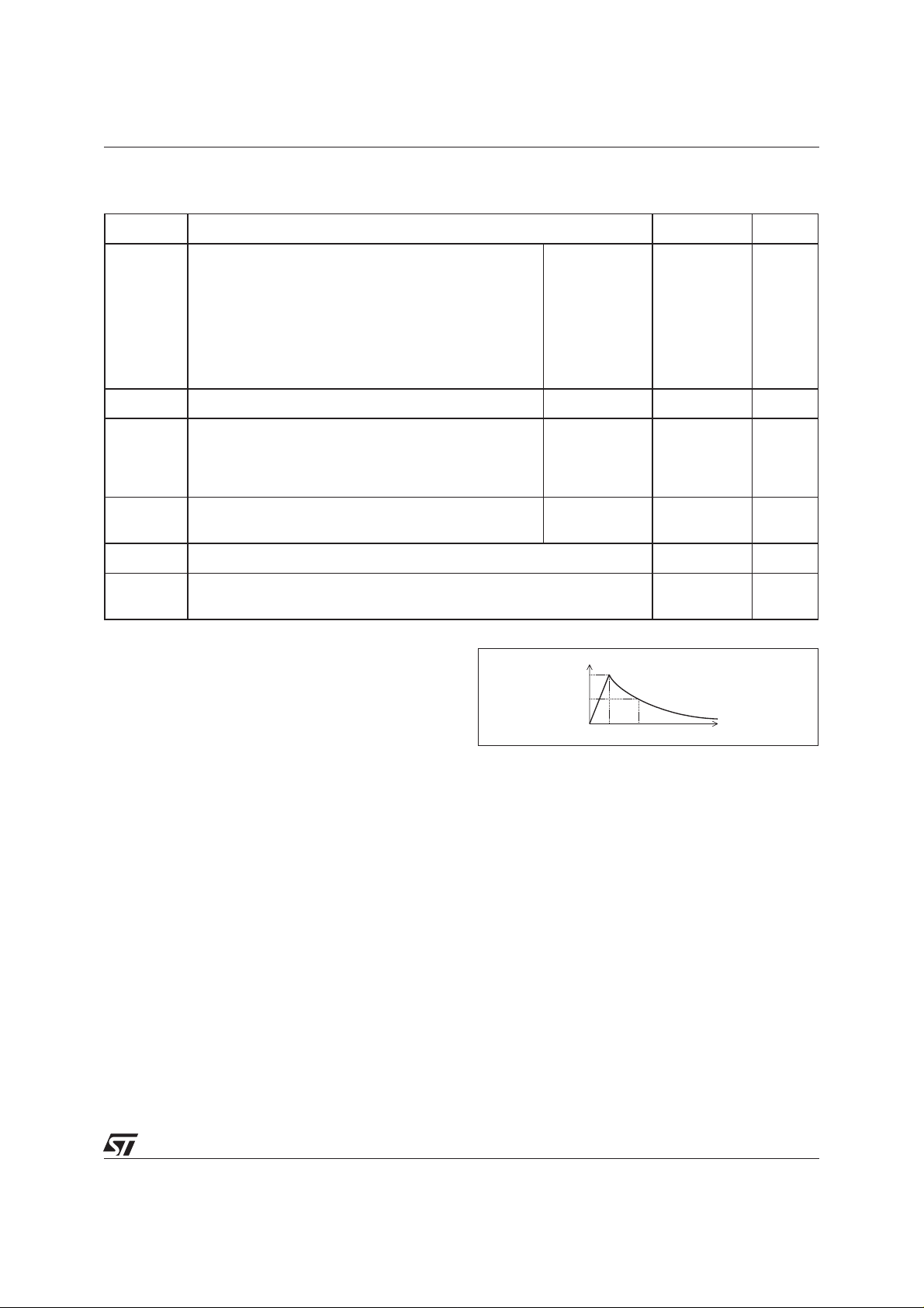
V
RM
I
RM
V
R
V
BR
V
BO
I
H
I
BO
I
PP
C
Stand-off voltage
Leakage current at V
RM
Continuous reverse voltage
Breakdown voltage
Breakover voltage
Holding current
Breakover current
Peak pulse current
Capacitance
2/8
SMP50-xxx
ABSOLUTE RATINGS (T
amb
= 25°C)
Symbol Parameter Value Unit
Repetitive peak pulse current:
I
I
I
TSM
I²t
T
T
T
PP
FS
stg
10/1000 µs
8/20 µs
10/560 µs
5/310 µs
10/160 µs
1/20 µs
2/10 µs
Fail safe mode: maximum current (note 1)
Non repetitive surge peak on-state current
(Sinusoidal)
8/20 µs 2.5 kA
t = 20ms
t = 16.6ms
t = 0.2s
t=2s
I²t value for fusing
t = 16.6ms
t = 20ms
L
Maximum lead temperature for soldering during 10 s.
Storage temperature range
j
Maximum junction temperature
50
100
55
65
75
100
150
25
28
16
8.5
6.5
6.3
260 °C
-55to+150
150
A
A
A²s
°C
°C
Repetitive peak pulse current
tr: rise time (µs)
tp: pulse duration time (µs)
ex: Pulse waveform 10/1000µs
tr = 10µs tp = 1000µs
100
%I
PP
50
0
t
t
p
r
t
3/8

SMP50-xxx
ELECTRICAL PARAMETERS (Tamb = 25°C)
I
Type
@V
RM
RM
max
µA V µA V V mA V mA mA pF pF
I
R
@V
Note 1
R MAX
DYNAMIC
@I
V
BO
max
Note 2
BO
STATIC
V
BO
max
Note 3
@I
BO
I
H
min
Note 4
C
typ.
Note 5
C
typ.
Note 6
SMP50-62
56
62 85
82
150 30 50
SMP50-68 61 68 93 90 150 30 45
SMP50-100 90 100 135 133 150 20 40
SMP50-120 108 120 160 160 150 20 40
SMP50-130 117 130 173 173 150 20 35
2
50
800
800
SMP50-180 162 180 235 240 150 15 30
SMP50-200 180 200 262 267 150 15 30
SMP50-220 198 220 285 293 150 15 30
SMP50-240 216 240 300 320 150 15 30
SMP50-270 243 270 350 360 150 15 30
Note 1: IRmeasured at VRguarantee V
Note 2: See functional breakover voltage test circuit 1.
Note 3: See test circuit 2.
Note 4: See functional holding current test circuit 3.
Note 5: VR= 50V bias,VRMS = 1V, F =1MHz.
Note 6: VR= 2V bias, VRMS = 1V, F= 1MHz
BRmin
≥ V
R
Fig. 1: Non repetitive surge peak on-state current
versus overload duration (Tj initial = 25°C)
ITSM(A)
40
30
20
10
0
1E-2 1E-1 1E+0 1E+1 1E+2 1E+3
4/8
t(s)
F=50Hz
Fig. 2: On-state voltage versus on-state current
(typical values).
IT(A)
50
20
10
5
2
1
1.0 2.0 3.0 4.0 5.0 6.0 7.0 8.0 9.0 10.0
VT(V)
Tj=25°C

SMP50-xxx
Fig. 3: Relative variation of holding currentversus
junction temperature.
IH[Tj] / IH[Tj=25°C]
1.8
1.6
1.4
1.2
1.0
0.8
0.6
0.4
0.2
0.0
-40 -20 0 20 40 60 80 100 120
Tj(°C)
Fig. 5: Relative variationof leakagecurrent versus
junction temperature (typical values).
IRM[Tj] / IRM[Tj=25°C]
2000
1000
VR=VRM
Fig. 4: Relativevariation of breakover voltageversus junction temperature.
VBO[Tj] / VBO[Tj=25°C]
1.08
1.06
1.04
1.02
1.00
0.98
0.96
0.94
-40 -20 0 20 40 60 80 100 120
Tj(°C)
Fig. 6: Relative variation of thermal impedance
versus pulse duration.
Zth(j-a)(°C/W)
200
100
Zth(j-a)
100
10
1
25 50 75 100 125
Tj(°C)
Fig. 7: Relative variation of junction capacitance
versus reverse voltage applied (typical values).
C [VR] / C [VR=50V]
2.5
2.0
1.5
1.0
0.5
VR(V)
0.0
1 2 5 10 20 50 100 300
Tj=25°C
F=1MHz
VRMS=1V
10
tp (s)
1
1E-3 1E-2 1E-1 1E+0 1E+1 1E+2 5E+2
5/8

SMP50-xxx
TEST CIRCUIT 1 FOR DYNAMIC IBOand VBOPARAMETERS
100 V / µs, di/dt < 10 A / µs, Ipp = 50A
2 Ω
U
KeyTek ‘System 2’generator with PN246I module
10 µF
45 Ω
1 kV / µs, di/dt < 10 A / µs, Ipp = 10 A
26 µH
U
KeyTek ‘System 2’generator with PN246I module
60 µF
250 Ω
12 Ω
TEST CIRCUIT 2 for IBOAND VBOPARAMETERS.
ton = 20ms
220V 50Hz
Vout
83 Ω
66 Ω
470 Ω
47 Ω
K
46 µH
R1 = 140Ω
R2 = 240Ω
0.36 nF
DUT
46 µH
VBO
measurement
TEST PROCEDURE :
■
Pulse test duration (tp = 20ms):
- For Bidirectional devices = Switch K is closed
- For Unidirectional devices = Switch K is open.
■
V
Selection
OUT
- Device with V
- Device with V
6/8
-V
-V
BO
OUT
BO
OUT
< 200 Volt
= 250 V
≥ 200 Volt
= 480 V
1/4
RMS,R1
RMS,R2
= 140 Ω.
= 240 Ω.
IBO
measurement

TEST CIRCUIT 3 for IHPARAMETERS.
SMP50-xxx
V
BAT
= - 48 V
R
D.U.T
Surge generator
This is a GO-NO GO test which allows to confirm the holding current (IH) level in a functional test circuit.
TEST PROCEDURE :
- Adjust the current level at the I
- Fire the D.U.T. with a surge current : I
value by short circuiting the D.U.T.
H
= 10A, 10/1000 µs.
pp
- The D.U.T. will come back to the off-state within 50 ms max.
PACKAGE MECHANICAL DATA
SMA (JEDEC DO-214AC)
E1
REF.
Millimeters Inches
DIMENSIONS
Min. Max. Min. Max.
D
A1 1.90 2.70 0.075 0.106
A2 0.05 0.20 0.002 0.008
b 1.25 1.65 0.049 0.065
E
A1
C
L
A2
b
c 0.15 0.41 0.006 0.016
E 4.80 5.60 0.189 0.220
E1 3.95 4.60 0.156 0.181
D 2.25 2.95 0.089 0.116
L 0.75 1.60 0.030 0.063
FOOT PRINT in millimeters (in inches)
1.45 1.45
2.40
(0.057) (0.094) (0.057)
1.65
(0.065)
7/8

SMP50-xxx
ORDER CODE
SMP 50 - xx
Trisil Surface Mount
I = 50A
PP
Voltage
ORDERING INFORMATION
Part number Marking Package Weight Base qty Delivery mode
SMP50-62 V06
SMP50-68 V07
SMP50-100 V10
SMP50-120 V12
SMP50-130 V13
SMA 0.068 g 5000 Tape & reel
SMP50-180 V18
SMP50-200 V20
SMP50-220 V22
SMP50-240 V24
SMP50-270 V27
Informationfurnished is believed tobeaccurateand reliable. However, STMicroelectronicsassumesnoresponsibility for the consequences of
useof such information norforanyinfringement of patents orotherrightsof third parties which mayresultfrom its use. No licenseisgranted by
implication or otherwise under any patent or patent rights of STMicroelectronics. Specifications mentioned in this publication are subject to
change without notice. This publication supersedes andreplaces all information previously supplied.
STMicroelectronics products are not authorized for use as critical components in life support devices or systems without express written approval of STMicroelectronics.
The ST logo is a registeredtrademark of STMicroelectronics
© 2002 STMicroelectronics - Printed inItaly - All rights reserved.
STMicroelectronics GROUP OF COMPANIES
Australia - Brazil - Canada -China - Finland - France - Germany
Hong Kong - India - Israel- Italy - Japan - Malaysia - Malta - Morocco -Singapore
Spain - Sweden - Switzerland -United Kingdom - United States.
http://www.st.com
8/8
 Loading...