

FEATURES SUMMARY
■ SUPPLY VOLTAGE
= 2.7V to 3.6V Core Power Supply
–V
DD
–V
–V
■ ACCESS TIME: 70, 85, 90,100ns
■ PROGRAMMING TIME
= 1.65V to 3.6V for Input/Output
DDQ
= 12V for fast Program (optional)
PP
– 10µs typical
– Double Word Programming Option
– Quadruple Word Programming Option
■ COMMON FLASH INTERFACE
■ MEMORY BLOCKS
– Parameter Blocks (Top or Bottom location)
– Main Blocks
■ BLOCK PROTECTIO N o n TWO PARAMETER
BLOCKS
–WP
for Block Protection
■ AUTOMATIC STAND-BY MODE
■ PROGRAM and ERASE SUSPEND
■ 100,000 PROGRAM/ERASE CYCLES per
BLOCK
■ ELECTRONIC SIGNATURE
– Manufacturer Code: 20h
– Top Device Code, M28W320EBT: 88BCh
– Bottom Device Code, M28W320EBB: 88BDh
M28W320EBT
M28W320EBB
32 Mbit (2Mb x16, Boot Block)
3V Supply Flash Me m ory
PRELIMINARY DATA
Figure 1. Packages
FBGA
TFBGA47 (ZB)
6.39 x 6.37mm
TSOP48 (N)
12 x 20mm
October 2002
This is preliminary information on a new product now in development or undergoing evaluation. Details are subject to change without notice.
1/45

M28W320EBT, M28W320EBB
TABLE OF CONTENTS
SUMMARY DESCRIPTION. . . . . . . . . . . . . . . . . . . . . . . . . . . . . . . . . . . . . . . . . . . . . . . . . . . . . . . . . . . 5
Figure 2. Logic Diagram . . . . . . . . . . . . . . . . . . . . . . . . . . . . . . . . . . . . . . . . . . . . . . . . . . . . . . . . . . 5
Table 1. Signal Names . . . . . . . . . . . . . . . . . . . . . . . . . . . . . . . . . . . . . . . . . . . . . . . . . . . . . . . . . . . 5
Figure 3. TSOP Connections . . . . . . . . . . . . . . . . . . . . . . . . . . . . . . . . . . . . . . . . . . . . . . . . . . . . . . . 6
Figure 4. TFBGA Connections (Top view through package). . . . . . . . . . . . . . . . . . . . . . . . . . . . . . . 7
Figure 5. Block Addresses. . . . . . . . . . . . . . . . . . . . . . . . . . . . . . . . . . . . . . . . . . . . . . . . . . . . . . . . . 8
SIGNAL DESCRIPTIONS . . . . . . . . . . . . . . . . . . . . . . . . . . . . . . . . . . . . . . . . . . . . . . . . . . . . . . . . . . . . 9
Address Inputs (A0-A20). . . . . . . . . . . . . . . . . . . . . . . . . . . . . . . . . . . . . . . . . . . . . . . . . . . . . . . . . . 9
Data Input/Output (DQ0-DQ15). . . . . . . . . . . . . . . . . . . . . . . . . . . . . . . . . . . . . . . . . . . . . . . . . . . . . 9
Chip Enable (E). . . . . . . . . . . . . . . . . . . . . . . . . . . . . . . . . . . . . . . . . . . . . . . . . . . . . . . . . . . . . . . . . 9
Output Enable (G). . . . . . . . . . . . . . . . . . . . . . . . . . . . . . . . . . . . . . . . . . . . . . . . . . . . . . . . . . . . . . . 9
Write Enable (W). . . . . . . . . . . . . . . . . . . . . . . . . . . . . . . . . . . . . . . . . . . . . . . . . . . . . . . . . . . . . . . . 9
Write Protect (WP). . . . . . . . . . . . . . . . . . . . . . . . . . . . . . . . . . . . . . . . . . . . . . . . . . . . . . . . . . . . . . . 9
Reset (RP). . . . . . . . . . . . . . . . . . . . . . . . . . . . . . . . . . . . . . . . . . . . . . . . . . . . . . . . . . . . . . . . . . . . . 9
V
Supply Voltage. . . . . . . . . . . . . . . . . . . . . . . . . . . . . . . . . . . . . . . . . . . . . . . . . . . . . . . . . . . . . . 9
DD
Supply Voltage. . . . . . . . . . . . . . . . . . . . . . . . . . . . . . . . . . . . . . . . . . . . . . . . . . . . . . . . . . . . . 9
V
DDQ
V
Program Supply Voltage . . . . . . . . . . . . . . . . . . . . . . . . . . . . . . . . . . . . . . . . . . . . . . . . . . . . . . 9
PP
V
Ground. . . . . . . . . . . . . . . . . . . . . . . . . . . . . . . . . . . . . . . . . . . . . . . . . . . . . . . . . . . . . . . . . . . . 9
SS
BUS OPERATIONS. . . . . . . . . . . . . . . . . . . . . . . . . . . . . . . . . . . . . . . . . . . . . . . . . . . . . . . . . . . . . . . . 10
Read.. . . . . . . . . . . . . . . . . . . . . . . . . . . . . . . . . . . . . . . . . . . . . . . . . . . . . . . . . . . . . . . . . . . . . . . . 1 0
Write.. . . . . . . . . . . . . . . . . . . . . . . . . . . . . . . . . . . . . . . . . . . . . . . . . . . . . . . . . . . . . . . . . . . . . . . . 10
Output Disable. . . . . . . . . . . . . . . . . . . . . . . . . . . . . . . . . . . . . . . . . . . . . . . . . . . . . . . . . . . . . . . . . 10
Standby. . . . . . . . . . . . . . . . . . . . . . . . . . . . . . . . . . . . . . . . . . . . . . . . . . . . . . . . . . . . . . . . . . . . . . 10
Automatic Standby. . . . . . . . . . . . . . . . . . . . . . . . . . . . . . . . . . . . . . . . . . . . . . . . . . . . . . . . . . . . . . 10
Reset. . . . . . . . . . . . . . . . . . . . . . . . . . . . . . . . . . . . . . . . . . . . . . . . . . . . . . . . . . . . . . . . . . . . . . . .10
Table 2. Bus Operations . . . . . . . . . . . . . . . . . . . . . . . . . . . . . . . . . . . . . . . . . . . . . . . . . . . . . . . . . 10
COMMAND INTERFACE . . . . . . . . . . . . . . . . . . . . . . . . . . . . . . . . . . . . . . . . . . . . . . . . . . . . . . . . . . . 11
Read Memory Array command . . . . . . . . . . . . . . . . . . . . . . . . . . . . . . . . . . . . . . . . . . . . . . . . . . . .11
Read Status Register Command. . . . . . . . . . . . . . . . . . . . . . . . . . . . . . . . . . . . . . . . . . . . . . . . . . .11
Read Electronic Signature Comma nd . . . . . . . . . . . . . . . . . . . . . . . . . . . . . . . . . . . . . . . . . . . . . . . 11
Table 3. Command Codes. . . . . . . . . . . . . . . . . . . . . . . . . . . . . . . . . . . . . . . . . . . . . . . . . . . . . . . . 11
Read CFI Query Command. . . . . . . . . . . . . . . . . . . . . . . . . . . . . . . . . . . . . . . . . . . . . . . . . . . . . . . 1 1
Block Erase Command . . . . . . . . . . . . . . . . . . . . . . . . . . . . . . . . . . . . . . . . . . . . . . . . . . . . . . . . . . 11
Program Command. . . . . . . . . . . . . . . . . . . . . . . . . . . . . . . . . . . . . . . . . . . . . . . . . . . . . . . . . . . . . 12
Double Word Program Command . . . . . . . . . . . . . . . . . . . . . . . . . . . . . . . . . . . . . . . . . . . . . . . . . . 12
Clear Status Regist e r Command. . . . . . . . . . . . . . . . . . . . . . . . . . . . . . . . . . . . . . . . . . . . . . . . . . . 12
Program/Erase Suspend Comm and . . . . . . . . . . . . . . . . . . . . . . . . . . . . . . . . . . . . . . . . . . . . . . . . 12
Program/Eras e Resume Command . . . . . . . . . . . . . . . . . . . . . . . . . . . . . . . . . . . . . . . . . . . . . . . . 13
Block Protection. . . . . . . . . . . . . . . . . . . . . . . . . . . . . . . . . . . . . . . . . . . . . . . . . . . . . . . . . . . . . . . . 13
Table 4. Commands . . . . . . . . . . . . . . . . . . . . . . . . . . . . . . . . . . . . . . . . . . . . . . . . . . . . . . . . . . . . 14
Table 5. Read Electronic Signature. . . . . . . . . . . . . . . . . . . . . . . . . . . . . . . . . . . . . . . . . . . . . . . . . 14
2/45

M28W320EBT, M28W320EBB
Table 6. Memory Blocks Protection Truth Table . . . . . . . . . . . . . . . . . . . . . . . . . . . . . . . . . . . . . . .15
Table 7. Program, Erase Times and Program/Erase Endurance Cycles . . . . . . . . . . . . . . . . . . . . 15
STATUS REGISTER. . . . . . . . . . . . . . . . . . . . . . . . . . . . . . . . . . . . . . . . . . . . . . . . . . . . . . . . . . . . . . . 16
Program/Erase Controller Status (Bit 7) . . . . . . . . . . . . . . . . . . . . . . . . . . . . . . . . . . . . . . . . . . . . .16
Erase Suspend Status (Bit 6) . . . . . . . . . . . . . . . . . . . . . . . . . . . . . . . . . . . . . . . . . . . . . . . . . . . . . 16
Erase Status (Bit 5). . . . . . . . . . . . . . . . . . . . . . . . . . . . . . . . . . . . . . . . . . . . . . . . . . . . . . . . . . . . . 16
Program Status (Bit 4). . . . . . . . . . . . . . . . . . . . . . . . . . . . . . . . . . . . . . . . . . . . . . . . . . . . . . . . . . . 16
V
Status (Bit 3). . . . . . . . . . . . . . . . . . . . . . . . . . . . . . . . . . . . . . . . . . . . . . . . . . . . . . . . . . . . . . . 16
PP
Program Suspend Status (Bit 2) . . . . . . . . . . . . . . . . . . . . . . . . . . . . . . . . . . . . . . . . . . . . . . . . . . . 16
Block Protection Status (Bit 1). . . . . . . . . . . . . . . . . . . . . . . . . . . . . . . . . . . . . . . . . . . . . . . . . . . . . 17
Reserved (Bit 0). . . . . . . . . . . . . . . . . . . . . . . . . . . . . . . . . . . . . . . . . . . . . . . . . . . . . . . . . . . . . . . . 17
Table 8. Status Re gister Bits. . . . . . . . . . . . . . . . . . . . . . . . . . . . . . . . . . . . . . . . . . . . . . . . . . . . . . 17
MAXIMUM RATING. . . . . . . . . . . . . . . . . . . . . . . . . . . . . . . . . . . . . . . . . . . . . . . . . . . . . . . . . . . . . . . . 18
Table 9. Absolute Maximum Ratings. . . . . . . . . . . . . . . . . . . . . . . . . . . . . . . . . . . . . . . . . . . . . . . .18
DC and AC PARAMETERS . . . . . . . . . . . . . . . . . . . . . . . . . . . . . . . . . . . . . . . . . . . . . . . . . . . . . . . . . 1 9
Table 10. Operating and AC Measurement Conditions. . . . . . . . . . . . . . . . . . . . . . . . . . . . . . . . . . 19
Figure 6. AC Measurement I/O Waveform . . . . . . . . . . . . . . . . . . . . . . . . . . . . . . . . . . . . . . . . . . .19
Figure 7. AC Measurement Load Circuit . . . . . . . . . . . . . . . . . . . . . . . . . . . . . . . . . . . . . . . . . . . . . 19
Table 11. Device Capacitance . . . . . . . . . . . . . . . . . . . . . . . . . . . . . . . . . . . . . . . . . . . . . . . . . . . . . 19
Table 12. DC Characte r i stics. . . . . . . . . . . . . . . . . . . . . . . . . . . . . . . . . . . . . . . . . . . . . . . . . . . . . . 20
Figure 8. Read AC Waveforms . . . . . . . . . . . . . . . . . . . . . . . . . . . . . . . . . . . . . . . . . . . . . . . . . . . . 21
Table 13. Read AC Characteristics . . . . . . . . . . . . . . . . . . . . . . . . . . . . . . . . . . . . . . . . . . . . . . . . . 21
Figure 9. Write AC Waveforms, Write Enable Controlled . . . . . . . . . . . . . . . . . . . . . . . . . . . . . . . . 22
Table 14. Write AC Characteristics, Write Enable Controlled . . . . . . . . . . . . . . . . . . . . . . . . . . . . . 23
Figure 10. Write AC Wavefo rms, Chip Enable Control led. . . . . . . . . . . . . . . . . . . . . . . . . . . . . . . . 24
Table 15. Write AC Chara cte ristics, Chip Enabl e Contro lled . . . . . . . . . . . . . . . . . . . . . . . . . . . . . 25
Figure 11. Power-Up and Reset AC Waveforms. . . . . . . . . . . . . . . . . . . . . . . . . . . . . . . . . . . . . . . 26
Table 16. Power-Up and Res et AC Charac te r istics . . . . . . . . . . . . . . . . . . . . . . . . . . . . . . . . . . . . 26
PACKAGE MECHANICAL . . . . . . . . . . . . . . . . . . . . . . . . . . . . . . . . . . . . . . . . . . . . . . . . . . . . . . . . . . 27
Figure 12. TSOP48 - 48 lead Plastic Thin Small Outline, 12 x 20mm, Package Outline . . . . . . . . 27
Table 17. TSOP48 - 48 lead Plastic Thin Small Outline, 12 x 20mm, Package Mechanical Data . 27
Figure 13. TFBGA47 6.39x6.37mm - 8x6 ball array, 0.75mm pitch, Bottom View Package Outlin e28
Table 18. TFBGA47 6.39x6.37mm - 8x6 ball array, 0.75mm pitch, Package Mecha nical Data . . . 28
Figure 14. TFBGA47 Daisy Chain - Package Connections (Top view through package) . . . . . . . . 29
Figure 15. TFBGA47 Daisy Chain - PCB Connections proposal (Top view through package). . . . 29
PART NUMBERING . . . . . . . . . . . . . . . . . . . . . . . . . . . . . . . . . . . . . . . . . . . . . . . . . . . . . . . . . . . . . . . 30
Table 19. Ordering Information Scheme . . . . . . . . . . . . . . . . . . . . . . . . . . . . . . . . . . . . . . . . . . . . . 30
Table 20. Daisy Chain Orde r ing Scheme . . . . . . . . . . . . . . . . . . . . . . . . . . . . . . . . . . . . . . . . . . . . 30
APPENDIX A. BLOCK ADDRESS TABLES . . . . . . . . . . . . . . . . . . . . . . . . . . . . . . . . . . . . . . . . . . . . 31
3/45

M28W320EBT, M28W320EBB
Table 21. Top Boot Block Addresses, M28W320EBT . . . . . . . . . . . . . . . . . . . . . . . . . . . . . . . . . . . 31
Table 22. Botto m Boo t Block Addresses, M28W320E BB . . . . . . . . . . . . . . . . . . . . . . . . . . . . . . . . 32
APPENDIX B. COMMON FLASH INTERFACE (CFI) . . . . . . . . . . . . . . . . . . . . . . . . . . . . . . . . . . . . . 33
Table 23. Query Stru cture Overview. . . . . . . . . . . . . . . . . . . . . . . . . . . . . . . . . . . . . . . . . . . . . . . .33
Table 24. CFI Query Identification String . . . . . . . . . . . . . . . . . . . . . . . . . . . . . . . . . . . . . . . . . . . .33
Table 25. CFI Query System Interface Information. . . . . . . . . . . . . . . . . . . . . . . . . . . . . . . . . . . . . 34
Table 26. Device Geome try Definition. . . . . . . . . . . . . . . . . . . . . . . . . . . . . . . . . . . . . . . . . . . . . . .35
Table 27. Primary Algorithm-Specific Extended Query Table . . . . . . . . . . . . . . . . . . . . . . . . . . . . . 36
Table 28. Security Code Area . . . . . . . . . . . . . . . . . . . . . . . . . . . . . . . . . . . . . . . . . . . . . . . . . . . . . 3 6
APPENDIX C. FLOWCHARTS AND PSEUDO CODES. . . . . . . . . . . . . . . . . . . . . . . . . . . . . . . . . . . . 37
Figure 16. Program Flowchart and Pseudo Code . . . . . . . . . . . . . . . . . . . . . . . . . . . . . . . . . . . . . . 37
Figure 17. Double Word Program Flowchart and Pseudo Code . . . . . . . . . . . . . . . . . . . . . . . . . . . 38
Figure 19. Program Suspend & Resume Flowchart and Pseudo Code . . . . . . . . . . . . . . . . . . . . . 40
Figure 20. Erase Flowchart and Pseudo Code . . . . . . . . . . . . . . . . . . . . . . . . . . . . . . . . . . . . . . . . 41
Figure 21. Erase Suspend & Resume Flowchart and Pseudo Code. . . . . . . . . . . . . . . . . . . . . . . . 42
APPENDIX D. COMMAND INTERFACE AND PROGRAM/ERASE CONTROLLER STATE . . . . . . . 43
Table 29. Write State Machine Current/Next. . . . . . . . . . . . . . . . . . . . . . . . . . . . . . . . . . . . . . . . . . 43
REVISION HISTORY. . . . . . . . . . . . . . . . . . . . . . . . . . . . . . . . . . . . . . . . . . . . . . . . . . . . . . . . . . . . . . . 44
Table 30. Document Revision History. . . . . . . . . . . . . . . . . . . . . . . . . . . . . . . . . . . . . . . . . . . . . . .44
4/45
SUMMARY DESCRIPTION
The M28W320EB is a 32 M bit (2 Mbit x 16) nonvolatile Flash memory that can b e erased electrically at the block level and programmed in-system
on a Word-by-Word basis. These operations can
be performed using a single low voltage (2.7 to
3.6V) supply. V
down to 1.65V. An optional 12V V
allows to drive the I/O pin
DDQ
power supply
PP
is provided to speed up customer programming.
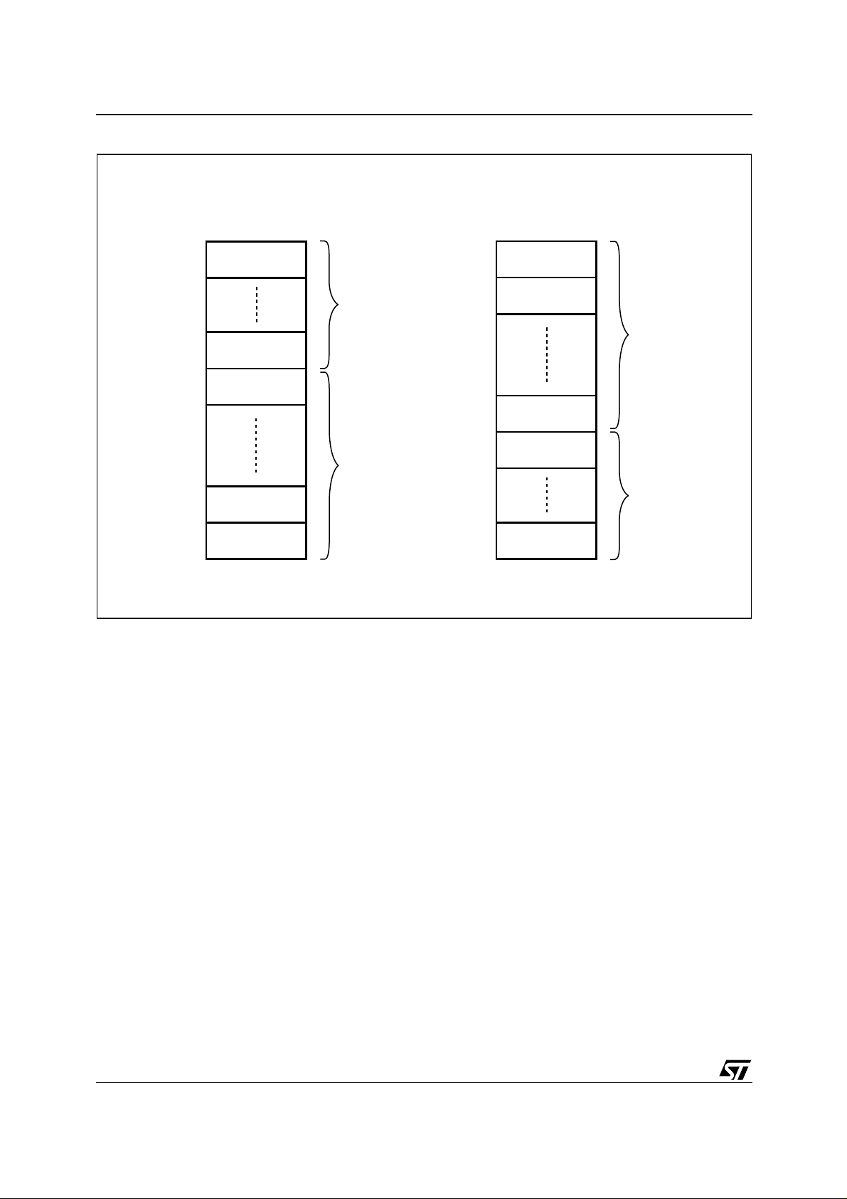
The device features an asymmetrical blocked ar-
chitecture. The M28W320EB has an array of 71
blocks: 8 Parameter Blocks of 4 KWord and 63
Main Blocks of 32 KWord. M28W320EBT has the
Parameter Blocks at the top of the memory address space while the M28W320EBB locates the
Parameter Blocks starting from the bottom. The
memory maps are shown in Figure 5, Block Addresses.
Parameter blocks 0 and 1 can be protected from
accidental programming or erasure. Each block
can be erased separately. Erase can be suspended in order to perform either read or program in
any other block and then resumed . Program can
be suspended to read data in any other block and
then resumed. Each block can be programmed
and erased over 100,000 cycles.
Program and Erase command s are written to the
Command Interface of the memory. An on-chip
Program/Erase Controller takes care of the timings necessary for program and erase operations.
The end of a program or erase operation can be
detected and any error conditions identified. The
command set required to control the memory is
consistent with JEDEC standards.
The memory is offered in TSOP48 (10 X 20mm),
and TFBGA47 (6.39 x 6.37mm, 0.75mm pitch)
packages and is supplied with all the bits erased
(set to ’1’).
M28W320EBT, M28W320EBB
Figure 2. Logic Diagram
V
V
DDQVPP
DD
21
A0-A20
W
E
G
RP
WP
Table 1. Signal Names
A0-A20 Address Inputs
DQ0-DQ15 Data Input/Output
E
G
W
RP
M28W320EBT
M28W320EBB
V
SS
Chip Enable
Output Enable
Write Enable
Reset
16
DQ0-DQ15
AI05514
WP
V
DD
V
DDQ
V
PP
V
SS
Write Protect
Core Power Supply
Power Supply for
Input/Output
Optional Supply Voltage for
Fast Program & Erase
Ground
5/45
M28W320EBT, M28W320EBB
Figure 3. TSOP Con necti on s
A15
A14
A13
A12
A11
1
48
A16
V
DDQ
V
SS
DQ15
DQ7
A10 DQ14
37
36
DQ6
DQ13
DQ5
DQ12
DQ4
V
DD
DQ11
DQ3
DQ10
DQ2
DQ9
DQ1
DQ8
DQ0
G
V
SS
E
A0
A9
A8
NC
A20
RP
V
PP
WP
A19
A18
A17
A7
A6
A5
A4
A3
A2
A1
W
12
M28W320EBT
M28W320EBB
13
24 25
6/45
AI05515
Figure 4. TFBGA Connections (Top view through package)
M28W320EBT, M28W320EBB
87654321
A
B
C
D
E
F
DDQ
SS
DQ7V
A8A11A13
DQ13
PP
RP A18
DQ11
DQ12
DQ4
WP A19
A20
DQ2
DD
A7V
A5A17WA10A14
DQ0DQ9DQ3DQ6DQ15V
DQ1DQ10V
A4
A2
A1A3A6A9A12A15
A0EDQ8DQ5DQ14A16
V
SS
G
AI03823
7/45
M28W320EBT, M28W320EBB
Figure 5. Block Addresses
M28W320EBT
Top Boot Block Addresses
1FFFFF
1FF000
1F8FFF
1F8000
1F7FFF
1F0000
00FFFF
008000
007FFF
000000
4 KWords
4 KWords
32 KWords
32 KWords
32 KWords
Total of 8
4 KWord Blocks
Total of 63
32 KWord Blocks
M28W320EBB
Bottom Boot Block Addresses
1FFFFF
1F8000
1F7FFF
1F0000
00FFFF
008000
007FFF
007000
000FFF
000000
32 KWords
32 KWords
32 KWords
4 KWords
4 KWords
Total of 63
32 KWord Blocks
Total of 8
4 KWord Blocks
AI05516
Note: Also see Appendix A, Tables 21 and 22 f or a full listing of the Block A ddresses.
8/45

SIGNAL DESCRIPTIONS
See Figure 2 Logic Diagram and T able 1,Signal
Names, for a brief overview of the signals connected to this de vice.
Address Inputs (A0-A20). The Address Inputs
select the cell s in th e memory array to a ccess during Bus Read operations. During Bus Write operations they control the commands sent to the
Command Interface of the internal state machine.
Data Input/Output (DQ0-DQ15). The Data I/O
outputs the data stored at the selected address
during a Bus Read operation or inputs a command
or data to be programmed during a Write Bus operation.
Chip Enable (E
). The Chip Enable input acti-
vates the memory control logic, input bu ffers, decoders and sense amplifiers. When Chip Enable is
and Reset is at VIH the device is in active
at V
IL
mode. When Chi p E nable is at V
the memory is
IH
deselected, the outputs are high impedan ce and
the power consumption is reduced to the stand-by
level.
Output Enable (G
). The Output Enable controls
data outputs during the Bus Read operation of the
memory.
Write Enable (W
). The Write Enable controls the
Bus Write operation of the memory’s Command
Interface. The data and address inputs are latched
on the rising edge of Chip Enable, E, or Write Enable, W
Write Protect (WP
, whichever occurs first.
). Write Protect is an input to
protect or unprotect the two lockable parameter
blocks. When Write Protect is at V
, the lockable
IL
blocks are protected and Program or Erase operations are not possible. When Wr ite Protect is at
, the lockable blocks are unprotected and can
V
IH
be programmed or erased (refer to Table 5, Memory Blocks Protect ion Truth).
Reset (RP
ware reset of the memory. W hen Reset is at V
). The Reset input provides a hard-
IL
the memory is in reset mode: the outputs are high
impedance and the current consumption is minimized. When Reset is at V
, the device is in nor-
IH
M28W320EBT, M28W320EBB
mal operation. Exiting reset mode the device
enters read array mode, but a negative trans ition
of Chip Enable or a change of the address is required to ensure valid data outputs.
V
Supply Voltage. VDD provides the power
DD
supply to the internal core of the memory device.
It is the main power supply for all operations
(Read, Program and Erase).
Su pp ly V olt ag e . V
V
DDQ
power supply to the I/O pins a nd ena bles all Outputs to be powered independently from V
can be tied to VDD or can use a separate supply.
V
Program Supply Voltage. VPP is both a
PP
control input and a power supply pin. The two
functions are selected by the voltage range applied to the pin. The Supply Voltage V
Program Supply Voltage V
any order.
If V
is kept in a low voltage range (0V to 3.6V)
PP
V
is seen as a control input. In this case a volt-
PP
age lower than V
gives an absolute protection
PPLK
against program or erase, whi le V
ables these functions (see Table 12, DC Characteristics for the relevant values). V
sampled at the beginning of a Program or Erase;
a change in its value after the operation has started does not have any effect on Program or Erase,
however for Double or Q uadruple Word Program
the results are uncertain.
is in the range 11.4V to 12.6V it acts as a
If V
PP
power supply pin. In t his condition V
stable until the Program/Erase algorithm i s completed (see Table 14 and 15).
Ground. VSS is the reference for all voltage
V
SS
measurements.
Note: Each device in a system should have
V
DD,VDDQ
and VPP decoupled with a 0.1µF ca-
pacitor close to the pin. See Figure 7, AC Mea-
,
surement Load Circu it. The PCB trace widths
should be sufficient to carry the required V
Program and Erase currents.
provides the
DDQ
can be applied in
PP
PP
DD
and the
DD
> V
is only
PP
must be
PP
. V
PP1
DDQ
en-
PP
9/45
M28W320EBT, M28W320EBB
BUS OPERATIONS
There are six standard bus operations that control
the device. These are Bus Read, Bus Wri te, Output Disable, Standby, Automatic Standby and Reset. See Table 2, Bus Operations, for a summary.
Typically glitches of less than 5ns on Chip Enable
or Write Enable are ignored by the memory and do
not affect bus operations.
Read. Read Bus operations are used to output
the contents of the Memory Array, the Electronic
Signature, the Status Register and the Common
Flash Interface. Both Chip Enable and Output Enable must be at V
eration. The Chip Enable input should be used t o
enable the device. Out put E nable shoul d be used
to gate data onto th e output. The data read depends on the previous command written to the
memory (see Command Interface section). See
Figure 8, Read Mode AC Wa veforms, and Table
13, Read AC Characteristics, for details of when
the output becomes valid.
Read mode is the default state of the device when
exiting Reset or after power-up.
Write. Bus Write operations write Comm ands to
the memory or latch Input Data to be programmed.
A write operation is initiated when Chip Enable
and Write Enable are at V
V
. Commands, Input Data and Addresses are
IH
latched on the rising edge of Write Enable or Chip
Enable, whichever occurs first.
in order to perform a read op-
IL
with Output Enable at
IL
See Figures 9 and 10, Write AC Waveforms, and
Tables 14 and 15, Write AC Characteristics, for
details of the timing requirements.
Output Disa bl e . The data outputs are high impedance when the Output Enable is at V
.
IH
Standby. Stan dby disables most of the inte rnal
circuitry allowing a substantial reduction of the current consumption. The memory is in stand-by
when Chip Enable is at V
and the device is in
IH
read mode. The power consumption is reduced to
the stand-by level and the o utputs are set to high
impedance, independently from the Output Enable
or Write Enable inputs. If Chip Enable switches to
V
during a program or erase operation, t he de-
IH
vice enters Standby mode when finished.
Automatic Standby. Automatic Standby pro-
vides a low power consumption state during Read
mode. Following a read operation, the device enters Automatic Standby after 150ns of bus inactivity, even if Chip Enable is low, V
current is reduced to I
. The data I nputs/Out-
DD1
, and the supply
IL
puts will st ill ou t p ut d ata.
Reset. During Reset mode, when Output Enable
is low, V
, the memory is deselected and the out-
IL
puts are high impedance. The memory is in Reset
mode when Reset is at V
. The power consump-
IL
tion is reduced to the Standby level, independently
from the Chip Enable, Output Enable or Write Enable inputs. If Reset is pulled to V
during a Pro-
SS
gram or Erase, this operation is aborted and the
memory content is no longer valid.
Table 2. Bus Operations
Operation E G W RP WP
Read
Write
Output Disable
Standby
Reset X X X
Note: X = VIL or VIH, V
10/45
V
V
V
V
= 12V ± 5%.
PPH
IL
IL
IL
IH
V
IL
V
IH
V
IH
XX
V
IH
V
IL
V
IH
V
IH
V
IH
V
IH
V
IH
V
IL
V
PP
X Don’t Care Data Output
V
X
X Don’t Care Hi-Z
X Don’t Care Hi-Z
X Don’t Care Hi-Z
DD
or V
PPH
DQ0-DQ15
Data Input
COMMAND INTERFACE
All Bus Write operations t o the me mory are in terpreted by the Command Interface. Commands
consist of one or more sequential Bus Write operations. An internal Program/Erase Controller handles all timings and verifies the correct execution
of the Program and Erase commands. The Program/Erase Controller provides a Status Regi ster
whose output may be read at any time, to monitor
the progress of an operation, or the Program/
Erase states. See T able 3, Command Codes , for
a summary of the commands and see Appendix D,
Table 29, Write State Machine Current/Next, for a
summary of the Command Interface.
The Command Interface is reset to Read mode
when power is first applied, when exiting from Reset or whenever V
is lower than V
DD
LKO
. Command sequences must be followed exactly. Any
invalid combination of commands will reset the device to Read mode. Refer to Table 4, Commands,
in conjunction with the text descriptions below.
Read Memory Array command
The Read command returns the memory to its
Read mode. One Bus Write cycle is required to issue the Read Memory Array command and return
the memory to Read mode. Subsequ ent read operations will read the addressed location and output the data. When a device Reset occurs, the
memory defaults to Read mode.
Read Status Register Command
The Status Register indicates when a program or
erase operation is complete and the success or
failure of the operation itself. Issue a Read Status
Register command to rea d the Status Register’s
contents. Subsequent Bus Read op erations read
the Status Register, at any addres s, until anot her
command is issued. See Tab le 8, Status Register
Bits, for details on the definitions of the bits.
The Read Status Register command m ay be issued at any time, even during a Program/Erase
operation. Any Read attempt during a Program/
Erase operation will automatically output the content of the Status Register.
Read Electronic Signature Command
The Read Electronic Signature command reads
the Manufacturer and Device Codes.
The Read Electronic Signature command consists
of one write cycle, a subsequent read will ou tput
the Manufacturer or the Device Code depending
on the levels of A0. The Manufacturer Code is output when the address line A0 is at V
Code is output when A 0 is at V
A7 must be kept to V
, other addresses are ig-
IL
, the Device
IL
. Addresses A1-
IH
nored. The codes are output on DQ0-DQ7 with
DQ8-DQ15 at 00h. (see Table 5)
M28W320EBT, M28W320EBB
Table 3. Command Codes
Hex Code Command
10h Program
20h Erase
30h
40h Program
50h Clear Status Register
55h Reserved
56h
70h Read Status Register
90h Read Electronic Signature
98h Read CFI Query
B0h Program/Erase Suspend
D0h Program/Erase Resume
FFh Read Memory Array
Read CFI Query Command
The Read Query Command is used to read dat a
from the Common Flash Interface (CFI) Me mory
Area, allowing programming equi pment or applications to automatically match their interface to
the characteristics of the device.
One Bus Write cycle is required to issue the Read
Query Command. Once the command is issued
subsequent Bus Read operations read from the
Common Flash Interfac e Memory Area. See Appendix B, Common Flash Interface, Tables 23, 24,
25, 26, 27 and 28 for details on the information
contained in the Common Flash Interface memory
area.
Block Erase Command
The Block Erase com mand can be used to erase
a block. It sets all the bits within the selected block
to ’1’. A ll previous data in t he block is lost. If the
block is protected then the Erase operation will
abort, the data in the block will not be changed and
the Status Register will output the error.
Two Bus Write cycles are required to issue the
command.
■ The first bus cycle sets up the Erase command.
■ The second latches the block address in the
internal state machine and starts the Program/
Erase Controller.
If the second bus cycle is not Write Erase Confirm
(D0h), Status Register bits b4 and b5 are set and
the command aborts.
Double Word Program
Quadruple Word Program
11/45

M28W320EBT, M28W320EBB
Erase aborts if Reset turns to VIL. As data integrity
cannot be guaranteed when the Erase operation is
aborted, the block must be erased again.
During Erase operations the memory will onl y accept the Read Status Register command and the
Program/Erase Suspend command, all other commands will be ignored. Typical Erase times are
given in Table 7, Program, Erase Times and Pr ogram/Erase Endurance Cycles.
See Appendix C , Figure 20, Erase Fl owchart and
Pseudo Code, for the flowchart for using the Erase
command.
Program Command
The memory array can be programmed word-byword. Two bus write cycles are required to issue
the Program command.
■ The first bus cycle sets up the Program
command.
■ The second latches the Address and the Data to
be written and starts the Program/Erase
Controller.
During Program operations the memory will only
accept the Read Status Register command and
the Program/Erase Su spend command. All ot her
commands will be ignored. Typical Program times
are given in Table 7, Prog ram, Erase Times and
Program/Erase Endurance Cycles.
Programming aborts if Reset goe s to V
. As data
IL
integrity cannot be guaranteed when the program
operation is aborted, the block containing the
memory location must be erased and reprogrammed.
See Appendix C, Figure 16, Program Flowchart
and Pseudo Code, for the f lowchart for using the
Program command.
Double Word Program Command
This feature is offered to improve the programming
throughput, writing a page of two adjacent words
in parallel.The two words m ust differ only for the
address A0. Programm ing s hould not b e at t emp ted when V
is not at V
PP
PPH
.
Three bus write cycles are necessary to issue the
Double Word Program command.
■ The first bus cycle sets up the Double Word
Program command.
■ The second bus cycle latches the Address and
the Data of the first word to be written.
■ The third bus cycle latches the Address and the
Data of the second word to be written and starts
the Program/Erase Controller.
Read operations output the Status Register content after the programming has s tarted. Programming aborts if Res et goes to V
. As data integrity
IL
cannot be guaranteed when the program opera-
tion is aborted, the block containing the memory
location must be erased and reprogrammed.
See Appendix C, Figure 17, Double Word Program Flowchart and Pseudo Code, for the flowchart for using the Double Word Program
command.
Quadruple Word Program Command
This feature is offered to improve the programming
throughput, writing a page of four adjacent words
in parallel.The four words must differ only for the
addresses A0 and A1. Programming should not be
attempted when V
is not at V
PP
PPH
.
Five bus write cycles are necessary to issue the
Quadruple Word Program command.
■ The first bus cycle sets up the Quadruple Word
Program Command.
■ The second bus cycle latches the Address and
the Data of the first word to be written.
■ The third bus cycle latches the Address and the
Data of the second word to be written.
■ The fourth bus cycle latches the Address and
the Data of the third word to be written.
■ The fifth bus cycle latches the Ad dr es s and th e
Data of the fourth word to be written and starts
the Program/Erase Controller.
Read operations output the Status Register content after the programming has s tarted. Programming aborts if Reset goes to V
. As data integrity
IL
cannot be guaranteed when the program operation is aborted, the block containing the memory
location must be erased and reprogrammed.
See Appendix C, Figure 18, Quadruple Word Program Flowchart and Pseudo Code, for the flowchart for using the Quadruple Word Program
command.
Clear Status Register Command
The Clear Status Register comm and can be used
to reset bits 1, 3, 4 and 5 in the Status Register to
‘0’. One bus write cycle is required to issue the
Clear Status Register command.
The bits in the Status Register do not automatically return to ‘0’ when a new Program or Erase command is issued. The error bits in the Status
Register should be cleared before attempting a
new Program or Erase command.
Program/Erase Suspend Command
The Program/Erase Suspend command is used to
pause a Program or Erase operation. One bus
write cycle is required to issue the Program/Erase
command and pau se the Prog ram/Erase controller.
During Program/Erase Suspend the Command Interface will accept the Program/Erase Resume,
Read Array, Read Status Register, Read Electronic Signature and Read CFI Query commands. Ad-
12/45

M28W320EBT, M28W320EBB
ditionally, if the suspend operation was Erase then
the Program, Double Wo rd P rogram and Q uadruple Word Program commands will also be accepted. Only the blocks no t be i ng era se d may be read
or programmed correctly.
During a Program/Erase Suspend, the device can
be placed in a pseudo-standby mode by taking
Chip Ena ble to V
Reset turns to V
. Program/Erase is aborted if
IH
.
IL
See Appendix C, Figure 19 , Program Suspend &
Resume Flowchart and Pseudo Code, and Figure
21, Erase Suspend & Resume Flowchart and
Pseudo Code for flowcharts for using the Program/
Erase Suspend command.
Program/Erase Resume Command
The Program/Erase Resume command can be
used to restart the Program/Erase Controller after
a Program/Erase Suspend o peration has paused
it. One Bus Write cycle is required to issue the
command. Once the command is issued subse-
quent Bus Read operations read the Status Register.
See Appendix C, Figure 19, Program or Double
Word Program Suspend & Resume Flowchart and
Pseudo Code, an d Figure 21, Erase Sus pend &
Resume Flowchart and Pseudo Code for flowcharts for using the Program/Erase Resume command.
Block Protection
Two parameter/lockable blocks (blocks #0 and #1)
can be protected against Program or Erase operations. Unprotect ed blocks ca n be progra mmed or
erased.
To protect the two lockab le blocks set W rite Protect to V
. When VPP is below V
IL
all blocks are
PPLK
protected. Any attempt to Program or Erase protected blocks will abort, the data in the block will
not be changed and t he Status Register outputs
the error.
Table 6, Memory Blocks P rotection Truth Table,
defines the protection methods.
13/45
M28W320EBT, M28W320EBB
Table 4. Commands
Commands
No. of
Cycles
1st Cycle 2nd Cycle 3nd Cycle
Bus
Op.
Addr Data
Bus Write Operations
Bus
Addr Data
Op.
Bus
Op.
Addr Data
Read Memory Array Write X FFh
Read Status
Register
Read Electronic
Signature
Read CFI Query Write X 98h Read QA QD
Erase Write X 20h Write BA D0h
Program Write X
Double Word
Program
Quadruple Word
Program
Clear Status
Register
Program/Erase
Suspend
Program/Erase
Resume
Note: 1. X = Don’t C are, RA=Rea d Addre ss, RD =Read D ata, SRD =Stat us Regis ter Da ta, ID =Identif ier (Ma nufact ure and Devic e Code),
(3)
(4)
QA=Query Address, QD=Query Data, BA=Block Address, PA=Program Address, PD=Program Data, PRA=Protection Register Address, PRD=Protection Regis ter Data.
2. A0 =V
3. Program Addres ses 1 and 2 must be consecuti ve Addresses differing only for A0.
4. Program Addres ses 1,2,3 and 4 m ust be consecutive Addresses differing only for A0 and A1.
5. 55h is reserved.
6. To be c haracteriz ed.
outputs Manufacturer code, A0=VIHoutputs Device code. A ddress A7-A1 must be VIL.
IL
Write X 70h Read X SRD
Write X 90h Read
40h or
Write X 30h Write PA1 PD1 Write PA2 PD2
Write X
Write X 50h
Write X B0h
Write X D0h
56h
Read
Write PA PD
10h
(6)
Write PA1 PD1 Write PA2 PD2 Write PA3 PD3 Write
RA RD
(2)
SA
IDh
Table 5. Read Electronic Signature
Code Device E G W A0 A1-A7 A8-A20 DQ0-DQ7 DQ8-DQ15
Manufacture.
Code
M28W320EBT
Device Code
M28W320EBB
Note: RP = VIH.
14/45
V
V
V
IL
IL
V
V
IL
IL
V
V
IL
IL
V
IH
V
V
IH
V
V
IH
V
IL
V
IH
V
IH
Don’t Care 20h 00h
IL
Don’t Care BCh 88h
IL
Don’t Care BDh 88h
IL

M28W320EBT, M28W320EBB
Table 6. Memory Blocks Protection Truth Table
(1)
V
PP
X
V
IL
V
or V
DD
V
or V
DD
Note: 1 . X = Don’t Care
2. V
(2)
PPH
(2)
PPH
must also be greater than the Program Voltage Lock Out V
PP
RP WP
V
IL
V
IH
V
IH
V
IH
(1)
X Protected Protected
X Protected Protected
V
IL
V
IH
Table 7. Program, Erase Tim es and Pro gra m /Erase Endurance Cycle s
Parameter Test Conditions
V
Word Program
Double Word Program
Quadruple Word Program
Main Block Program
Parameter Block Program
Main Block Erase
Parameter Block Erase
Program/Erase Cycles (per Block) 100,000 cycles
Note: 1. Typical time to program a Main or Parameter Block using the Double Word Program and the Quadruple Word Program commands
respectively.
= V
PP
V
= 12V ±5%
PP
V
= 12V ±5%
PP
V
= 12V ±5%
PP
= V
V
PP
V
= 12V ±5%
PP
= V
V
PP
V
= 12V ±5%
PP
V
= V
PP
V
= 12V ±5%
PP
= V
V
PP
DD
DD
DD
DD
DD
Lockable Blocks
(blocks #0 and #1)
Other Blocks
Protected Unprotected
Unprotected Unprotected
.
PPLK
M28W320EB
Min Typ Max
10 200 µs
10 200 µs
10 200 µs
0.16/0.08
(1)
5s
0.32 5 s
0.02/0.01
(1)
4s
0.04 4 s
110s
110s
0.4 10 s
0.4 10 s
Unit
15/45

M28W320EBT, M28W320EBB
STATUS REGISTER
The Status Register provides information on t he
current or previous Program or Erase operation.
The various bits convey information and errors on
the operation. To read the Status register the
Read Status Register command can be issued, refer to the Read Status Register Command section.
To output the contents, the Status Register is
latched o n the falling edge of the Ch ip Enable or
Output Enable signals, and can be read until Chip
Enable or Output Enable returns to V
. Either
IH
Chip Enable or Output Enable must be toggled to
update the latched data.
Bus Read operations from any address always
read the Status Register during Program and
Erase operations.
The bits in the Status Register are summarized in
Table 8, Status Register Bits. Refer to Table 8 in
conjunction with the following text descriptions.
Program/Erase Controller Status (Bit 7). The Progra m/Erase Controller Status bit indicates whether
the Program/Erase Controller is active or inactive.
When the Program/Erase Controller Status bit is
Low (set to ‘0’), the Program/Erase Controller is
active; when the bit is High (set to ‘1’), the Program/Erase Controller is inactive, and the device
is ready to process a new command.
The Program/Erase Controller Status is Low immediately after a Program/Erase Suspend command is issued until the Program/Erase Controller
pauses. After the Program/Erase Controller pauses the bit is High .
During Program, Erase, operations the Program/
Erase Controller Status bit can be polled to find the
end of the operation. Other bits in the Status Register should not be tested until the Program/Erase
Controller completes the operation and the bit is
High.
After the Program/Erase Cont roller completes its
operation the Erase Status, Prog ram Status, V
PP
Status and Block Pr otec tion Sta tus b its should be
tested for errors.
Erase Suspend Status (Bit 6). The Erase Suspend Status bit (set to ‘1’) indicates that an Erase
operation has been suspend ed or is going to be
suspended.
The Erase Suspend Status should only be considered valid when the Program/Erase Controller Status bit is High (Program/Erase Controller inactive).
Bit 7 is set within 30µs of the Program/Erase Suspend command being issued therefore the memory may still complete the operation rather than
entering the Suspend mode.
When a Program/Erase Re sume command is issued the Erase Suspend Status bit returns Low.
memory may still complete the operation rather than entering the Suspend mode.
Erase Status (Bit 5). The Erase Status bit can be
used to identify if the memory has failed to verify
that the block has erased correctly. When the
Erase Status bit is High (set t o ‘1’), the Program/
Erase Controller has applied the max imum number of pulses to the block and still failed to verify
that the block has erased correctly. The Erase Status bit should be read once the Program/Erase
Controller Status bit is High (Program/Erase Controller inactive).
Once set High, the Erase Status bit can only be reset Low by a Clear Status Register command or a
hardware reset. If set High it should be reset before a new Program or Erase command is issued,
otherwise the new command will appear to fail.
Program Status (Bit 4). The Program Status bit
is used to identify a Program failure. When the
Program Status bit is High (set to ‘1’), the Program/Erase Controller has applied the maximum
number of pulses to the byte and still failed to verify that it has programmed correctly. The Program
Status bit should be read once the Program/Erase
Controller Status bit is High (Program/Erase Controller inactive).
Once set High, the Program Status bit can only be
reset Low by a Clear Status Register command or
a hardware reset. If set High it should be reset before a new command is issued, otherwise the new
command will appear to fail.
V
Status (Bit 3). The VPP Status bit can be
PP
used to identify an invalid volt age on the V
during Program and Erase operations. The V
PP
pin
PP
pin is only sampled at the beginning of a Program
or Erase operation. Indeterminate results can occur if V
When the V
age on the V
when the V
becomes invalid during an operation.
PP
Status bit is Low (set to ‘0’), the volt-
PP
pin was sampled at a valid voltage;
PP
Status bit is High (set to ‘1’), the V
PP
PP
pin has a voltage that is below the VPP Lockout
Voltage, V
, the memory is protected and Pro-
PPLK
gram and Erase operations cannot be performed.
Once set High, the V
Status bit can only be reset
PP
Low by a Clear Status Register command or a
hardware reset. If set High it should be reset before a new Program or Erase command is issued,
otherwise the new command will appear to fail.
Program Suspend Status (Bit 2). The Program
Suspend Status bit (set to ‘1’) indicates that a Program operation has been suspended or is going to
be suspended.
The Program Suspend Status should only be considered valid when the Program/Erase Controller
Status bit is High (Program/Erase Con troller inactive). Bit 2 is set within 5µs of the Program/Erase
Suspend command being issued therefore the
16/45

M28W320EBT, M28W320EBB
When a Program/Erase Re sume command is issued the Program Suspend Status bit returns Low.
Block Protection Status (Bit 1). The Block Protection Status bit can be used to identify if a Program or Erase operation has tried to modify the
contents of a protected block.
When the Block Protection S tatus bit is High (set
to ‘1’), a Program or Erase operation has been attempted on a protected block.
Once set High, the Block Protection Status bit can
only be reset Low by a Clear Status Register command or a hardware reset. If set High it should be
reset before a new command is issued, otherwise
the new command will appear to fail.
Reserved (Bit 0). Bit 0 of the Status Register is
reserved. Its value must be masked.
Note: Refer to Appendix C, Flowcharts and
Pseudo Codes, for using the Status Register.
Table 8. Status Register Bits
Bit Name Logic Level Definition
7 P/E.C. Status
6 Erase Suspend Status
5 Erase Status
4 Program Status
Status
3
2 Program Suspend Status
V
PP
’1’ Ready
’0’ Busy
’1’ Suspended
’0’ In progress or Completed
’1’ Erase Error
’0’ Erase Success
’1’ Program Error
’0’ Program Success
V
’1’
’0’
’1’ Suspended
’0’ In Progress or Completed
Invalid, Abort
PP
OK
V
PP
1 Block Protection Status
0 Reserved
Note: Logic level ’1’ is High, ’0’ is Low.
’1’ Program/Erase on protected Block, Abort
’0’ No operation to protected blocks
17/45

M28W320EBT, M28W320EBB
MAXIMUM RATIN G
Stressing the device above the rating l isted in the
Absolute Maximum Ratings table m ay cause permanent damage to the device. Exposure to Absolute Maximum Rating conditions for extended
periods may affect device reliability. These are
stress ratings only and operation of the dev ice at
Table 9. Absolute Maximum Ratings
Symbol Parameter
T
A
T
BIAS
T
STG
V
IO
V
, V
DD
DDQ
V
PP
Note: 1. Depends on range.
Ambient Operating Temperature
Temperature Under Bias –40 125 °C
Storage Te mperat ure –55 155 °C
Input or Output Voltage –0.6
Supply Voltage –0.6 4.1 V
Program Voltage –0.6 13 V
(1)
these or any other conditions above those indicated in the Operating sections of this specification is
not implied. Refer also to the STMicroelectronics
SURE Program and other relevan t quality documents.
Value
Min Max
–40 85 °C
V
+0.6
DDQ
Unit
V
18/45

DC AND AC PARAMETERS
This section summarizes the operat ing and measurement conditions, and the DC and AC characteristics of the device. The parameters in the DC
and AC characteristics Tables that follow, are derived from tests performed under the Measure-
ment Conditions summarized in Table 10,
Operating and AC Measurem ent Conditions. Designers should check that the operating conditions
in their circuit match the measurement conditions
when relying on the quoted parameters.
Table 10. Operating and AC Measurement Conditions
M28W320EBT, M28W320EBB
M28W320EBT, M28W320EBB
Parameter
70 85 90 1 00
Min Max Min Max Min Max M in Max
V
Supply Voltage
DD
V
Supply Voltage (V
DDQ
DDQ
≤ V
DD
2.7 3.6 2.7 3.6 2.7 3.6 2.7 3.6 V
2.7 3.6 2.7 3.6 2.7 3.6 1.65 3.6 V
)
Ambient Operating T emperature – 40 85 – 40 85 – 40 85 – 40 85 °C
Load Capacitance (C
)
L
50 50 50 50 pF
Input Rise and Fall Times 5 5 5 5 ns
Input Pulse Voltages
Input and Output Timing Ref.
Voltages
0 to V
V
DDQ
DDQ
/2 V
0 to V
DDQ
DDQ
/2 V
0 to V
DDQ
DDQ
/2 V
0 to V
DDQ
DDQ
/2
Figure 6. AC Measurement I/O Waveform Figu re 7. AC Measurement Loa d Circuit
V
DDQ
V
DDQ
V
/2
DDQ
0V
AI00610
V
DDQ
V
DD
25kΩ
Units
V
V
DEVICE
UNDER
TEST
0.1µF
0.1µF
CL includes JIG capacitance
C
Table 11. Device Capacitance
Symbol Parameter Test Condition Min Max Unit
V
V
IN
OUT
= 0V
= 0V
6pF
12 pF
C
IN
C
OUT
Note: Sampled o nl y, not 100% test ed.
Input Capacitance
Output Capacitance
L
25kΩ
AI00609C
19/45

M28W320EBT, M28W320EBB
Table 12. DC Characteristics
Symbol Parameter Test Condition Min Typ Max Unit
I
LI
I
LO
I
DD
I
DD1
I
DD2
I
DD3
I
DD4
I
DD5
I
PP
I
PP1
I
PP2
I
PP3
I
PP4
V
IL
V
IH
V
OL
V
OH
V
PP1
V
PPH
V
PPLK
V
LKO
Input Leakage Current
Output Leakage Current
Supply Current (Read)
Supply Current (Stand-by or
Automatic Stand-by)
Supply Current
(Reset)
Supply Current (Program)
Supply Current (Erase)
Supply Current
(Program/Erase Suspend)
Program Current
(Read or Stand-by)
Program Current
(Read or Stand-by)
Program Current (Reset)
Program Current (Program)
Program Current (Erase)
Input Low Voltage
Input High Voltage
Output Low Voltage
Output High Voltage
Program Voltage (Program or
Erase operations)
Program Voltage
(Program or Erase
operations)
Program Voltage
(Program and Erase lock-out)
VDD Supply Voltage (Program
and Erase lock-out)
0V≤ V
0V
E
= VSS, G = VIH, f = 5MHz
= V
E
RP
= V
RP
Program in progress
V
PP
Program in progress
Erase in progress
V
PP
Erase in progress
E
= V
Erase suspended
RP
Program in progress
V
PP
Program in progress
Erase in progress
V
PP
Erase in progress
V
V
I
= 100µA, VDD = VDDmin,
OL
V
DDQ
I
= –100µA, VDD = VDDmin,
OH
V
DDQ
V
≤
IN
DDQ
V
OUT
DDQ
DDQ
V
≤
DDQ
± 0.2V,
± 0.2V
≤
= VSS ± 0.2V
= 12V ± 5%
V
= V
PP
DD
= 12V ± 5%
V
= V
PP
DD
± 0.2V,
DDQ
> V
V
PP
DD
V
≤
V
PP
DD
= VSS ± 0.2V
= 12V ± 5%
= V
V
PP
DD
= 12V ± 5%
= V
V
PP
DD
2.7V
≥
DDQ
2.7V 0.7 V
≥
DDQ
= V
= V
DDQ
DDQ
min
min
±1 µA
±10 µA
918mA
15 50 µA
15 50 µA
510mA
10 20 mA
520mA
10 20 mA
15 50 µA
400 µA
15µA
15µA
110mA
15µA
310mA
15µA
–0.5 0.4 V
–0.5 0.8 V
V
–0.4 V
DDQ
DDQ
V
DDQ
DDQ
+0.4
+0.4
0.1 V
–0.1
V
DDQ
1.65 3.6 V
11.4 12.6 V
1V
2V
V
V
V
20/45

Figure 8. Read AC Waveforms
M28W320EBT, M28W320EBB
tAVAV
A0-A20
tAVQV
E
tELQX
G
tGLQX
DQ0-DQ15
ADDR. VALID
CHIP ENABLE
Table 13. Read AC Characteristics
Symbol Alt Parameter
t
AVAV
t
AVQV
t
AXQX
t
EHQX
t
EHQZ
t
ELQV
t
ELQX
t
GHQX
t
GHQZ
t
GLQV
t
GLQX
Note: 1. Sampled only, not 100% tested.
2. G
t
Address Valid to Next Address Valid Min 70 85 90 100 ns
RC
t
Address Valid to Output Valid Max 70 85 90 100 ns
ACC
(1)
t
Address Transition to Output Transition Min 0 0 0 0 ns
OH
(1)
t
Chip Enable High to Output Transition Min 0 0 0 0 ns
OH
(1)
t
Chip Enable High to Output Hi-Z Max 20 20 25 30 ns
HZ
(2)
t
Chip Enable Low to Output Valid Max 70 85 90 100 ns
CE
(1)
t
Chip Enable Low to Output Transition Min 0 0 0 0 ns
LZ
(1)
t
Output Enable High to Output Transition Min 0 0 0 0 ns
OH
(1)
t
Output Enable High to Output Hi-Z Max 20 20 25 30 ns
DF
(2)
t
Output Enable Low to Output Valid Max 20 20 30 35 ns
OE
(1)
t
Output Enable Low to Output Transition Min 0 0 0 0 ns
OLZ
may be delayed by up to t
ELQV
- t
after the fal ling edge of E without increasing t
GLQV
tELQV
tGLQV
OUTPUTS
ENABLED
VALID
tEHQX
tEHQZ
tGHQX
tGHQZ
VALID
DATA VALID STANDBY
M28W320EB
70 85 90 10
.
ELQV
tAXQX
AI03825b
Unit
21/45

M28W320EBT, M28W320EBB
Figure 9. Write AC Waveforms, Write Enable Controlled
AI03826b
tWHAX
PROGRAM OR ERASE
tAVAV
VALIDA0-A20
tAVWH
tWHGL
tELQV
tWHEL
tQVWPL
STATUS REGISTER
tQVVPL
READ
1st POLLING
STATUS REGISTER
OR DATA INPUT
22/45
E
tELWL tWHEH
WP
tVPHWH
PP
V
SET-UP COMMAND CONFIRM COMMAND
tWPHWH
tWHWL
G
W
tWHDX
tWLWH
tDVWH
DQ0-DQ15 COMMAND CMD or DATA

Table 14. Write AC Characteristics, Write Enable Controlled
Symbol Alt Parameter
M28W320EBT, M28W320EBB
M28W320EB
Unit
70 85 90 10
t
AVAV
t
AVWH
t
DVWH
t
ELWL
t
ELQV
(1,2)
t
QVVPL
t
QVWPL
t
VPHWH
t
WHAX
t
WHDX
t
WHEH
t
WHEL
t
WHGL
t
WHWL
t
WLWH
t
WPHWH
Note: 1. Sampled only, not 100% tested.
2. Appl i cable if V
(1)
t
Write Cycle Time Min 70 85 90 100 ns
WC
t
Address Valid to Write Enable High Min 45 45 50 50 ns
AS
t
Data Valid to Write Enable High Min 45 45 50 50 ns
DS
t
Chip Enable Low to Write Enable Low Min 0 0 0 0 ns
CS
Chip Enable Low to Output Valid Min 70 85 90 100 ns
Output Valid to VPP Low
Output Valid to Write Protect Low Min 0 0 0 0 ns
t
VPSVPP
t
AH
t
DH
t
CH
High to Write Enable High
Write Enable High to Address Transition Min 0 0 0 0 ns
Write Enable High to Data Transition Min 0 0 0 0 ns
Write Enable High to Chip Enable High Min 0 0 0 0 ns
Write Enable High to Chip Enable Low Min 25 25 30 30 ns
Write Enable High to Output Enable Low Min 20 20 30 30 ns
t
Write Enable High to Write Enable Low Min 25 25 30 30 ns
WPH
t
Write Enable Low to Write Enable High Min 45 45 50 50 ns
WP
Write Protect High to Write Enable High Min 45 45 50 50 ns
is seen as a logic i nput (VPP < 3.6V ).
PP
Min 0 0 0 0 ns
Min 200 200 200 200 ns
23/45

M28W320EBT, M28W320EBB
Figure 10. Write AC Waveforms, Chip Enable Controlled
AI033827b
tEHAX
PROGRAM OR ERASE
tAVAV
VALIDA0-A20
tAVEH
tEHGL
tELQV
tQVWPL
CMD or DATA STATUS REGISTER
tQVVPL
READ
1st POLLING
STATUS REGISTER
OR DATA INPUT
CONFIRM COMMAND
24/45
W
tWLEL tEHWH
WP
tVPHEH
PP
V
POWER-UP AND
SET-UP COMMAND
tWPHEH
tEHEL
G
E
tEHDX
tELEH
tDVEH
DQ0-DQ15 COMMAND

Table 15. Write AC Characteristics, Chip Enable Controlled
Symbol Alt Parameter
M28W320EBT, M28W320EBB
M28W320EB
Unit
70 85 90 10
t
AVAV
t
AVEH
t
DVEH
t
EHAX
t
EHDX
t
EHEL
t
EHGL
t
EHWH
t
ELEH
t
ELQV
(1,2)
t
QVVPL
t
QVWPL
t
VPHEH
t
WLEL
t
WPHEH
Note: 1. Sampled only, not 100% tested.
2. Appl i cable if V
(1)
t
Write Cycle Time Min 70 85 90 100 ns
WC
t
Address Valid to Chip Enable High Min 45 45 50 50 ns
AS
t
Data Valid to Chip Enable High Min 45 45 50 50 ns
DS
t
Chip Enable High to Address Transition Min 0 0 0 0 ns
AH
t
Chip Enable High to Data Transition Min 0 0 0 0 ns
DH
t
Chip Enable High to Chip Enable Low Min 25 25 30 30 ns
CPH
Chip Enable High to Output Enable Low Min 25 25 30 30 ns
t
Chip Enable High to Write Enable High Min 0 0 0 0 ns
WH
t
Chip Enable Low to Chip Enable High Min 45 45 50 50 ns
CP
Chip Enable Low to Output Valid Min 70 85 90 100 ns
Output Valid to VPP Low
Data Valid to Write Protect Low Min 0 0 0 0 ns
t
VPSVPP
t
CS
High to Chip Enable High
Write Enable Low to Chip Enable Low Min 0 0 0 0 ns
Write Protect High to Chip Enable High Min 45 45 50 50 ns
is seen as a logic i nput (VPP < 3.6V ).
PP
Min 0 0 0 0 ns
Min 200 200 200 200 ns
25/45

M28W320EBT, M28W320EBB
Figure 11. Power-Up and Reset AC Waveforms
E, G
W,
RP
tPHWL
tPHEL
tPHGL
tPHWL
tPHEL
tPHGL
tVDHPH
VDD, VDDQ
Power-Up Reset
Table 16. Power-Up and Reset AC Characteristics
Symbol Parameter Test Condition
t
PHWL
t
PHEL
t
PHGL
t
PLPH
t
VDHPH
Note: 1. The devi ce Reset is possible but not guarant eed if t
2. Sampled only, not 100% tested.
3. It is im portant to ass ert RP
Reset High to Write Enable Low, Chip
Enable Low, Output Enable Low
(1,2)
Reset Low to Reset High Min 100 100 100 100 ns
(3)
Supply Voltages High to Reset High Min 50 50 50 50 µs
in order to all ow proper CPU i ni tializati on during pow er up or reset .
PLPH
During
Program
and Erase
others Min 30 30 30 30 ns
< 100ns.
tPLPH
AI03453b
M28W320EB
Unit
70 85 90 10
Min 50 50 50 50 µs
26/45

M28W320EBT, M28W320EBB
PACKAGE MECHANICAL
Figure 12. TSOP48 - 48 lead Plastic Thin Small Outline, 12 x 20mm, Package Outline
A2
1 N
e
E
B
N/2
D1
D
DIE
A
CP
C
TSOP-a
Note: Drawing is not to scale.
LA1 α
Table 17. TSOP48 - 48 lead Plastic Thin Small Outline, 12 x 20mm, Package Mechanical Data
Symbol
A 1.20 0.0472
A1 0.05 0.15 0.0020 0.0059
A2 0.95 1.05 0.0374 0.0413
B 0.17 0.27 0.0067 0.0106
C 0.10 0.2 1 0.0039 0.0083
D 19.80 20.2 0 0.7795 0.7953
D1 18.30 18.50 0.7205 0.7283
E 11.90 12.10 0.4685 0.4764
e 0.50 – – 0.01 97 – –
L 0.50 0.70 0.0 197 0.0279
α
N48 48
CP 0.10 0.0039
Typ Min Max Typ Min Max
mm inches
0° 5° 0° 5°
27/45

M28W320EBT, M28W320EBB
Figure 13. TFBGA47 6.39x6.37mm - 8x6 ball array, 0.75mm pitch, Bottom View Package Ou tline
D
FD
FE
D1
SD
SE
E1E
e
ddd
BALL "A1"
e
A
b
A2
A1
BGA-Z35
Note: Drawing is not to scale.
Table 18. TFBGA47 6.39x6.37mm - 8x6 ball array, 0.75mm pitch, Package Mechanical Data
Symbol
Typ Min Max Typ Min Max
A 1.200 0.0472
A1 0.200 0.0079
millimeters inches
A2 1.000 0.0394
b 0.400 0.350 0.450 0.0157 0.0138 0.0177
D 6.390 6.290 6.490 0.2516 0.2476 0.2555
D1 5.250 – – 0.2067 – –
ddd 0.100 0.0039
E 6.370 6.270 6.470 0.2508 0.2469 0.2547
E1 3.750 – – 0.1476 – –
e 0.750 – – 0.0295 – –
FD 0.570 – – 0.0224 – –
FE 1.310 – – 0.0516 – –
SD 0.375 – – 0.0148 – –
SE 0.375 – – 0.0148 – –
28/45

M28W320EBT, M28W320EBB
Figure 14. TFBGA47 Daisy Chain - Package Connections (Top view through package)
87654321
A
B
C
D
E
F
Figure 15. TFBGA47 Daisy Chain - PCB Connections proposal (Top view through package)
87654321
A
B
C
D
E
F
START
POINT
POINT
AI03295
END
AI03296
29/45

M28W320EBT, M28W320EBB
PART NUMBERING
Table 19. Ordering Information Scheme
Example: M28W320EBT 90 N 6 T
Device Type
M28
Operating Voltage
W = V
Device Function
320EB = 32 Mbit (x16), Boot Block
Array Matrix
T = Top Boot
B = Bottom Boot
Speed
70 = 70 ns
85 = 85 ns
90 = 90 ns
10 = 100 ns
= 2.7V to 3.6V; V
DD
= 1.65V to 3.6V
DDQ
Package
N = TSOP48: 12 x 20 mm
ZB = TFBGA47: 6.39 x 6.37mm, 0.75 mm pitch
Temperature Range
1 = 0 to 70 °C
6 = –40 to 85 °C
Option
T = Tape & Reel Packing
Table 20. Daisy Chain Ordering Scheme
Example: M28W320EB -ZB T
Device Type
M28W320EB
Daisy Chain
-ZB = TFBGA47: 6.39 x 6.37mm, 0.75 mm pitch
Option
T = Tape & Reel Packing
Note:Devices are shipped from the factory with the memory content bits erased to ’1’. For a list of available
options (Speed, Package, etc...) or for further information on any aspect of this device, please contact
the ST Sales Office nearest to you.
30/45

APPENDIX A. BLOCK ADDRESS TABLES
M28W320EBT, M28W320EBB
Table 21. Top Boot Block Addresses,
M28W320EBT
#
0 4 1FF000-1FFFFF
1 4 1FE000-1FEFFF
2 4 1FD000-1FDFFF
3 4 1FC000-1FCFFF
4 4 1FB000-1FBFFF
5 4 1FA000-1FAFFF
6 4 1F9000-1F9FFF
7 4 1F8000-1F8FFF
8 32 1F0000-1F7FFF
9 32 1E8000-1EFFFF
10 32 1E0000-1E7FFF
11 32 1D8000-1DFFFF
12 32 1D0000-1D7FFF
13 32 1C8000-1CFFFF
14 32 1C0000-1C7FFF
15 32 1B8000-1BFFFF
16 32 1B0000-1B7FFF
17 32 1A8000-1AFFFF
18 32 1A0000-1A7FFF
19 32 198000-19FFFF
20 32 190000-197FFF
21 32 188000-18FFFF
22 32 180000-187FFF
23 32 178000-17FFFF
24 32 170000-177FFF
25 32 168000-16FFFF
26 32 160000-167FFF
27 32 158000-15FFFF
28 32 150000-157FFF
29 32 148000-14FFFF
30 32 140000-147FFF
31 32 138000-13FFFF
32 32 130000-137FFF
33 32 128000-12FFFF
Size
(KWord)
Address Range
34 32 120000-127FFF
35 32 118000-11FFFF
36 32 110000-117FFF
37 32 108000-10FFFF
38 32 100000-107FFF
39 32 0F8000-0FFFFF
40 32 0F00000-F7FFF
41 32 0E8000-0EFFFF
42 32 0E0000-0E7FFF
43 32 0D8000-0DFFFF
44 32 0D0000-0D7FFF
45 32 0C8000-0CFFFF
46 32 0C0000-0C7FFF
47 32 0B8000-0BFFFF
48 32 0B0000-0B7FFF
49 32 0A8000-0AFFFF
50 32 0A0000-0A7FFF
51 32 098000-09FFFF
52 32 090000-097FFF
53 32 088000-08FFFF
54 32 080000-087FFF
55 32 078000-07FFFF
56 32 070000-077FFF
57 32 068000-06FFFF
58 32 060000-067FFF
59 32 058000-05FFFF
60 32 050000-057FFF
61 32 048000-04FFFF
62 32 040000-047FFF
63 32 038000-03FFFF
64 32 030000-037FFF
65 32 028000-02FFFF
66 32 020000-027FFF
67 32 018000-01FFFF
68 32 010000-017FFF
69 32 008000-00FFFF
70 32 000000-007FFF
31/45

M28W320EBT, M28W320EBB
Table 22. Bottom Boot Block Addresses,
M28W320EBB
#
70 32 1F8000-1FFFFF
69 32 1F0000-1F7FFF
68 32 1E8000-1EFFFF
67 32 1E0000-1E7FFF
66 32 1D8000-1DFFFF
65 32 1D0000-1D7FFF
64 32 1C8000-1CFFFF
63 32 1C0000-1C7FFF
62 32 1B8000-1BFFFF
61 32 1B0000-1B7FFF
60 32 1A8000-1AFFFF
59 32 1A0000-1A7FFF
58 32 198000-19FFFF
57 32 190000-197FFF
56 32 188000-18FFFF
55 32 180000-187FFF
54 32 178000-17FFFF
53 32 170000-177FFF
52 32 168000-16FFFF
51 32 160000-167FFF
50 32 158000-15FFFF
49 32 150000-157FFF
48 32 148000-14FFFF
47 32 140000-147FFF
46 32 138000-13FFFF
45 32 130000-137FFF
44 32 128000-12FFFF
43 32 120000-127FFF
42 32 118000-11FFFF
41 32 110000-117FFF
40 32 108000-10FFFF
39 32 100000-107FFF
38 32 0F8000-0FFFFF
37 32 0F0000-0F7FFF
Size
(KWord)
Address Range
36 32 0E8000-0EFFFF
35 32 0E0000-0E7FFF
34 32 0D8000-0DFFFF
33 32 0D0000-0D7FFF
32 32 0C8000-0CFFFF
31 32 0C0000-0C7FFF
30 32 0B8000-0BFFFF
29 32 0B0000-0B7FFF
28 32 0A8000-0AFFFF
27 32 0A0000-0A7FFF
26 32 098000-09FFFF
25 32 090000-097FFF
24 32 088000-08FFFF
23 32 080000-087FFF
22 32 078000-07FFFF
21 32 070000-077FFF
20 32 068000-06FFFF
19 32 060000-067FFF
18 32 058000-05FFFF
17 32 050000-057FFF
16 32 048000-04FFFF
15 32 040000-047FFF
14 32 038000-03FFFF
13 32 030000-037FFF
12 32 028000-02FFFF
11 32 020000-027FFF
10 32 018000-01FFFF
9 32 010000-017FFF
8 32 008000-00FFFF
7 4 007000-007FFF
6 4 006000-006FFF
5 4 005000-005FFF
4 4 004000-004FFF
3 4 003000-003FFF
2 4 002000-002FFF
1 4 001000-001FFF
0 4 000000-000FFF
32/45

M28W320EBT, M28W320EBB
APPENDIX B. COMMON FLASH INTERFACE (CFI)
The Common Flash Interface is a JEDEC approved, standardized data structure that can be
read from the Flash memory device. It allows a
system software to query the device to det ermine
various electrical and t iming parameters, density
information and functions supported by the memory. The system can interface easily with the device, enabling the software to upgrade itself when
necessary.
When the CFI Query Co mmand (RCFI) is issued
the device enters CFI Query mode and the data
Table 23. Query Structure Overview
Offset Sub-section Name Description
00h Reserved Reserved for algorithm-specific information
10h CFI Query Identification String Command set ID and algorithm data offset
1Bh System Interface Information Device timing & voltage information
27h Device Geometry Definition Flash device layout
P Primary Algorithm-specific Extended Query table
A Alternate Algorithm-specific Extended Query table
Note: Query data are always presented on the lowest order data outputs.
structure is read from the memory. Tables 23, 24,
25, 26, 27 and 28 show the addresses used to retrieve the data.
The CFI data structure also contains a security
area where a 64 bit unique security number is written (see Table 28, Security Code area). This area
can be accessed only in Read mode by the final
user. It is impossible to change the security num ber after it has been written by ST. Issue a Read
command to return to Read mode.
Additional information specific to the Primary
Algorithm (optional)
Additional information specific to the Alternate
Algorithm (optional)
Table 24. CFI Query Identification String
Offset Data Description Value
00h 0020h Manufacturer Code ST
01h
02h-0Fh reserved Reserved
10h 0051h Query Unique ASCII String "QRY" “Q”
11h 0052h Query Unique ASCII String "QRY" “R”
12h 0059h Query Unique ASCII String "QRY" “Y”
13h 0003h
14h 0000h
15h
16h 0000h
17h 0000h
18h 0000h
19h
1Ah 0000h
Note: Query data are always presented on the lowest order data outputs (DQ7-DQ0) only. DQ8-DQ15 are ‘0’.
88BCh
88BDh
offset = P =
0035h
value = A =
0000h
Device Code
Primary Algorithm Command Set and Control Interface ID code 16 bit ID
code defining a specific algorithm
Address for Primary Algorithm extended Query table
Alternate Vendor Command Set and Control Interface ID Code second
vendor - specified algorithm supported (note: 0000h means none exists)
Address for Alternate Algorithm extended Query table
note: 0000h means none exists
Compatible
Top
Bottom
Intel
P=35h
NA
NA
33/45

M28W320EBT, M28W320EBB
Table 25. CFI Query System Interface Information
Offset Data Description Value
V
Logic Supply Minimum Program/Erase or Write voltage
1Bh 0027h
1Ch 0036h
1Dh 00B4h
1Eh 00C6h
1Fh 0004h
20h 0004h
21h 000Ah
22h 0000h
23h 0005h
24h 0005h
25h 0003h
26h 0000h
DD
bit 7 to 4 BCD value in volts
bit 3 to 0 BCD value in 100 mV
Logic Supply Maximum Program/Erase or Write voltage
V
DD
bit 7 to 4 BCD value in volts
bit 3 to 0 BCD value in 100 mV
V
[Programming] Supply Minimum Program/Erase voltage
PP
bit 7 to 4 HEX value in volts
bit 3 to 0 BCD value in 100 mV
[Programming] Supply Maximum Program/Erase voltage
V
PP
bit 7 to 4 HEX value in volts
bit 3 to 0 BCD value in 100 mV
Typical timeout per single word program = 2
Typical timeout for Double/ Quadruple Word Program = 2
Typical timeout per individual block erase = 2
Typical timeout for full chip erase = 2
Maximum timeout for word program = 2
n
n
ms
n
times typical
µs
n
n
ms
Maximum timeout for Double/ Quadruple Word Program = 2
Maximum timeout per individual block erase = 2
Maximum timeout for chip erase = 2
n
times typical
n
times typical
µs
n
times typical
2.7V
3.6V
11.4V
12.6V
16µs
16µs
1 s
NA
512µs
512µs
8 s
NA
34/45

Table 26. Device Geometry Definition
Offset Word
Mode
27h 0016h
28h
29h
2Ah
2Bh
2Ch 0002h Number of Erase Block Regions within the device.
Data Description Value
n
in number of bytes
0001h
0000h
0003h
0000h
Device Size = 2
Flash Device Interface Code description
Maximum number of bytes in multi-byte program or page = 2
It specifies the number of regions within the device containing contiguous
Erase Blocks of the same size.
M28W320EBT, M28W320EBB
4MByte
x16
Async
n
8
2
2Dh
2Eh
2Fh
30h
31h
32h
M28W320EBT
33h
34h
2Dh
2Eh
2Fh
30h
31h
32h
M28W320EBB
33h
34h
003Eh
0000h
0000h
0001h
0007h
0000h
0020h
0000h
0007h
0000h
0020h
0000h
003Eh
0000h
0000h
0001h
Region 1 Information
Number of identical-size erase block = 003Eh+1
Region 1 Information
Block size in Region 1 = 0100h * 256 byte
Region 2 Information
Number of identical-size erase block = 0007h+1
Region 2 Information
Block size in Region 2 = 0020h * 256 byte
Region 1 Information
Number of identical-size erase block = 0007h+1
Region 1 Information
Block size in Region 1 = 0020h * 256 byte
Region 2 Information
Number of identical-size erase block = 003Eh+1
Region 2 Information
Block size in Region 2 = 0100h * 256 byte
63
64KByte
8
8KByte
8
8KByte
63
64KByte
35/45

M28W320EBT, M28W320EBB
Table 27. Primary Algorithm-Specific Extended Qu ery Ta bl e
Offset
P = 35h
(1)
Data Description Value
(P+0)h = 35h 0050h
(P+1)h = 36h 0052h "R"
Primary Algorithm extended Query table unique ASCII string “PRI”
"P"
(P+2)h = 37h 0049h "I"
(P+3)h = 38h 0031h Major version number, ASCII "1"
(P+4)h = 39h 0030h Minor version number, ASCII "0"
(P+5)h = 3Ah 0006h Extended Query table contents for Primary Algorithm. Address (P+5)h
(P+6)h = 3Bh 0000h
(P+7)h = 3Ch 0000h
(P+8)h = 3Dh 0000h
contains less significant byte.
bit 0 Chip Erase supported (1 = Yes, 0 = No)
bit 1 Erase Suspend supported (1 = Yes, 0 = No)
bit 2 Program Suspend (1 = Yes, 0 = No)
bit 3 Lock/Unlock supported (1 = Yes, 0 = No)
bit 4 Queued Erase supported (1 = Yes, 0 = No)
No
Yes
Yes
No
No
bit 31 to 5 Reserved; undefined bits are ‘0’
(P+9)h = 3Eh 0001h Supported Functions after Suspend
Read Array, Read Status Register and CFI Query are always supported
during Erase or Program operation
bit 0 Program supported after Erase Suspend (1 = Yes, 0 = No)
Yes
bit 7 to 1 Reserved; undefined bits are ‘0’
(P+A)h = 3Fh 0000h Block Lock Status
(P+B)h = 40h 0000h
Defines which bits in the Block Status Register section of the Query are
implemented.
NA
bit 0 Block Lock Status Register Lock/Unlock bit active(1 = Yes, 0 = No)
bit 1 Block Lock Status Register Lock-Down bit active (1 = Yes, 0 = No)
bit 15 to 2 Reserved for future use; undefined bits are ‘0’
(P+C)h = 41h 0030h V
Logic Supply Optimum Program/Erase voltage (highest performance)
DD
3V
bit 7 to 4 HEX value in volts
bit 3 to 0 BCD value in 100 mV
(P+D)h = 42h 00C0h V
Supply Optimum Program/Erase voltage
PP
bit 7 to 4 HEX value in volts
bit 3 to 0 BCD value in 100 mV
(P+E)h 0000h Reserved
Note: 1. See Table 24, offset 15h for P point er definiti on.
Table 28. Security Code Area
Offset Data Description
81h XXXX
82h XXXX
83h XXXX
84h XXXX
36/45
64 bits unique device number.
12V

APPENDIX C. FLOWCHARTS AND PSEUDO CODES
Figure 16. Program Flow c hart and Pseudo Code
Start
M28W320EBT, M28W320EBB
Write 40h or 10h
Write Address
& Data
Read Status
Register
b7 = 1
YES
b3 = 0
YES
b4 = 0
YES
b1 = 0
YES
End
NO
NO
NO
NO
VPP Invalid
Error (1, 2)
Error (1, 2)
Program to Protected
Block Error (1, 2)
Program
program_command (addressToProgram, dataToProgram) {:
writeToFlash (any_address, 0x40) ;
/*or writeToFlash (any_address, 0x10) ; */
writeToFlash (addressToProgram, dataToProgram) ;
/*Memory enters read status state after
the Program Command*/
do {
status_register=readFlash (any_address) ;
/* E or G must be toggled*/
} while (status_register.b7== 0) ;
if (status_register.b3==1) /*VPP invalid error */
error_handler ( ) ;
if (status_register.b4==1) /*program error */
error_handler ( ) ;
if (status_register.b1==1) /*program to protect block error */
error_handler ( ) ;
}
AI03538b
Note: 1. Status check of b1 (Protected Blo ck ), b3 (VPP Invalid) and b4 (Program Error) can be made aft er each program ope rat i on or after
a sequence.
2. If an er ror is found, the Status Re gi ster must be cl eared befor e further Program/Era se Controlle r operations.
37/45

M28W320EBT, M28W320EBB
Figure 17. Doubl e W or d Pr og ram Fl owchart and Pseudo Code
Start
Write 30h
Write Address 1
& Data 1 (3)
Write Address 2
& Data 2 (3)
Read Status
Register
b7 = 1
YES
b3 = 0
YES
b4 = 0
NO
NO
NO
VPP Invalid
Error (1, 2)
Program
Error (1, 2)
double_word_program_command (addressToProgram1, dataToProgram1,
addressToProgram2, dataToProgram2)
{
writeToFlash (any_address, 0x30) ;
writeToFlash (addressToProgram1, dataToProgram1) ;
/*see note (3) */
writeToFlash (addressToProgram2, dataToProgram2) ;
/*see note (3) */
/*Memory enters read status state after
the Program command*/
do {
status_register=readFlash (any_address) ;
/* E or G must be toggled*/
} while (status_register.b7== 0) ;
if (status_register.b3==1) /*VPP invalid error */
error_handler ( ) ;
if (status_register.b4==1) /*program error */
error_handler ( ) ;
YES
NO
b1 = 0
YES
End
Note: 1. Status check of b1 (Protected Blo ck ), b3 (VPP Invalid) and b4 (Program Error) can be made aft er each program ope rat i on or after
a sequence.
2. If an er ror is found, the Status Re gi ster must be cl eared befor e further Program/Era se operations.
3. Address 1 and Address 2 must be consecutive addresse s differing only for bit A0.
Program to Protected
Block Error (1, 2)
if (status_register.b1==1) /*program to protect block error */
error_handler ( ) ;
}
AI03539b
38/45

Figure 18. Qu adruple Word P rog ram Fl owchart and Pseudo Code
Start
M28W320EBT, M28W320EBB
Write 56h
Write Address 1
& Data 1 (3)
Write Address 2
& Data 2 (3)
Write Address 3
& Data 3 (3)
Write Address 4
& Data 4 (3)
Read Status
Register
b7 = 1
YES
quadruple_word_program_command (addressToProgram1, dataToProgram1,
addressToProgram2, dataToProgram2,
addressToProgram3, dataToProgram3,
addressToProgram4, dataToProgram4)
{
writeToFlash (any_address, 0x56) ;
writeToFlash (addressToProgram1, dataToProgram1) ;
/*see note (3) */
writeToFlash (addressToProgram2, dataToProgram2) ;
/*see note (3) */
writeToFlash (addressToProgram3, dataToProgram3) ;
/*see note (3) */
writeToFlash (addressToProgram4, dataToProgram4) ;
/*see note (3) */
/*Memory enters read status state after
the Program command*/
do {
status_register=readFlash (any_address) ;
/* E or G must be toggled*/
NO
} while (status_register.b7== 0) ;
b3 = 0
b4 = 0
b1 = 0
End
Note: 1. Status check of b1 (Protected Blo ck ), b3 (VPP Invalid) and b4 (Program Error) can be made aft er each program ope rat i on or after
a sequence.
2. If an er ror is found, the Status Re gi ster must be cl eared befor e further Program/Era se operations.
3. Address 1 to Address 4 must be consecutive addresse s differing only for bits A0 an d A1.
NO
YES
NO
YES
NO
YES
VPP Invalid
Error (1, 2)
Program
Error (1, 2)
Program to Protected
Block Error (1, 2)
if (status_register.b3==1) /*VPP invalid error */
error_handler ( ) ;
if (status_register.b4==1) /*program error */
error_handler ( ) ;
if (status_register.b1==1) /*program to protect block error */
error_handler ( ) ;
}
AI06233
39/45

M28W320EBT, M28W320EBB
Figure 19. Program Suspend & Resume Flowchart and Pseudo Code
Start
program_suspend_command ( ) {
Write B0h
Write 70h
Read Status
Register
writeToFlash (any_address, 0xB0) ;
writeToFlash (any_address, 0x70) ;
/* read status register to check if
program has already completed */
do {
status_register=readFlash (any_address) ;
/* E or G must be toggled*/
b7 = 1
YES
b2 = 1
YES
Write FFh
Read data from
another address
Write D0h
Program Continues
NO
NO
Program Complete
Write FFh
Read Data
} while (status_register.b7== 0) ;
if (status_register.b2==0) /*program completed */
{ writeToFlash (any_address, 0xFF) ;
read_data ( ) ; /*read data from another block*/
/*The device returns to Read Array
(as if program/erase suspend was not issued).*/
}
else
{ writeToFlash (any_address, 0xFF) ;
read_data ( ); /*read data from another address*/
writeToFlash (any_address, 0xD0) ;
/*write 0xD0 to resume program*/
}
}
AI03540b
40/45

Figure 20. Erase Flowchart and Pseudo Code
Start
Write 20h
Write Block
Address & D0h
M28W320EBT, M28W320EBB
erase_command ( blockToErase ) {
writeToFlash (any_address, 0x20) ;
writeToFlash (blockToErase, 0xD0) ;
/* only A12-A20 are significannt */
/* Memory enters read status state after
the Erase Command */
Read Status
Register
YES
YES
NO
YES
YES
NO
NO
YES
NO
NO
VPP Invalid
Error (1)
Command
Sequence Error (1)
Erase to Protected
Block Error (1)
b7 = 1
b3 = 0
b4, b5 = 1
b5 = 0 Erase Error (1)
b1 = 0
End
do {
status_register=readFlash (any_address) ;
/* E or G must be toggled*/
} while (status_register.b7== 0) ;
if (status_register.b3==1) /*VPP invalid error */
error_handler ( ) ;
if ( (status_register.b4==1) && (status_register.b5==1) )
/* command sequence error */
error_handler ( ) ;
if ( (status_register.b5==1) )
/* erase error */
error_handler ( ) ;
if (status_register.b1==1) /*program to protect block error */
error_handler ( ) ;
}
AI03541b
Note: If an error is fo und, the Stat us Register must be cleared before fu rther Program /Erase operations.
41/45

M28W320EBT, M28W320EBB
Figure 21. Erase Suspend & Resume Flowchart and Pseudo Code
Start
Write B0h
Write 70h
Read Status
Register
b7 = 1
YES
b6 = 1
YES
Write FFh
Read data from
another block
or
Program
Write D0h
Erase Continues
NO
NO
Erase Complete
Write FFh
Read Data
erase_suspend_command ( ) {
writeToFlash (any_address, 0xB0) ;
writeToFlash (any_address, 0x70) ;
/* read status register to check if
erase has already completed */
do {
status_register=readFlash (any_address) ;
/* E or G must be toggled*/
} while (status_register.b7== 0) ;
if (status_register.b6==0) /*erase completed */
{ writeToFlash (any_address, 0xFF) ;
read_data ( ) ;
/*read data from another block*/
/*The device returns to Read Array
(as if program/erase suspend was not issued).*/
}
else
{ writeToFlash (any_address, 0xFF) ;
read_program_data ( );
/*read or program data from another address*/
writeToFlash (any_address, 0xD0) ;
/*write 0xD0 to resume erase*/
}
}
42/45
AI03549b

M28W320EBT, M28W320EBB
APPENDIX D. COMMAND INTERFACE AND PROGRAM/ERASE CONTROLLER STATE
Table 29. Write State Machine Current/Next
Command Input (and Next State)
Current
State
Read
Array
Read
Status
Read
Elect.Sg.
Program
Setup
Program
(continue)
Program
Suspend
to Read
Status
Program
Suspend
to Read
Array
Program
Suspend
to Read
Elect.Sg.
Program
(complete)
Erase
Setup
Erase
Cmd.
Error
Erase
(continue)
Erase
Suspend
to Read
Status
Erase
Suspend
to Read
Array
Erase
Suspend
to Read
Elect.Sg.
Erase
(complete)
Note: Elect.Sg. = Electronic Signature.
bit 7
Data
SR
When
Read
“1” A rray
“1” Status
Electronic
“1”
Signature
“1” St atus Program (C om m and input = Dat a to be Programmed)
“0” Status Program (continue)
“1” Status
“1” A rray
Electronic
“1”
Signature
“1” Status
“1” Status Erase Command Error
“0” Status
“1” St atus Erase (continu e)
“1” Status
“1” A rray
Electronic
“1”
Signature
“1” Status
Read
Array
(FFh)
Read
Array
Read
Array
Read
Array
Program
Suspend
to Read
Array
Program
Suspend
to Read
Array
Program
Suspend
to Read
Array
Read
Array
Read
Array
Erase
Suspend
to Read
Array
Erase
Suspend
to Read
Array
Erase
Suspend
to Read
Array
Read
Array
Program
Setup
(10/40h)
Program
Setup
Program
Setup
Program
Setup
Program Suspend to
Program Suspend to
Program Suspend to
Program
Setup
Program
Setup
Program
Setup
Program
Setup
Program
Setup
Program
Setup
Erase
Setup
(20h)
Erase
Setup
Erase
Setup
Erase
Setup
Read Array
Read Array
Read Array
Erase
Setup
Erase
Setup
Erase
Suspend
to Read
Array
Erase
Suspend
to Read
Array
Erase
Suspend
to Read
Array
Erase
Setup
Erase
Confirm
(D0h)
Program
(continue)
Program
(continue)
Program
(continue)
Erase
(continue)
Erase
(continue)
Erase
(continue)
Erase
(continue)
Program/
Erase
Suspend
(B0h)
Read Array
Read Array
Read Array
Program
Suspend
to Read
Status
Program
Suspend
to Read
Array
Program
Suspend
to Read
Array
Program
Suspend
to Read
Array
Read Array
Erase
Command
Error
Read Array
Erase
Suspend
to Read
Status
Erase
Suspend
to Read
Array
Erase
Suspend
to Read
Array
Erase
Suspend
to Read
Array
Read Array
Program/
Erase
Resume
(D0h)
Program
(continue)
Program
(continue)
Program
(continue)
Erase
(continue)
Erase
(continue)
Erase
(continue)
Erase
(continue)
Read
Status
(70h)
Read
Status
Read
Status
Read
Status
Program (continue)
Program
Suspend
to Read
Status
Program
Suspend
to Read
Status
Program
Suspend
to Read
Status
Read
Status
Read
Status
Erase (conti nue)
Erase
Suspend
to Read
Status
Erase
Suspend
to Read
Status
Erase
Suspend
to Read
Status
Read
Status
Clear
Status
(50h)
Read
Array
Read
Array
Read
Array
Program
Suspend
to Read
Array
Program
Suspend
to Read
Array
Program
Suspend
to Read
Array
Read
Array
Erase Com m and Error
Read
Array
Erase
Suspend
to Read
Array
Erase
Suspend
to Read
Array
Erase
Suspend
to Read
Array
Read
Array
Read
Elect.Sg.
(90h)
Read
Elect.Sg.
Read
Elect.Sg.
Read
Elect.Sg.
Program
Suspend
to Read
Elect.Sg.
Program
Suspend
to Read
Elect.Sg.
Program
Suspend
to Read
Elect.Sg.
Read
Elect.Sg.
Read
Elect.Sg.
Erase
Suspend
to Read
Elect.Sg.
Erase
Suspend
to Read
Elect.Sg.
Erase
Suspend
to Read
Elect.Sg.
Read
Elect.Sg.
43/45

M28W320EBT, M28W320EBB
REVISION HIST ORY
Table 30. Document Revision History
Date Version Revision Details
10-Sep-2001 -01 First Issue
Maximum changed to 3.3V
V
06-Nov-2001 -02
17-Jun-2002 -03
3-Oct-2002 3.1
DDQ
Commands Table, Read CFI Query Address on 1st cycle changed to ‘X’ (Table 4)
Quadruple Word Program command added, V
package dimensions added to description. Corrections to Program and Erase times Tab le
7, DC Characteristics Table 12 and CFI Tables 25 and 26. Command Codes Table added.
Revision numbering modified: a minor revision will be indicated by incrementing the digit
after the dot, and a major revision, by incrementing the digit before the dot (revision
version 03 equals 3.0).
Revision History moved to end of document.
“Double Word Program Command” and “Quadruple Word Program Command” clarified.
Maximum changed to 3.6V, TFBGA
DDQ
44/45

M28W320EBT, M28W320EBB
Information furnished is believed to be accurate an d rel i able. However, STMicroelectro ni cs assumes no responsibilit y for the cons equences
of use of such information nor for any infringement of patents or other rights of third parties which may result from its use. No license is granted
by implic ation or otherwise under any patent or patent rights of STMi croelectr onics. Specifications mentioned in th i s publication are subject
to change without notice. This publication supersedes and replaces all information previously supplied. STMicroelectronics products are not
authoriz ed for use as critical comp onents in lif e support devi ces or systems wi thout exp ress written approval of STM i croelect ronics.
The ST logo i s registered trademark of STMicroel ectronics
All other nam es are the pro perty of their respective owners
© 2002 STMicroelectronics - All Rights Reserved
Australi a - Brazil - Canada - China - F i nland - France - German y - Hong Kong - Indi a - Israel - It al y - Japan - Mal a ysia - Malta -
Morocc o - Singapore - S pai n - Sweden - Swi tzerland - United Kingdom - United States
STMicroelectronics GROUP OF COMPANIES
www.st.com
45/45
 Loading...