

ST M28W160BT, M28W160BB User Manual
查询M28W160B-GBT供应商
16 Mbit (1Mb x16, Boot Block) Low Voltage Flash Memory
■ SUPPLY VOLTAGE
= 2.7V to 3.6V: for Program, Erase and
–V
DD
Read
–V
–V
■ ACCESS TIME
– 2.7V to 3.6V: 90ns
– 2.7V to 3.6V: 100ns
■ PROGRAMMING TIME:
– 10µ s typical
– Double Word Programming Option
■ PROGRAM/ERASE CONTROLLER (P/E.C.)
■ COMMON FLASH INTERFACE
– 64 bit Security Code
■ MEMORY BLOCKS
– Parameter Blocks (Top or Bottom location)
– Main Blocks
■ BLOCK PROTECTION on TWO PARAMET ER
BLOCKS
–WP
■ AUTOMATIC STAND-BY MODE
■ PROGRAM and ERASE SUSPEND
■ 100,000 PROGRAM/ERASE CYCL ES per
BLOCK
■ 20 YEARS of DATA RETENTION
– Defectivity below 1ppm/year
■ ELECTRONIC SIGNATURE
– Manufacturer Code: 20h
– Top Device Code, M28W160BT: 90h
– Bottom Device Code, M28W160BB: 91h
= 1.65V or 2.7V: Input/Output option
DDQ
= 12V: o ptional Supply Voltage for fast
PP
Program
for Block Protection
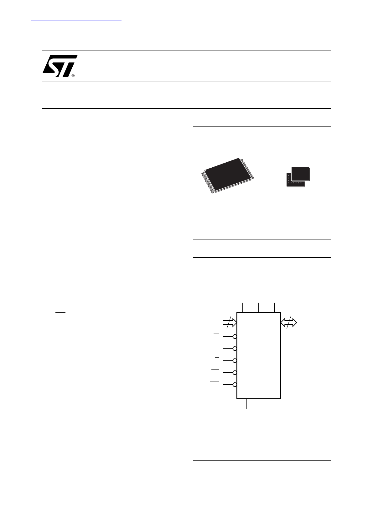
M28W16 0BT
M28W160BB
TSOP48 (N)
12 x 20mm
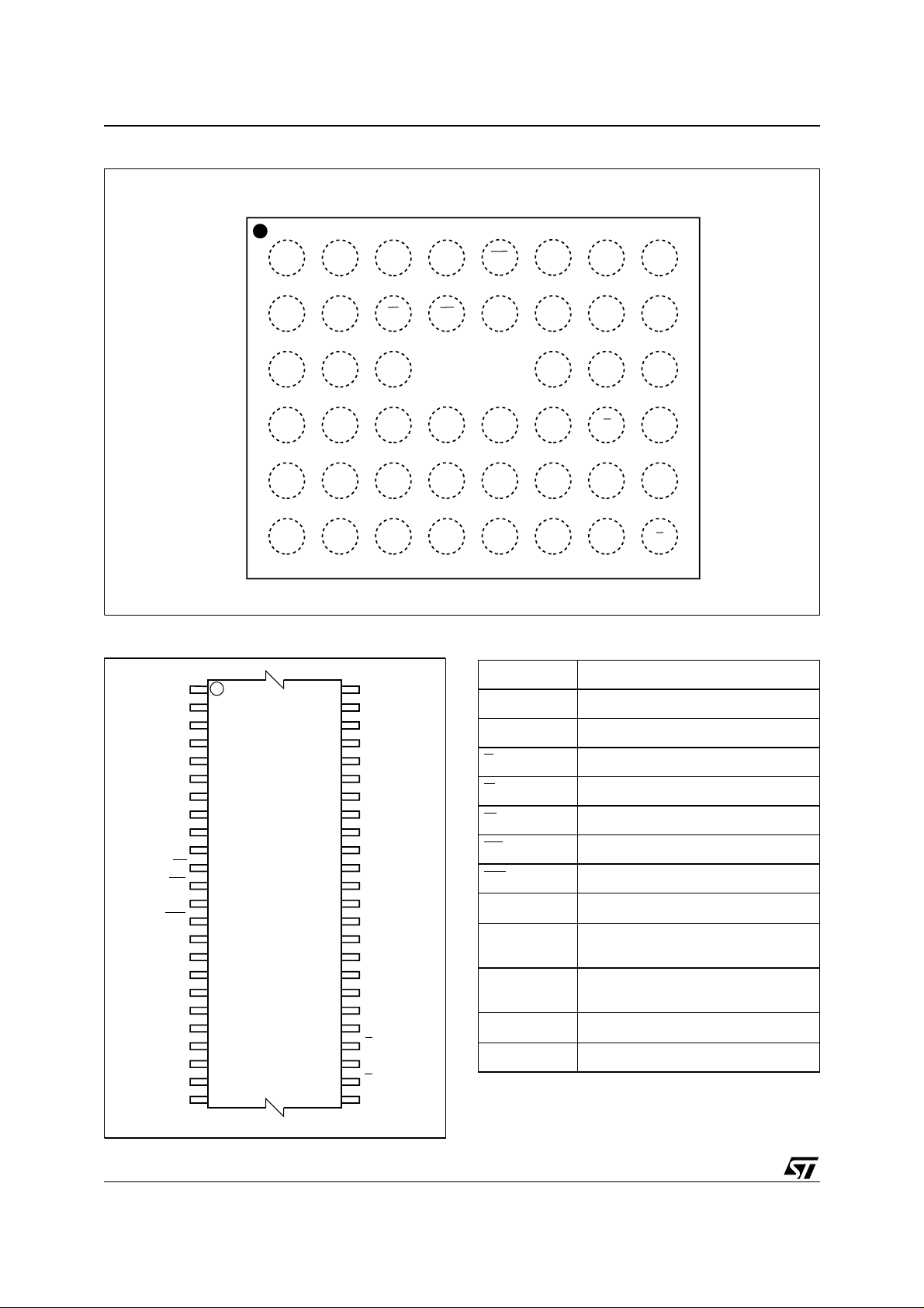
Figure 1. Logic Diagram
V
V
DDQVPP
DD
20
A0-A19
W
E
G
RP
WP
M28W160BT
M28W160BB
V
SS
µBGA
µBGA46 (GB)
8 x 6 solder balls
16
DQ0-DQ15
AI02628
1/39May 2000
M28W160BT, M28W160BB
Figure 2. µBG A Co nn e ct i ons (Top view through package)
87654321
A
B
C
D
E
F
V
DDQ
SS
Figure 3. TSOP Connection s
A15
A14
A13
A12
A11
A10 DQ14
V
WP
A19
A18
A17
1
A9
A8
NC
NC
W
RP
12
13
PP
A7
A6
A5
A4
A3
A2
24 25
A1
M28W160BT
M28W160BB
DQ15
48
37
36
AI02630
A8A11A13
DQ7V
DQ13
PP
RP A18
DQ11
DQ12
DQ4
WP A19
DQ2
DD
A7V
A5A17WA10A14
DQ0DQ9DQ3DQ6
DQ1DQ10V
A4
A2
A1A3A6A9A12A15
A0EDQ8DQ5DQ14A16
V
SS
G
AI02629
Table 1. Signal Names
A16
V
DDQ
V
SS
DQ15
DQ7
DQ6
DQ13
DQ5
DQ12
DQ4
V
DD
DQ11
DQ3
DQ10
DQ2
DQ9
DQ1
DQ8
DQ0
G
V
SS
E
A0
A0-A19 Address Inputs
DQ0-DQ7 Data Input/Output, Command Inputs
DQ8-DQ15 Data Input/Output
E
G
W
RP
WP
V
DD
V
DDQ
V
PP
V
SS
Chip Enable
Output Enable
Write Enable
Reset
Write Protect
Supply Voltage
Power Supply for
Input/Output Buffers
Optional Supply Voltage for
Fast Program & Erase
Ground
NC Not Connected Internally
2/39

M28W160BT, M28W160BB
Table 2. Absolute Maximum Ratings
Symbol Parameter Value Unit
T
A
T
BIAS
T
STG
V
IO
V
, V
DD
DDQ
V
PP
Note: 1. Except for the ratin g " Operating Temperature Range", stresses abo ve those listed in the T able "Abs ol ute Maximum Ratings" may
cause permanent damage to the device. These are stress ratings only and operation of the device at these or any other conditions
above those indi cated in the Operating sections of this s pecification is not impli ed. Exposure to Absolute M aximum Rating conditions for extended per iods may aff ect device reliabilit y. Refer also to the STMicroel ectronics SURE Program an d other relevan t qual ity docum en ts .
2. Depends on range.
Ambient Operating Temperature
Temperature Under Bias –40 to 125 °C
Storage Temperature –55 to 155 °C
Input or Output Voltage
Supply Voltage –0.6 to 4.1 V
Program Voltage –0.6 to 13 V
DESCRIPTION
The M28W160B is a 16 Mbit non-volatile Flash
memory that can be erased electrically at the block
level and programmed i n-system on a Word-byWord basis. The device is of fered in the TS OP48
(10 x 20mm) and the µ BGA46, 0.75 mm ball pitch
packages. When shipped, all bits of the
M28W160B are in the ‘1’ state.
The array matrix organisation allows each block to
be erased and reprogrammed without affecting
other blocks. Each block can be programmed and
erased over 100,000 cycles. V
DDQ
the I/O pin down t o 1.65V. An optional 12 V V
power supply is provided to speed up the program
phase at customer production line environment.
An internal Command Interface (C.I.) decodes the
instructions to access/modify the memory content.
The Program/Erase Controller (P /E.C.) automatically executes the algorithms taking care of the
timings necessary for program and erase operations. Verification is performed too, unburdening
the microcontroller, while the Status Register
tracks the status of th e operation.
The following instructions are executed by the
M28W160B: Read Array , Read Electronic Signature, Read Status Register, Clear Status Register,
Program, Double Word Program, Block Erase,
Program/Erase Suspend, Program/Erase Resume and CFI Query.
(1)
(2)
allows to driv e
PP
–40 to 85 °C
–0.6 to V
DDQ
+0.6
V
Organisation
The M28W160B is organised as 1 Mbit by 16 bits.
A0-A19 are the address l ines; DQ0 -DQ15 are the
Data Input/Output. Memory control is provided by
Chip Enable E
W
inputs. The Program and Erase operations are
, Output Enable G and Write Enable
managed automatically by the P/E.C. Block protection against Program or E rase provides additional data security.
The upper two (or lower two) parameter blocks
can be protected to secure the code content of the
memory . WP
controls protection and unprotection
operations.
Memory Blocks
The device features an asymmetrical blocked architecture. The M28W160B has an array of 39
blocks: 8 Parameter Blocks of 4 KWord and 31
Main Blocks of 32 KWord. M28W 160BT has the
Parameter Blocks at the top of the memory address space while the M28W160BB locates the
Parameter Blocks starting from the bottom. The
memory maps are shown in Tables 3 and 4.
The two upper parameter block c an be protected
from accidental programming or erasure using
. Each block can be erased separately. Erase
WP
can be suspended in order to perform either read
or program in any other b lock and then resum ed.
Program can be s uspended to read data in any
other block and then resumed.
3/39
M28W160BT, M28W160BB
Table 3. Top Boot Block Addresses,
M28W160BT
#
38 4 FF000-FFFFF
37 4 FE000-FEFFF
36 4 FD000-FDFFF
35 4 FC000-FCFFF
34 4 FB000-FBFFF
33 4 FA000-FAFFF
32 4 F9000-F9FFF
31 4 F8000-F8FFF
30 32 F0000-F7FFF
29 32 E8000-EFFFF
28 32 E0000-E7FFF
27 32 D8000-DFFFF
26 32 D0000-D7FFF
25 32 C8000-CFFFF
24 32 C0000-C7FFF
23 32 B8000-BFFFF
22 32 B0000-B7FFF
21 32 A8000-AFFFF
20 32 A0000-A7FFF
19 32 98000-9FFFF
18 32 90000-97FFF
17 32 88000-8FFFF
16 32 80000-87FFF
15 32 78000-7FFFF
14 32 70000-77FFF
13 32 68000-6FFFF
12 32 60000-67FFF
11 32 58000-5FFFF
10 32 50000-57FFF
9 32 48000-4FFFF
8 32 40000-47FFF
7 32 38000-3FFFF
6 32 30000-37FFF
5 32 28000-2FFFF
4 32 20000-27FFF
3 32 18000-1FFFF
2 32 10000-17FFF
1 32 08000-0FFFF
0 32 00000-07FFF
Size
(KWord)
Address Range
Table 4. Bottom Boot Block Addresses,
M28W160BB
#
38 32 F8000-FFFFF
37 32 F0000-F7FFF
36 32 E8000-EFFFF
35 32 E0000-E7FFF
34 32 D8000-DFFFF
33 32 D0000-D7FFF
32 32 C8000-CFFFF
31 32 C0000-C7FFF
30 32 B8000-BFFFF
29 32 B0000-B7FFF
28 32 A8000-AFFFF
27 32 A0000-A7FFF
26 32 98000-9FFFF
25 32 90000-97FFF
24 32 88000-8FFFF
23 32 80000-87FFF
22 32 78000-7FFFF
21 32 70000-77FFF
20 32 68000-6FFFF
19 32 60000-67FFF
18 32 58000-5FFFF
17 32 50000-57FFF
16 32 48000-4FFFF
15 32 40000-47FFF
14 32 38000-3FFFF
13 32 30000-37FFF
12 32 28000-2FFFF
11 32 20000-27FFF
10 32 18000-1FFFF
9 32 10000-17FFF
8 32 08000-0FFFF
7 4 07000-07FFF
6 4 06000-06FFF
5 4 05000-05FFF
4 4 04000-04FFF
3 4 03000-03FFF
2 4 02000-02FFF
1 4 01000-01FFF
0 4 00000-00FFF
Size
(KWord)
Address Range
4/39

M28W160BT, M28W160BB
SIGNAL DESCRIPTIONS
See Figure 1 and Table 1.
Address Inputs (A0-A19). The address signals
are inputs driven with CMOS vol tage level s. They
are latched during a write operation.
Data Input/Output (DQ0-DQ15). The data inputs, a word to be programmed or a comm and to
the C.I., are latched on the Chip Enable E
Enable W
rising edge, whichever occurs first. The
or Write
data output from the memory Array, the Electronic
Signature or Status Register is valid when Chip
Enable E
and Output Enable G are active. The
output is high impedance when the ch ip is deselected, the outputs are disabled or RP
is tied to VIL.
Commands are issued on DQ0-DQ7.
Chip Enable (E
). The Chip Enable input acti-
vates the memory control logic, input buffers, decoders and sense amplifiers. E
at VIH deselects
the memory and red uces the power consumption
to the stand-by level. E
can also be used to control
writing to the command register and to the memory array, while W
Output Enable (G
remains at VIL.
). The Output Enable controls
the data Input/Output buffers.
Write Enable (W
). This input controls writing to
the Command Register, Input Address and Dat a
latches.
Write Protect (WP
). Write Protect is an input to
protect or unprotect the two lockable parameter
blocks. When WP
is at VIL, the locka ble bl ocks are
protected. Program or erase operations are not
achievable. When WP
is at VIH, the lockable
blocks are unprotected and they can be programmed or erased (refer to Table 9).
Reset Input (RP
ware reset of the memory. When RP
). The RP input provides hard-
is at VIL, the
memory is in reset mode : the outputs are put to
High-Z and the current consumption is minimised.
When RP
is at VIH, the device is in norm al operation. Exiting reset mode the device enters read array mode.
V
Supply Voltage (2.7V to 3.6V). VDD pro-
DD
vides the power supply to the internal core of the
memory device. It is the main power supply for all
operations (Read, Program and Erase). It ranges
from 2.7V to 3.6V.
Supply Voltage (1.65V to VDD). V
V
DDQ
DDQ
provides the power supply to the I/O pins and enables all Outputs to be powered independently
from V
DD
. V
can be tied to VDD or it can use a
DDQ
separate supply. It can be powered either from
1.65V to 2.2V or from 2.7V to 3.6V.
Program Supply Voltage (12V). VPP is
V
PP
both a control input and a power supply pin. T he
two functions are selected by the voltage range
applied to the pin.
is kept in a low voltage range (0V to 3.6V)
If V
PP
V
is seen as a control input. In this case a volt-
PP
age lower than V
against program or erase, whi le V
ables these functions. V
gives an absolute protection
PPLK
value is only sampled
PP
PP
> V
PP1
en-
at the beginning of a program or erase; a cha nge
in its value after the operation has been started
does not have any effect and program or erase are
carried on regu larl y.
is used in the range 11.4V to 12.6V acts as
If V
PP
a power supply pin. In this condition V
PP
value
must be stable until P/E algorithm is completed
(see Table 22 and 23).
Ground. VSS is the reference for all the volt-
V
SS
age measurements.
5/39
M28W160BT, M28W160BB
DEVICE OPERATIONS
Four control pins rule the hardware access t o the
Flash memory: E
, G, W, RP. The following operations can be performed using the appropriate bus
cycles: Read, Write the Command of an Instruction, Output Disable, Stand-by, Reset (see Table
5).
Read. Read operations are used to output the
contents of the Memory Array, the Electronic Signature, the Status Register and the CFI. Both Chip
Enable (E
) and Output Enabl e (G) must be at V
in order to perform the read operation. The Chip
Enable input should be used to enable the device.
Output Enable shoul d be used to gate data onto
the output indepe ndently of the device s election.
The data read depend on the previous command
written to the memory (see instructions RD, RSIG,
RSR, RCFI). Read Array is the default state of the
device when exiting Reset or after power-up.
Write. Write operations are used to give Commands to the memory or to latch Input Data to be
programmed. A write operation is initiated when
Chip Enable E
Output Enable G
Table 5. User Bus Operations
Operation E G W RP WP
Read
Write
Output Disable
Stand-by
Reset X X X
Note: 1. X = VIL or VIH, V
and Write Enable W are at VIL with
at VIH. Comm ands, Inp ut Data
(1)
V
IL
V
IL
V
IL
V
IH
= 12V ± 5%.
PPH
V
IL
V
IH
V
IH
XX
V
IH
V
IL
V
IH
and Addresses are latched on the rising edge of W
or E, whichever occur first.
Output Disa bl e . The data outputs are high impedance when the Output Enable G
Stand-by. Stand-by disables most of the internal
circuitry allowing a substantial reduction of the current consumption. The memory is in stand-by
when Chip Enable E
read mode. The power consumption is reduced to
the stand-by level and the o utputs are set to high
impedance, independently from the Output Enable
IL
G
or Write Enable W inputs. If E switches to V
during program or erase operation, the device enters in stand-by when finished.
Reset. During Reset mode all internal circuits are
switched off, the memory is deselected and the
outputs are put in high impedance. The memory is
in Reset mode when RP
sumption is reduced to the Stand-by level, independently from the Chip Enabl e E
or Write Enable W inputs. If RP is pulled to V
G
during a Program or Erase, this operation is aborted and the memory content is no longer valid as it
has been compromised by the aborted operation.
V
IH
V
IH
V
IH
V
IH
V
IL
is at VIH.
is at VIH and the device is in
is at VIL. The power con-
, Output En able
V
PP
X Don’t Care Data Output
V
X
X Don’t Care Hi-Z
X Don’t Care Hi-Z
X Don’t Care Hi-Z
DD
or V
PPH
DQ0-DQ15
Data Input
IH
SS
Table 6. Read Electronic Signature (RSIG Instruction)
Code Device E
Manufact. Code
M28W160BT
Device Code
M28W160BB
Note: 1. RP = VIH.
6/39
V
IL
V
IL
V
IL
G W A0 A1-A7 A8-A19 DQ0-DQ7 DQ8-DQ15
V
V
V
V
IL
IL
IL
IH
V
IH
V
IH
V
V
V
V
IL
IH
IH
Don’t Care 20h 00h
IL
V
Don’t Care 90h 00h
IL
V
Don’t Care 91h 00h
IL

M28W160BT, M28W160BB
INSTRUCTIONS AND COMMANDS
Eleven instructions are available (see Tables 7
and 8) to perform Read Memory Array, Read Status Register, Read Electronic Signature, CFI Query, Erase, Program, Dou ble Word Program, Clear
Status Register, Program/Erase Suspend and
Program/Erase Resume. Status Register output
may be read at any time, during programming or
erase, to monitor the progress of the operation.
An internal Command Interface (C.I.) decodes the
instructions while an internal Program/Erase Controller (P/E.C.) handles all timing and verifies the
correct execution of the Program and Erase instructions. P/E.C. provides a Status Register
whose bits indicate operation and exit status of the
internal algorithms.
The Command Interface is reset to Read Array
when power is first applied, when exiting from Reset or whenever V
is lower than V
DD
LKO
. Command sequence must be followed exactly. Any
invalid combination of commands will reset the device to Read Array.
Read (RD)
The Read instruction consists of one write cycle
(refer to Device Operations section) giving the
command FFh. Next read operations will read the
addressed location and output the data. When a
device reset occurs, the memo ry is in Read Array
as default.
Read Status Register (RSR)
The Status Register indicates when a program or
erase operation is complete and the success or
failure of operation itself. Issue a Read Status
Register Instruction (70h) to rea d the S tatu s Register content.
The Read Status Register instruction may be issued at any time, also when a Program/Erase operation is ongoing. The following Read operations
output the content of the Status Register. The Status Register is latched on the falling edge of E
G
signals, and can be read until E or G returns to
V
. Eithe r E or G must be t oggled to updat e the
IH
or
latched data. Additionally, any read attempt during
program or erase operation will autom atically ou tput the content of the Status Register.
Read Electronic Signature (RSIG)
The Read Electronic Signature instruction consists of one write cycle (refer to Device Operations
section) giving the command 90h. A subsequent
read will output the Manufacturer or the Device
Code (Electronic Signature) depending on the levels of A0 (see Tables 6). The Electronic Signature
can be read from the memory allowing programming equipment or applications to automatically
match their interface to the characteristics of
M28W160B. The Manufacturer Code is output
when the address lines A 0 is at V
Code is output when A0 is at V
must be kept to V
, other addresses are ignored.
IL
, the Device
IL
. Address A1-A7
IH
The codes are output on DQ0-DQ7 with DQ8DQ15 at 00h.
CFI Query (RCFI)
The Common Flash Interface Query mode is entered by writing 98h. Next read operations will read
the CFI data. The CFI data structure contains also
a security area; in this section, a 64 bit unique security number is written, starting at address 80h.
This area can be accessed only in read mode by
the final use and there are no ways of chang ing
the code after it has been written by ST. Write a
read instruction to return to Read mode (refer to
the Common Flash Interface section).
Table 7. Commands
Hex Code Command
00h, 01h, 60h,
2Fh, C0h
10h Alternative Program Set-up
20h Erase Set-up
30h Double Word Program Set-up
40h Program Set-up
50h Clear Status Register
70h Read Status Register
90h or 98h
B0h Program/Erase Suspend
D0h
FFh Read Array
Invalid/Reserved
Read Electronic Signature, or
CFI Query
Program/Erase Resume, or
Erase Confirm
7/39

M28W160BT, M28W160BB
Table 8. Instructions
Mne-
monic
RD
RSR
RSIG
RCFI CFI Qu ery 1+ Wri te 55h
EE Erase 2 Write X 20h Write
PG Progra m 2 Write X
DPG
CLRS
PES
PER
Note: 1. X = Don’t Care.
Instruction Cycles
Read Memory
Array
Read Status
Register
Read
Electronic
Signature
Double Word
(4)
Program
Clear Status
Register
Program/
Erase
Suspend
Program/
Erase
Resume
2. The first cyc le of the RD, RSR, RSIG o r RCFI in st ruction is followed by read oper ations to read me m ory array, Status Register or
Electronic Signature codes. Any number of Read cycle can occur after one command cycle.
3. Signature address bit A0=V
kept to V
4. Address 1 and Address 2 must be consecuti ve Addresses differing only for address bit A0.
. Other address bits are i gnored.
IL
Operat.
1+ Write X FFh
1+ Write X 70h
1+ Write X
3 Write X 30h Write Address 1
1Write X 50h
1Write X B0h
1Write X D0h
IL
1st Cycle 2nd Cy cle 3nd Cy cle
(1)
Addr.
will output Manufacturer code. Address bit A0=V
Data Operat. Addr. Data Operat. Addr. Data
Read
90h or
98h
98h or
90h
40h or
10h
(2)
Read
Read
Read
Read
Write Address
(2)
(2)
(2)
Address
Signature
Address
CFI
Address
Bloc k
Address
X
IH
Data
Status
Register
Signatur e
(3)
Query
D0h
Data
Input
Data
Input
will output Device code. Address A7-A1 must be
Write Address 2
Data
Input
Erase (EE)
Block erasure sets all the bits within the selected
block to ’1’. One block at a time can be erased. It
is not necessary to program the block with 00h as
the P/E.C. will do it automatically before erasing.
This instruction uses two write cycles. The first
command written is the Erase Set up command
20h. The second command is the Erase Confirm
command D0h. An address within the block to be
erased is given and latched in to the mem ory during the input of t he second com mand. If the s econd command given is not an erase conf irm, the
status register bits b4 and b5 are set and the instruction aborts.
Read operations output the status register after
erasure has started.
8/39
Status Register bit b7 returns ’0’ while the erasure
is in progress and ’1’ when it has completed. After
completion the Status Register bit b5 returns ’1’ if
there has been a n Erase Failure. S tatus register
bit b1 returns ’1’ if the user is attempt ing to program a protected blo ck. S tat us Regi s ter bit b3 returns a ’1’ if V
is below V
PP
Erase aborts if RP
turns to VIL. As da ta integ rity
PPLK
.
cannot be guaranteed when the erase operation is
aborted, the erase must be repeated. A Clear Status Register instruction must be issued to reset b1,
b3, b4 and b5 of th e Status Register. During the
execution of the erase by t he P /E.C., the memory
accepts only the RSR (Read Status Register) and
PES (Program/Erase Suspend) instructions.
Table 9. Memory Blocks Protection Truth Table
VPP
(1,3)
RP
(2,4)
WP
(1,4)
M28W160BT, M28W160BB
Lockable Blocks Other Blocks
X
V
IL
V
or V
DD
V
or V
DD
Note: 1. Notes:1. X ’ = Don’t Care
2. RP
3. V
4. V
5. V
(5)
PPH
(5)
PPH
is the Reset/Power Down.
is the program or erase supply volta ge.
PP
are logic high and low levels.
IH/VIL
must be also gr eater than the Program V ol t age Lock-Out V
PP
V
IL
V
IH
V
IH
V
IH
Table 10. Status Register Bits
Mnemonic Bit Name
P/ECS 7 P/E.C. Status
Erase
ESS 6
ES 5 Erase Status
PS 4
VPPS 3
PSS 2
BPS 1
Suspend
Status
Program
Status
Status
V
PP
Program
Suspend
Status
Block
Protection
Status
X Protected Protected
X Protected Protected
Logic
Level
V
IL
V
IH
Definition Note
Protected Unprotected
Unprotected Unprotected
.
PPLK
’1’ Ready Indicates the P/E.C. status, check during
Program or Erase, and on completion before
’0’ Busy
’1’ Suspended
In progress or
’0’
Completed
checking bits b4 or b5 for Program or Erase
Success
On an Erase Suspend instruction P/ECS and
ESS bits are set to ’1’. ESS bit remains ’1’ until an
Erase Resume instruction is given.
’1’ Erase Error ES bit is set to ’1’ if P/E.C. has applied the
maximum number of erase pulses to the block
’0’ Erase Success
’1’ Program Error
’0’ Program Success
V
’1’
Invalid, Abort VPPS bit is set if the VPP voltage is below V
PP
without achieving an erase verify.
PS bit set to ’1’ if the P/E.C. has failed to program
a word.
when a Program or Erase instruction is executed.
is sampled only at the beginning of the
V
V
’0’
PP
OK
’1’ Suspended
In Progress or
’0’
Completed
PP
Erase/Program operation.
On a Program Suspend instruction P/ECS and
PSS bits are set to ’1’. PSS remains ’1’ until a
Program Resume Instruction is given
Program/Erase on
’1’
protected Block,
Abort
No operation to
’0’
protected blocks
BPS bit is set to ’1’ if a Program or Erase
operation has been attempted on a protected
block
PPLK
0 Reserved
Note: Logic level ’1’ is High, ’0’ is Low.
9/39

M28W160BT, M28W160BB
Program (PG)
The memory array can be programmed word-byword. This instruction uses two write cycles. The
first command written is the Program Set-up command 40h (or 10h). A second write operation latches the Address and the Data to be written and
starts the P/E.C.
Read operations output the Status Register content after the programming has started. The Status
Register bit b7 returns ’0’ while t he programming
is in progress and ’1’ when it has completed. After
completion the Status register bit b4 returns ’1’ if
there has been a Program Failure. Status register
bit b1 returns ’1’ if the user is attempt ing to program a protected blo ck. S tatu s Regi s ter bit b3 returns a ’1’ if V
aborts if RP
is below V
PP
. Programming
PPLK
goes to VIL. As data integrity cannot
be guaranteed when the program operation is
aborted, the memory location must be erased and
reprogrammed. A Clear Status Register instruction must be issued to reset b4, b3 and b1 of the
Status Register.
During the execution of the program by the P/E.C.,
the memory accepts only the RSR (Read Status
Register) and PES (Program/Erase Suspe nd) instructions.
Doubl e Word Prog ram (DPG)
This feature is offered to improve the programming
throughput, writing a page of two adjacent words
in parallel.The two words m ust differ only for the
address A0. Programm ing should not b e att emp ted when V
is not at V
PP
also be executed if V
PP
. The operation can
PPH
is below V
PPH
but result
could be uncertain. This instruction uses three
write cycles. The first c ommand written is the Double Word Program Set-Up command 30h. A second write operation latc hes the Address and the
Data of the first w ord to be wri tten, the third write
operation latches the Address and the Data of the
second word to be written and starts the P/E.C.
Read operations output the Status Register content after the programming has started. The Status
Register bit b7 returns ’0’ while t he programming
is in progress and ’1’ when it has completed. After
completion the Status register bit b4 returns ’1’ if
there has been a Program Failure. Status register
bit b1 returns ’1’ if the user is attempt ing to program a protected blo ck. S tatu s Regi s ter bit b3 returns a ’1’ if V
aborts if RP
goes to VIL. As data integrity cannot
is below V
PP
. Programming
PPLK
be guaranteed when the program operation is
aborted, the memory location must be erased and
reprogrammed. A Clear Status Register instruction must be issued to reset b4, b3 and b1 of the
Status Register.
During the execution of the program by the P/E.C.,
the memory accepts only the RSR (Read Status
Register) and PES (Program/Erase Suspe nd) instructions.
Clear Status Register (CLRS)
The Clear Status Register uses a single write operation which clears bits b1, b3, b4 and b5 to ‘0’.
Its use is necessary before any new operation
when an error has been detected.
The Clear Status Register is executed w riting the
command 50h.
Program/Erase Suspend (PES)
Program/Erase suspend is accepted only during
the Program Erase instruction execu tion. When a
Program/Erase Suspend command is written to
the C.I., the P/E.C. freezes the Program/Erase operation. Program/Erase Res ume (P ER) cont inues
the Program/Erase operation. Program/Erase
Suspend consists of writing the command B0h
without any specific address.
The Status Register bit b2 is set to ‘1’ (within 5µs)
when the program has been sus pended . b2 is set
to ‘0’ in case the program is completed or in
progress. The Status Register bit b6 is set to ‘1’
(within 30µs) when the erase has been sus pended. b6 is s et t o ‘0’ in cas e th e e rase is com plet ed
or in progress. The valid commands while erase is
suspended are Program/Erase Resume, Program, Read Array, Read Status Register, Read
Identifier, CFI Query. While program is suspended
the same command set is valid except for program
instruction. During program/erase suspend mode,
the chip can be placed in a pseudo-stand-by mode
by taking E
sumption. Program/Erase is aborted if RP
.
V
IL
to VIH. This reduces active current con-
turns to
Program/Erase Resume (PER)
If a Program/Erase Suspend instruction was previously executed, the program/erase operation may
be resumed by issuing the command D0h. The
status register bit b2/b6 is cleared when program/
erase resumes. Read operations output the status
register after the program/erase is resumed.
The suggested flow charts for programs that use
the programming, erasure and program/erase
suspend/resume features of the memories are
shown from Figures 10, 11, 12, 13 and 14.
10/39
M28W160BT, M28W160BB
Table 11. Program, Erase Times and Program /Eras e Endur ance Cycles
(T
= 0 to 70°C or –40 to 85°C; VDD = 2.7V to 3.6V)
A
Parameter Test Conditions
V
Word Program
Double Word Program
Main Block Program
Parameter Block Program
Main Block Erase
Parameter Block Erase
PP
V
= 12V ±5%
PP
V
= 12V ±5%
PP
V
PP
V
= 12V ±5%
PP
V
PP
V
= 12V ±5%
PP
V
PP
= 12V ±5%
V
PP
V
PP
= V
= V
= V
= V
= V
DD
DD
DD
DD
DD
Program/Erase Cycles (per Block) 100,000 cycles
Note: TA = 25 °C.
Min
M28W160B
Typ
(1)
Max
Unit
10 200 µs
10 200 µs
0.16 5 sec
0.32 5 sec
0.02 4 sec
0.04 4 sec
110 sec
110 sec
0.8 10 sec
0.8 10 sec
11/39

M28W160BT, M28W160BB
BLOCK PROTECTION
Two parameter blocks (#0 and #1) can be protected against Program or Erase to ensure extra data
security. Unprotected blocks can be programmed
or erased.
tied to VIL protects the two lockable b locks.
WP
V
below V
PP
protects all the blo cks. A ny pro-
PPLK
gram or erase operation on protected blocks is
aborted. The Status Register tracks when the
event occurs.
Table 9 defines the protection methods.
POWER CONSUMPTION
The M28W160B puts itself in one o f four different
modes depending on the statu s of the c ontrol signals: Active Power, Automatic Stand-by, Stand-by
and Reset define decreasing levels of current consumption. These allow the memory power to be
minimised, in turn decreasing the overall system
power consumption. As different recovery time are
linked to the different modes, please refer to the
AC timing table to design your system.
Active Power
When E
is at VIL and RP is at VIH, the device is in
active mode. Refer to DC Characteristics to get
the values of the current supply consumption.
Automatic Stand-by
Automatic Stand-by provides a low power consumption state during read mode. Following a
read operation, after a del ay c lose to the memory
access time, the device enters Automatic Standby: the Supply Current is reduced to I
CC1
values.
The device keeps the last output data s table, till a
new location is accessed.
Stand-by or Reset
Refer to the Device Operations section.
Power Up
The Supply voltage V
voltage V
can be applied in any order. The
PP
and the Program S upply
DD
memory Command Interface is reset on power up
to Read Memory Array, but a negative transition of
Chip Enable E
or a change of the addresses is required to ensure valid data outputs. Care must be
taken to avoid w rites to t he memory when V
above V
ther E
. Writes can be inhibited by drivin g ei-
LKO
or W to VIH. The memory is disabled if RP
DD
is
is at VIL.
Supply Rails
Normal precautions must be taken for supply voltage decoupling, each device in a system should
have the V
0.1µF capacitor close to the V
and VPP rails decoupled with a
DD
and VPP pins.
DD
The PCB trace widths should be sufficient to carry
the required V
program and erase currents.
PP
12/39
 Loading...