

■ Fast Access Time:
–90nsatVCC=5 V forM28C64 andM28C64-A
– 120 ns at VCC=3 V for M28C64-xxW
■ Single Supply Voltage:
– 4.5 V to 5.5V for M28C64 and M28C64-A
– 2.7 V to 3.6V for M28C64-xxW
■ Low Power Consumption
■ Fast BYTE and PAGE WRITE (up to 64 Bytes)
– 1 ms at VCC=4.5 V for M28C64-A
– 3 ms at VCC=4.5 V for M28C64
– 5 ms at VCC=2.7 V for M28C64-xxW
■ Enhanced Write Detection and Monitoring:
– Ready/Busy Open DrainOutput
– Data Polling
– Toggle Bit
– Page Load Timer Status
■ JEDEC Approved Bytewide Pin-Out
■ Software Data Protection
■ 100000 Erase/Write Cycles (minimum)
■ Data Retention (minimum):
– 40 Years for M28C64 and M28C64-xxW
– 10 Years for M28C64-A
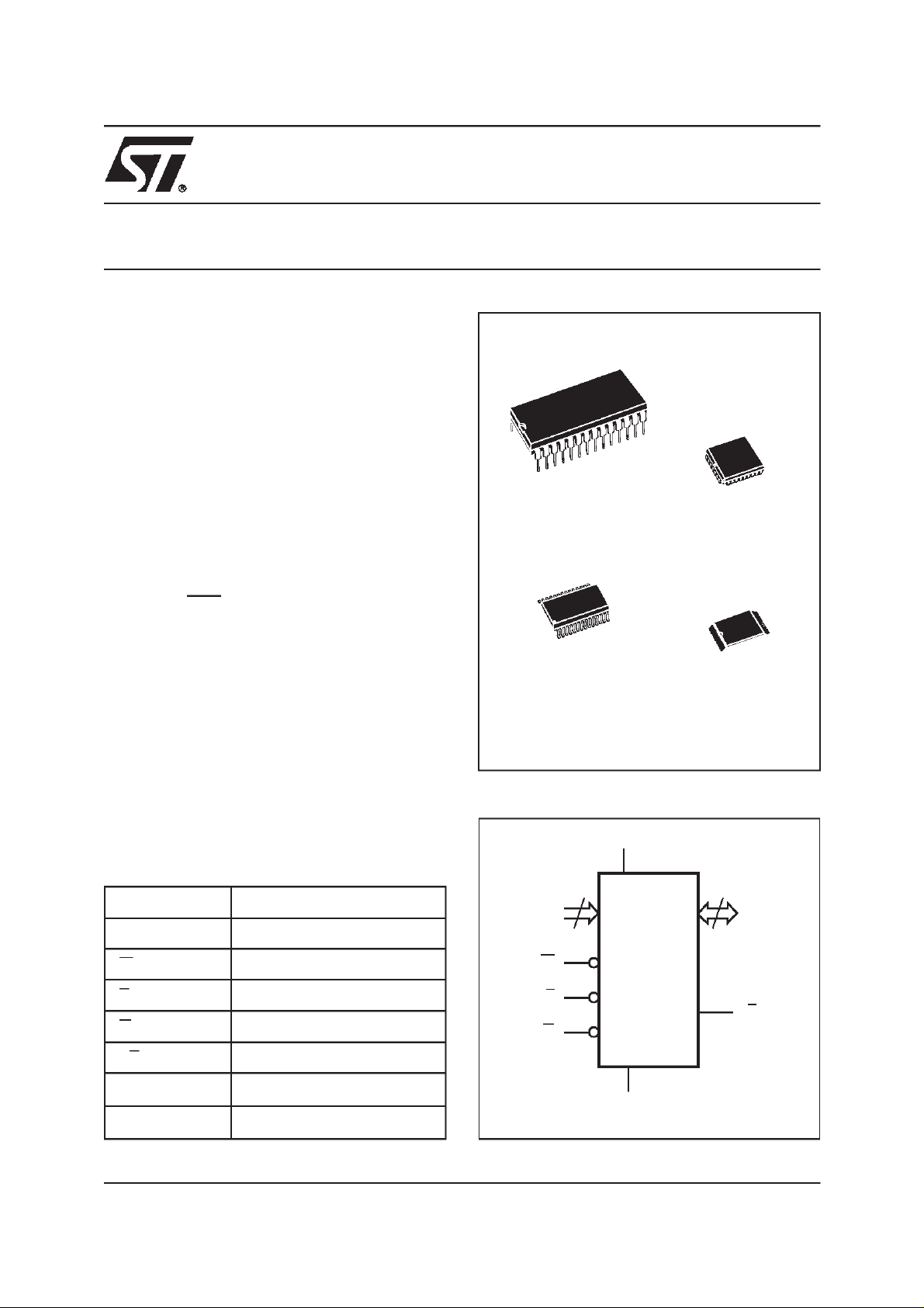
M28C64
64 Kbit (8K x 8) Parallel EEPROM
With Software Data Protection
28
1
PDIP28 (BS)
28
1
SO28 (MS)
300 mil width
Figure 1. Logic Diagram
V
CC
PLCC32 (KA)
TSOP28 (NS)
8 x 13.4 mm
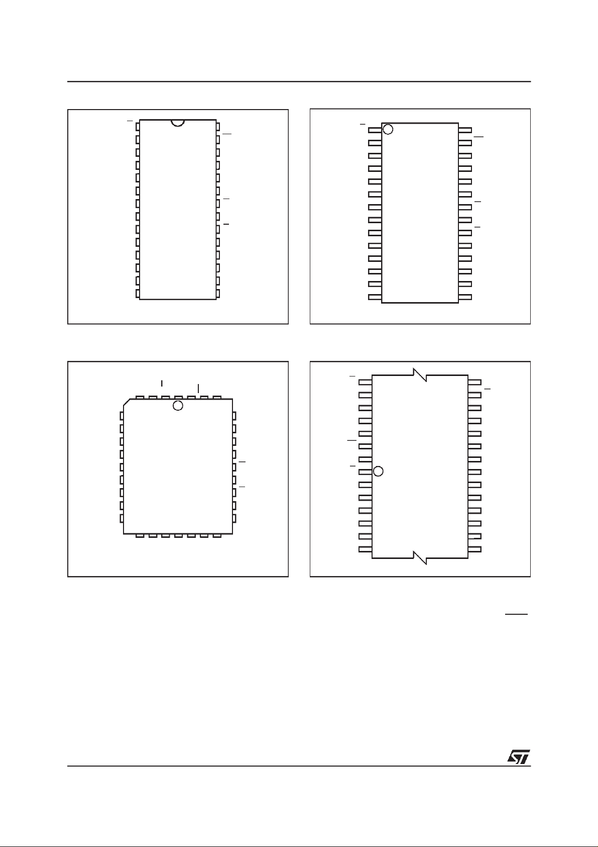
Table 1. Signal Names
A0-A12 Address Input
DQ0-DQ7 Data Input / Output
W Write Enable
E Chip Enable
G Output Enable
RB Ready / Busy
V
CC
V
SS
Supply Voltage
Ground
A0-A12
W
13
M28C64
E
G
V
SS
8
DQ0-DQ7
RB
AI01350C
1/24June 2000
M28C64
Figure 2A. DIP Connections
RB V
1
A12
2
A7
3
A6
4
A5
5
A4
6
A3
7
8
9
10
11
12
13
14
M28C64
AI01351C
A2
A1
A0
DQ0
DQ2
SS
Note: 1. NC = Not Connected
Figure 2B. PLLC Connections
CC
RB
A7
A6
A5
A4
A3
A2
9
A1
A0
NC
DQ0
DQ1
Note: 1. NC = Not Connected
2. DU = Do Not Use
A12
1
M28C64
17
SS
V
DQ2
DU
32
DU
V
DQ3
28
27
26
25
24
23
22
21
20
19
18
17
16
15
W
DQ4
CC
W
NC
A8
A9
A11
G
A10
E
DQ7
DQ6
DQ5DQ1
DQ4
DQ3V
NC
25
DQ5
A8
A9
A11
NC
G
A10
E
DQ7
DQ6
AI01352D
Figure 2C. SO Connections
RB
A12
DQ0
DQ1
DQ2
V
SS
Note: 1. NC =Not Connected
A7
A6
A5
A4
A3
A2
A1
A0
1
2
3
4
5
6
7
8
9
10
11
12
13
14
M28C64
AI01353C
Figure 2D. TSOP Connections
G
22
A11
A9
A8
NC
W
V
CC
RB
A12
Note: 1. NC =Not Connected
28
M28C64
1
A7
A6
A5
A4
A3
78
AI01354C
V
28
27
26
25
24
23 A11
22
21
20
19
18
17
16
15
CC
W
NC
A8
A9
G
A10
E
DQ7
DQ6
DQ5
DQ4
DQ3
21
15
14
A10
E
DQ7
DQ6
DQ5
DQ4
DQ3
V
SS
DQ2
DQ1
DQ0
A0
A1
A2
DESCRIPTION
The M28C64 devices consist of 8192x8 bits of low
power, parallel EEPROM, fabricated with
STMicroelectronics’ proprietary single polysilicon
CMOS technology. The devices offer fast access
time, with low power dissipation, and require a
single voltage supply (5V or 3V, depending on the
option chosen).
The device has been designed to offer a flexible
microcontroller interface, featuring both hardware
2/24
and software handshaking, with Ready/Busy,
Data Polling and Toggle Bit. The device supports
a 64 byte Page Write operation. Software Data
Protection (SDP) is also supported, using the
standard JEDEC algorithm.
M28C64
Table 2. Absolute Maximum Ratings
1
Symbol Parameter Value Unit
T
A
T
STG
V
CC
V
IO
V
I
V
ESD Electrostatic Discharge Voltage (Human Body model)
Note: 1. Except for the rating “Operating Temperature Range”, stresses above those listed in the Table “Absolute Maximum Ratings” may
cause permanent damage to the device. These arestress ratings only, and operation of the device at these or any other conditions
above those indicated in the Operating sections of this specification is not implied. Exposure to Absolute Maximum Rating conditions for extended periods may affect device reliability. Refer also to the ST SURE Program and other relevant quality documents.
2. MIL-STD-883C, 3015.7 (100 pF, 1500 Ω)
Ambient Operating Temperature -40 to 125 °C
Storage Temperature -65 to 150 °C
Supply Voltage -0.3 to VCC+1 V
Input or Output Voltage
-0.6 to V
CC
+0.6
V
Input Voltage -0.3 to 6.5 V
2
4000 V
Figure 3. Block Diagram
RB E G W
A6-A12
(Page Address)
A0-A5
VPPGEN RESET
ADDRESS
LATCH
ADDRESS
LATCH
Y DECODE
X DECODE
CONTROL LOGIC
64K ARRAY
SENSE AND DATA LATCH
I/O BUFFERS
DQ0-DQ7
PAGE
LOAD
TIMER STATUS
TOGGLE BIT
DATA POLLING
AI01355
3/24
M28C64
IH
or V
1
; V=12V ± 5%.
IL
Ready/Busy (RB). Ready/Busy is an open drain
output that can be used to detect the end of the
internal write cycle.
DEVICE OPERATION
In order to prevent datacorruption and inadvertent
write operations, an internal VCCcomparator
inhibits the Write operations if the VCCvoltage is
lowerthan VWI(see Table 4A and Table4B). Once
the voltage applied on the VCCpin goes over the
VWIthreshold (VCC>VWI), write access to the
memory is allowed after a time-out t
specified in Table 4A and Table 4B.
Further protection against data corruption is
offered by the E and W low pass filters: any glitch,
on the E and W inputs, witha pulsewidth less than
10 ns (typical) is internally filtered out to prevent
inadvertent write operations to the memory.
Table 3. Operating Modes
Mode E G W DQ0-DQ7
Stand-by 1 X X Hi-Z
Output Disable X 1 X Hi-Z
Write Disable X X 1 Hi-Z
Read 0 0 1 Data Out
Write 0 1 0 Data In
Chip Erase 0 V 0 Hi-Z
Note: 1. 0=VIL;1=VIH;X=V
SIGNAL DESCRIPTION
The external connections to the device are
summarized in Table 1,and their use in Table 3.
Addresses (A0-A12). The address inputs are
used to select one byte from the memory array
during a read or write operation.
Data In/Out (DQ0-DQ7). The contents of the data
byte arewritten to,or read from,the memory array
through the Data I/O pins.
Chip Enable (E). The chip enable input must be
held low to enable read and write operations.
When Chip Enable is high, power consumption is
reduced.
Output Enable (G). The Output Enable input
controls the data output buffers, and is used to
initiate read operations.
Write Enable(W). TheWrite Enable input controls
whether the addressed locationis to be read, from
or written to.
PUW
,as
Table 4A. Power-Up Timing1for M28C64 (5V range)
(TA= 0 to70 °C or –40 to 85 °C or –40 to 125 °C; VCC= 4.5 to 5.5 V)
Symbol Parameter Min. Max. Unit
t
PUR
t
PUW
V
WI
Note: 1. Sampled only, not 100% tested.
Time Delay to Read Operation 1 µs
Time Delay to Write Operation (once VCC≥ VWI)10ms
Write Inhibit Threshold 3.0 4.2 V
Table 4B. Power-Up Timing1for M28C64-xxW (3V range)
(TA= 0 to70 °C or –40 to 85 °C; VCC= 2.7 to 3.6 V)
Symbol Parameter Min. Max. Unit
t
PUR
t
PUW
V
WI
Note: 1. Sampled only, not 100% tested.
4/24
Time Delay to Read Operation 1 µs
Time Delay to Write Operation (once VCC≥ VWI)15ms
Write Inhibit Threshold 1.5 2.5 V
M28C64
Read
The deviceis accessed like a static RAM. When E
and G are low, and W is high, the contents of the
addressed location are presented on the I/O pins.
Otherwise, when either G or Eis high,the I/Opins
revert to their high impedance state.
Write
Write operations are initiated when both W and E
are low and G is high. The device supports both
W-controlled and E-controlled write cycles (as
shown in Figure 11 and Figure12). The address is
latched during the falling edge of W or E (which
ever occurs later) and the data is latched on the
rising edge of W or E (which ever occurs first).
After a delay, t
, that cannot be shorter than
WLQ5H
the value specified in Table 10Ato Table 10C, the
internal write cycle starts. It continues, under
internal timing control, until the write operation is
complete. The commencement of this period can
be detected by reading the Page Load Timer
Status on DQ5. The end of the cycle can be
detected by reading the status of the Data Polling
and the Toggle Bit functions on DQ7 and DQ6.
Page Write
The Page Write mode allows up to 64 bytes to be
written on a single page in a single go. This is
achieved through a series of successive Write
operations, notwoof which are separatedbymore
than the t
WLQ5H
value (as specified in Table 10A
to Table 10C).
All bytes must be located on the same page
address (A12-A6 must be the same for all bytes).
The internal write cycle can start at any instant
after t
. Once initiated, the write operation is
WLQ5H
internally timed, and continues, uninterrupted,
until completion.
As with the single byte Write operation, described
above, the DQ5, DQ6 and DQ7 lines can be used
to detect the beginning and end of the internally
controlled phase of the Page Write cycle.
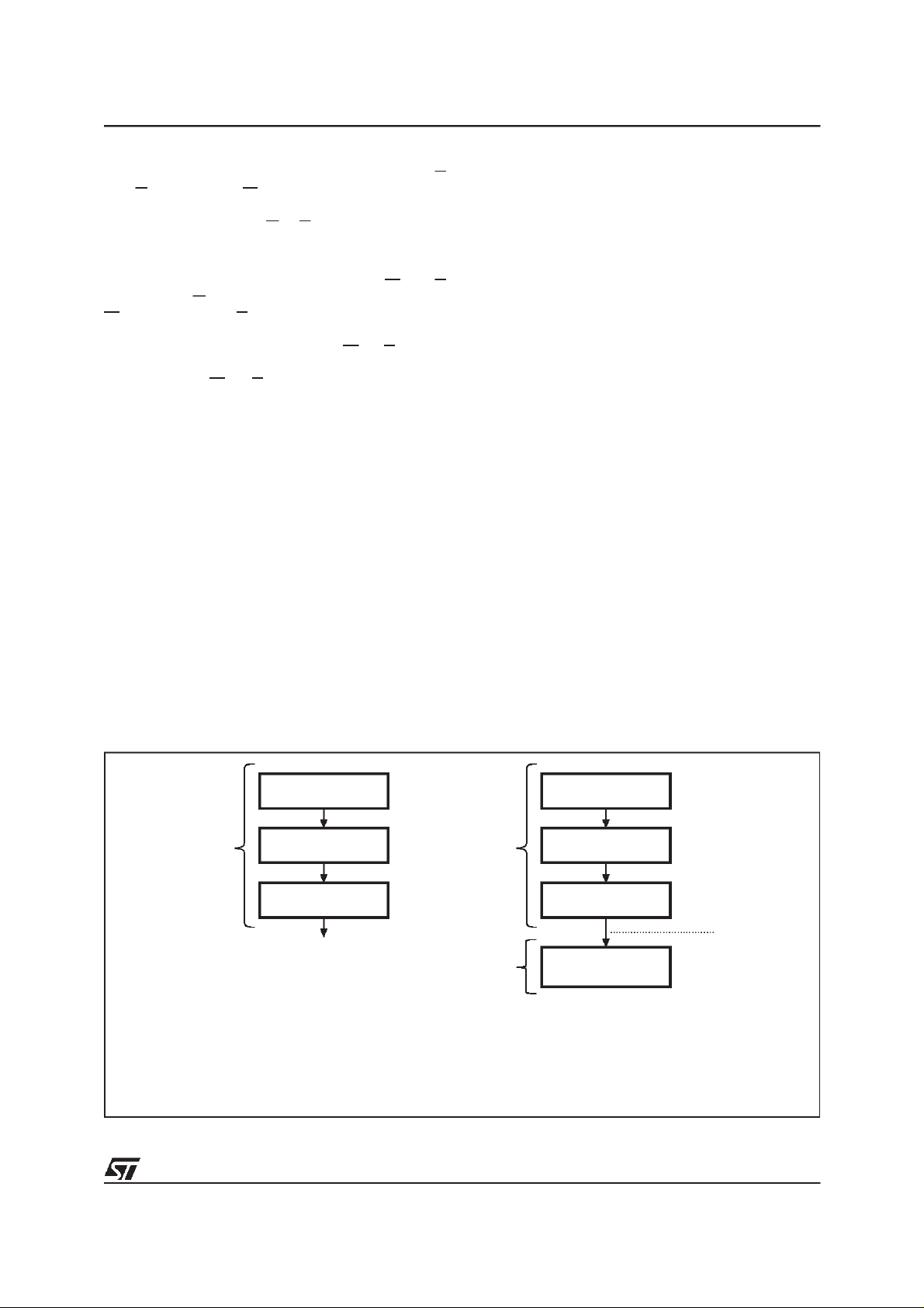
Software Data Protection (SDP)
The device offers a software-controlled writeprotection mechanism that allows the user to
inhibit all write operations to the device. This can
be useful for protecting the memory from
inadvertent write cycles that may occur during
periods of instability (uncontrolled bus conditions
when excessive noise is detected,or when power
supply levels are outside their specified values).
By default, the device is shipped in the
“unprotected” state: the memory contents can be
freely changed by the user. Once the Software
Data Protection Mode is enabled, all write
commands are ignored,and have no effecton the
memory contents.
The device remains in this mode until a valid
Software Data Protection disable sequence is
received. The device reverts to its “unprotected”
state.
The status of the Software Data Protection
(enabled or disabled) is represented by a non-
Figure 4. Software Data Protection Enable Algorithm and Memory Write
Write AAh in
Address 1555h
Page Write
Timing
(see note 1)
Note: 1. The most significant address bits (A12 to A6) differ during these specific Page Write operations.
Write 55h in
Address 0AAAh
Write A0h in
Address 1555h
SDP is set
SDP Enable Algorithm
Page Write
Timing
(see note 1)
Physical
Page Write
Instruction
Write AAh in
Address 1555h
Write 55h in
Address 0AAAh
Write A0h in
Address 1555h
Page Write
(1 up to 64 bytes)
Write to
When SDP is SET
Memory
AI01356C
Write
is enabled
5/24
M28C64
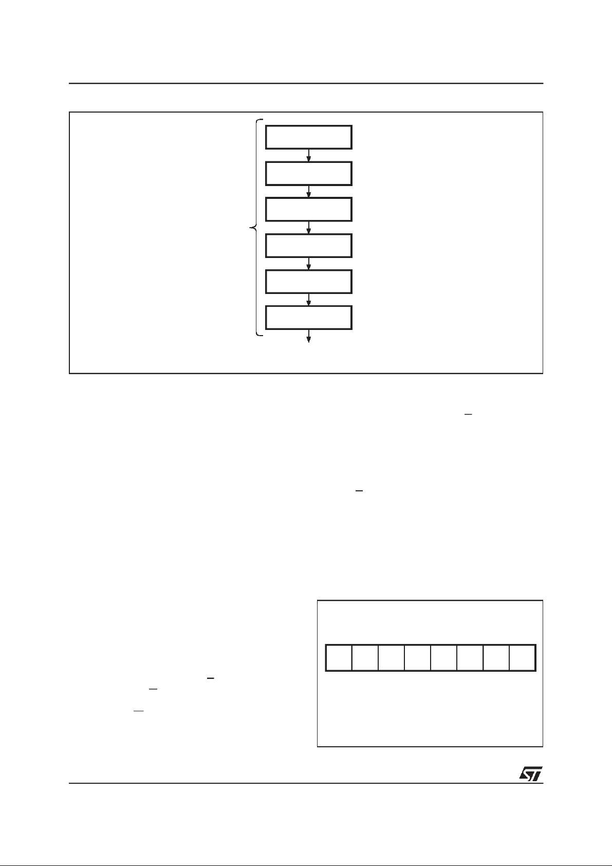
Figure 5. Software Data Protection Disable Algorithm
Write AAhin
Address 1555h
Write 55h in
Address 0AAAh
Write 80h in
Page Write
Timing
Address 1555h
Write AAhin
Address 1555h
Write 55h in
Address 0AAAh
Write 20h in
Address 1555h
Unprotected State
AI01357B
volatile latch, and is remembered across periods
of the power being off.
The Software Data Protection Enable command
consists of the writing of three specific data bytes
to three specific memory locations (each location
being on a different page), as shown in Figure 4.
Similarly to disable the Software Data Protection,
the user has to write specific data bytes into six
different locations, as shown in Figure 5. This
complex series of operations protects against the
chance of inadvertent enabling or disabling of the
Software Data Protection mechanism.
When SDP is enabled, the memoryarray can still
have data written to it, but the sequence is more
complex (and hence better protected from
inadvertent use). The sequence is as shown in
Figure 4. This consists of anunlock key, to enable
the write action, at the end of which the SDP
continues to be enabled. This allows the SDP to
be enabled, and data to be written, within a single
Write cycle (tWC).
Software Chip Erase
Using this function, available on the M28C64 but
not on the M28C64-A or M28C64-xxW, the
contents of the entire memory are erased (set to
FFh) by holding Chip Enable (E) low, and holding
Output Enable (G) at VCC+7.0V. The chip is
cleared when a 10 ms low pulse is applied to the
Write Enable (W) signal (seeFigure 7 and Table 5
for details).
Status Bits
The devices provide three status bits (DQ7, DQ6
and DQ5), and one output pin (RB), foruse during
write operations. These allow the application to
use the write time latency of the device for getting
on with other work. These signals areavailable on
the I/O port bits DQ7, DQ6 and DQ5 (but only
during programming cycle, once a byte or more
has been latched into the memory)or continuously
on the RB output pin.
Data Polling bit (DQ7). Theinternally timed write
cycle starts after t
WLQ5H
(defined in Table 10A to
Table 10C) has elapsed since the previous byte
was latched in to the memory. The value of the
DQ7 bit of this last byte, is used as a signal
Figure 6. Status Bit Assignment
DQ7 DQ6 DQ5 DQ4 DQ3 DQ2 DQ1 DQ0
DP TB PLTS Hi-Z Hi-Z Hi-Z Hi-Z Hi-Z
DP
= Data
TB
PLTS
Hi-Z
Polling
= Toggle Bit
= Page Load Timer
= High impedance
Status
AI02815
6/24
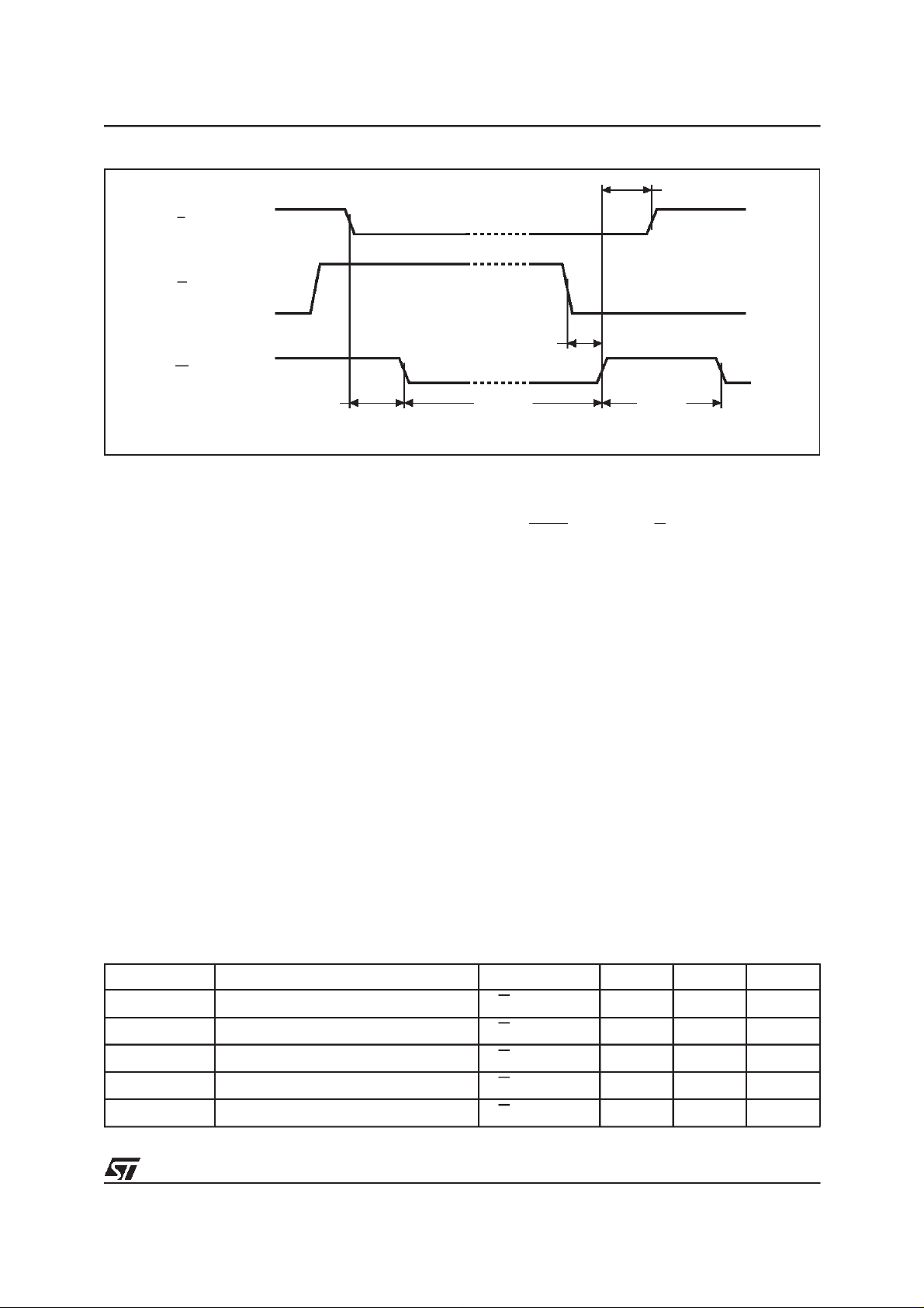
Figure 7. Chip Erase AC Waveforms (M28C64 and M28C64-xxW)
E
G
tGLWH
W
M28C64
tWHEH
throughout this write operation: it is inverted while
the internal write operation is underway, and is
inverted back to its original value once the
operation is complete.
Toggle bit (DQ6). The device offers another way
for determining when the internal write cycle is
completed. During the internal Erase/Write cycle,
DQ6 toggles from ’0’ to ’1’ and ’1’ to ’0’ (the first
read value being ’0’) on subsequent attempts to
read any byte of the memory. When the internal
write cycle is complete, the toggling is stopped,
and the valuesread on DQ7-DQ0are those ofthe
addressed memory byte. This indicates that the
device is again available for new Read and Write
operations.
Page Load Timer Status bit (DQ5). An internal
timer is used to measure the period between
successive Write operations, up to t
WLQ5H
(defined in Table 10Ato Table 10C). The DQ5 line
is held low to show when this timer is running
(hence showing that the device has received one
write operation, and is waiting for the next). The
DQ5 line is held high when the counter has
tWLWH2tELWL
tWHRH
AI01484B
overflowed (hence showingthat the device is now
starting the internal write to the memory array).
Ready/Busy pin. The RB pin is an open drain
output that isheld low duringthe erase/write cycle,
and that is released (allowed to float) at the
completion of the programming cycle.
Table 5. Chip Erase AC Characteristics1for M28C64 and M28C64-xxW
(TA= 0 to70 °C or –40 to 85 °C or –40 to 125 °C; VCC= 4.5 to 5.5 V)
(TA= 0 to 70 °C or –40 to 85 °C; VCC= 2.7 to 3.6 V)
Symbol Parameter Test Condition Min. Max. Unit
t
ELWL
t
WHEH
t
WLWH2
t
GLWH
t
WHRH
Note: 1. Sampled only, not 100% tested.
Chip Enable Low to Write Enable Low
Write Enable High to Chip Enable High G = VCC+7V 0 ns
Write Enable Low to Write Enable High
Output Enable Low to Write Enable High
Write Enable High to WriteEnable Low G = VCC+7V 3 ms
G=V
G=V
G=V
CC
CC
CC
+7V
+7V
+7V
1 µs
10 ms
1 µs
7/24
M28C64
Table 6A. Read Mode DC Characteristics for M28C64 and M28C64-A (5V range)
(TA= 0 to70 °C or –40 to 85 °C or –40 to 125 °C; VCC= 4.5 to 5.5 V)
Symbol Parameter Test Condition Min. Max. Unit
I
Input Leakage Current 0 V ≤ VIN≤ V
LI
I
I
CC
I
CC1
I
CC2
V
V
V
V
Note: 1. All inputs and outputs open circuit.
Output Leakage Current 0 V ≤ V
LO
Supply Current (TTL inputs) E = VIL,G=VIL, f = 5 MHz 30 mA
1
Supply Current (CMOS inputs)
1
Supply Current (Stand-by) TTL
1
Supply Current (Stand-by) CMOS E > VCC- 0.3V 100 µA
Input Low Voltage -0.3 0.8 V
IL
Input High Voltage 2
IH
Output Low Voltage
OL
Output High Voltage IOH= -400 µA 2.4 V
OH
E=V
,G=VIL, f = 5 MHz
IL
E=V
I
= 2.1 mA
OL
OUT
IH
≤ V
CC
CC
Table 6B. Read Mode DC Characteristics for M28C64-xxW (3V range)
(TA= 0 to70 °C or –40 to 85 °C; VCC= 2.7 to 3.6 V)
Symbol Parameter Test Condition Min. Max. Unit
I
Input Leakage Current
LI
I
I
CC
I
CC2
V
V
V
V
Note: 1. All inputs and outputs open circuit.
Output Leakage Current 0 V ≤ V
LO
1
Supply Current (CMOS inputs)
1
Supply Current (Stand-by) CMOS E > VCC- 0.3V 20 µA
Input Low Voltage -0.3 0.6 V
IL
Input High Voltage 2
IH
Output Low Voltage IOL= 1.6 mA 0.2 V
OL
Output High Voltage IOH= -400 µA 0.8 V
OH
E=V
E=V
0V≤ V
,G=VIL, f = 5 MHz, VCC= 3.3V 8 mA
IL
,G=VIL, f = 5 MHz, VCC= 3.6V 10 mA
IL
IN
OUT
≤ V
≤ V
CC
CC
CC
10 µA
10 µA
25 mA
1mA
V
+ 0.5
CC
0.4 V
10 µA
10 µA
V
+ 0.5
CC
CC
V
V
V
V
8/24
 Loading...