

ST M27C4001 User Manual
查询M27C4001-10N1X供应商
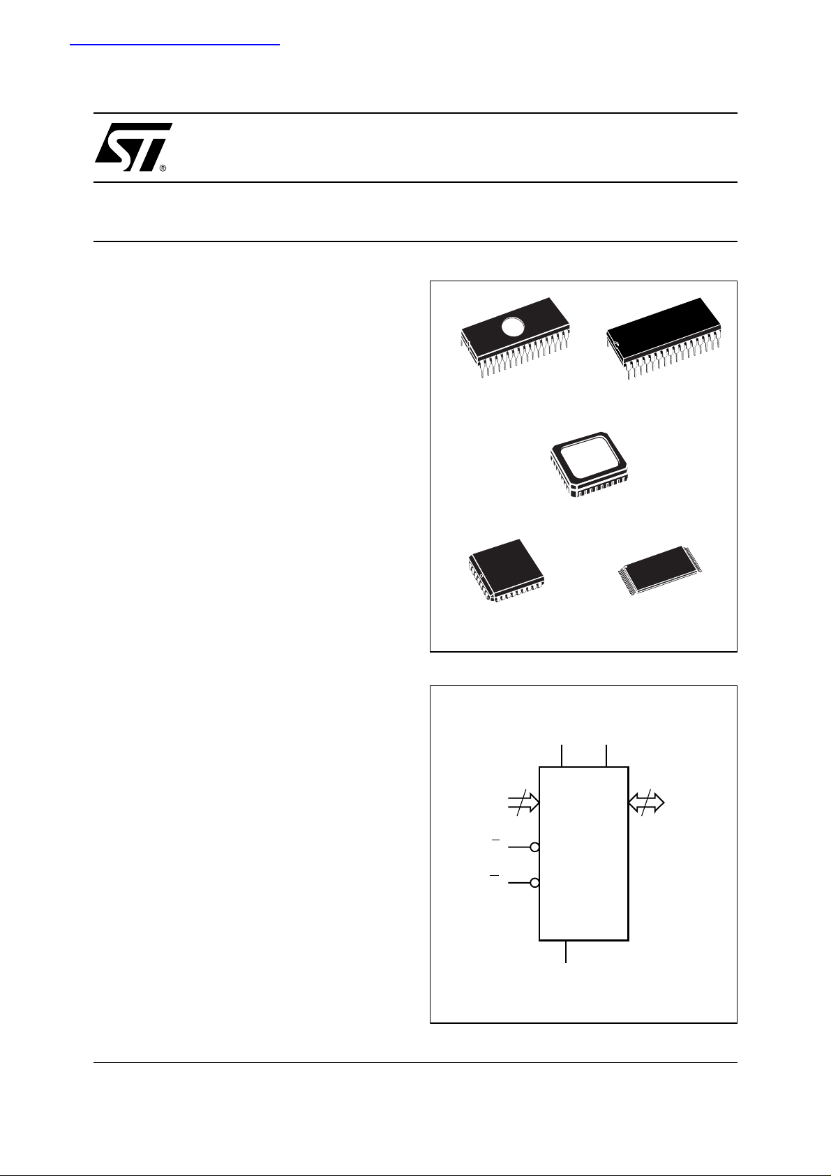
4 Mbit (512Kb x 8) UV EPROM and OTP EPROM
■ 5V ± 10% SUPPLY VOLTAGE in READ
OPERATION
■ ACCESS TIME: 35ns
■ LOW POWER CONSUMPTION:
– Active Current 30mA at 5MHz
– Standby Current 100µA
■ PROGRAMMING VOLTAGE: 12.75V ± 0.25V
■ PROGRAMMING TIME: 100µs/word
■ ELECTRONIC SIGNATURE
– Manufacturer Code: 20h
– Device Code: 41h
DESCRIPTION
The M27C4001 is a 4 Mbit EPROM offered in the
two ranges UV (ultra violet erase) and OTP (one
time programmable). It is ideally suited for microprocessor systems requiring large programs and
is organised as 524,288 by 8 bits.
The FDIP32W (window ceramic frit-seal package)
and LCCC32W (leadless chip carrier package)
have a transparent lid which allow the user to expose the chip to ultraviolet light to erase the bit pattern. A new pattern can then be written to the
device by following the programming procedure.
For applications where the content is programmed
only one time and erasure is not required, the
M27C4001 is offered in PDIP32, PLCC32 and
TSOP32 (8 x 20 mm) packages.
M27C4001
32
1
FDIP32W (F)
LCCC32W (L)
PLCC32 (C)
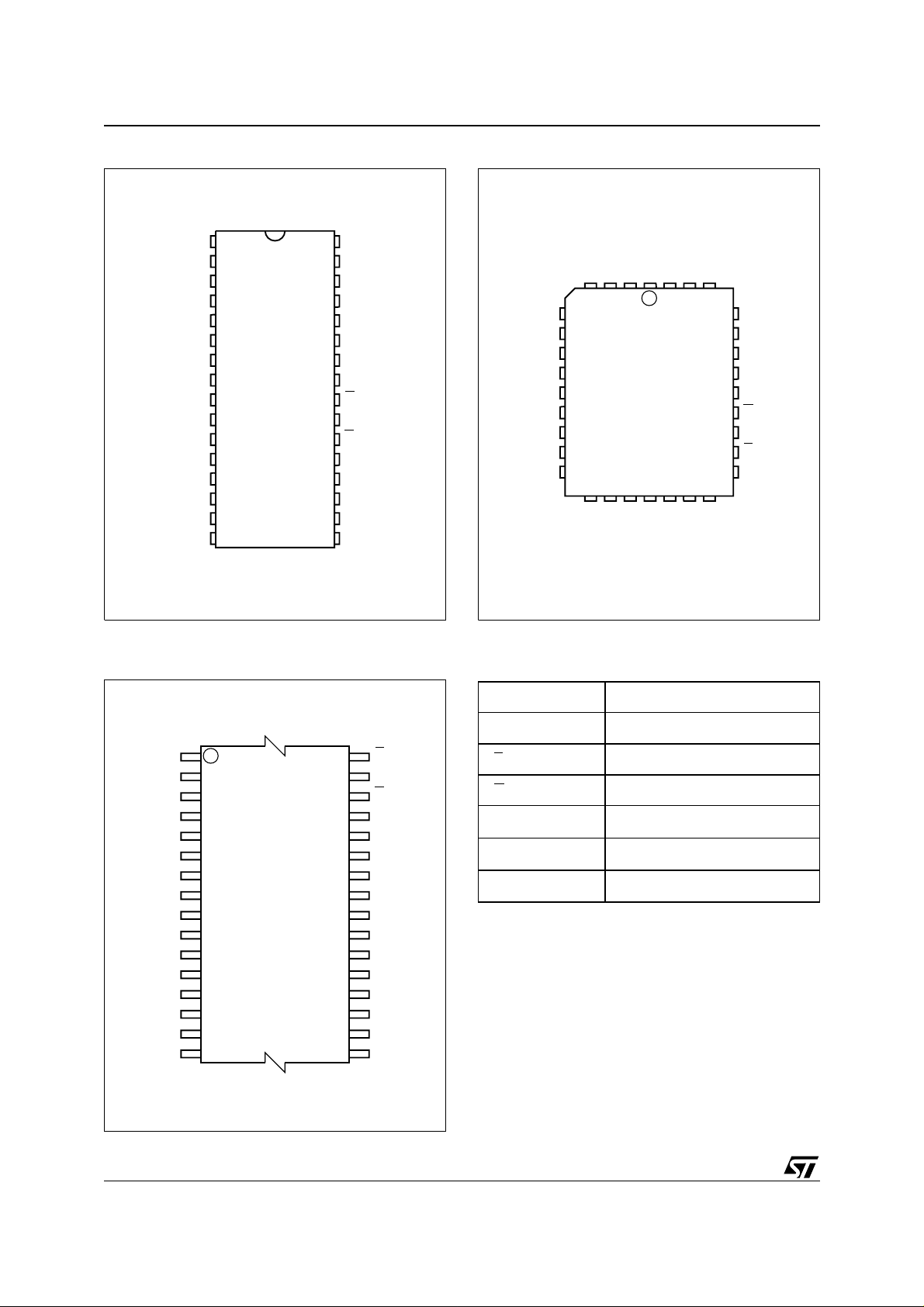
Figure 1. Logic Diagram
V
19
A0-A18 Q0-Q7
CC
32
V
PP
1
PDIP32 (B)
TSOP32 (N)
8 x 20 mm
8
E
G
M27C4001
V
SS
AI00721B
1/17November 2000
M27C4001
Figure 2A. DIP Connections
V
1
PP
2
A15
3
A12
4
5
A7
6
A6
7
A5
8
A4
A3
A2
A1
A0
Q0
Q2
SS
M27C4001
9
10
11
12
13
14
15
16
32
31
30
29
28
27
26
25
24
23
22
21
20
19
18
17
AI00722
V
CC
A18A16
A17
A14
A13
A8
A9
A11
G
A10
E
Q7
Q6
Q5Q1
Q4
Q3V
Figure 2B. LCC Connections
A16
A7
A6
A5
A4
A3
A2
A1
A0
Q0
A12
9
Q1
VPPV
A15
1
32
M27C4001
17
Q2
Q3
SS
V
Q4
CC
A18
Q5
A17
25
Q6
A14
A13
A8
A9
A11
G
A10
E
Q7
AI00723
Figure 2C. TSOP Connections
A11 G
A9
A8
A13
A14
A17
A18
V
CC
V
PP
A16
A15
A12
A7
A6
A5
A4 A3
1
M27C4001
8
(Normal)
9
16 17
AI01155B
32
25
24
A10
E
Q7
Q6
Q5
Q4
Q3
V
SS
Q2
Q1
Q0
A0
A1
A2
Table 1. Signal Names
A0-A18 Address Inputs
Q0-Q7 Data Outputs
E
G
V
PP
V
CC
V
SS
Chip Enable
Output Enable
Program Supply
Supply Voltage
Ground
2/17
M27C4001
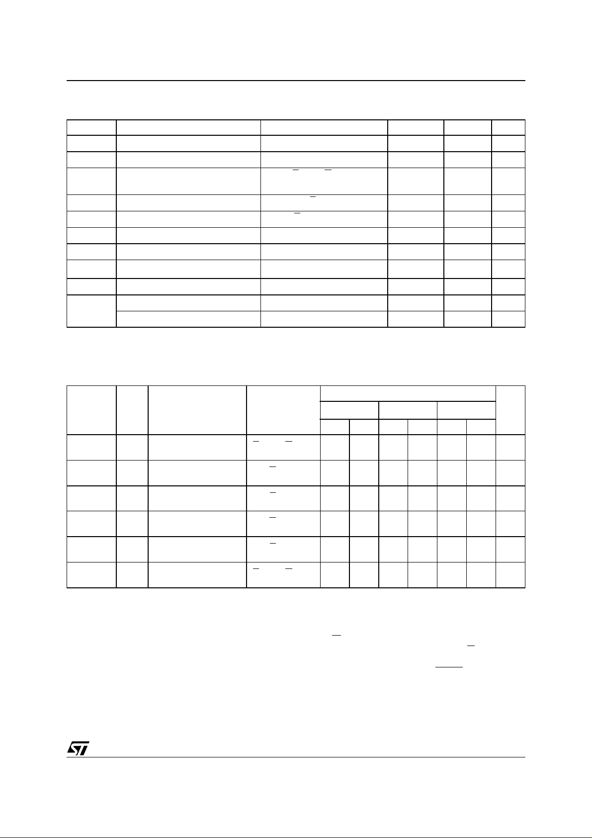
Table 2. Absolute Maximum Ratings
(1)
Symbol Parameter Value Unit
T
A
T
BIAS
T
STG
(2)
V
IO
V
CC
(2)
V
A9
V
PP
Note: 1. Except for the ratin g " Operating Temperature Range", stresses abo ve those listed in the T able "Abs ol ute Maximum Ratings" may
cause permanent damage to the device. These are stress ratings only and operation of the device at these or any other conditions
above those indi cated in the Operating sections of this s pecification is not impli ed. Exposure to A bsolute Maximum Rating conditions for extended per iods may aff ect device reliabilit y. Refer also to the STMicroel ectronics SURE Program an d other relevan t qual ity docum en ts .
2. Min imum DC volta ge on In put or O utput is –0.5V with po ssible under shoot t o –2.0V f or a period less th an 20ns. Maximu m DC
voltage on Output is V
3. Depends on range.
Table 3. Operating Modes
Ambient Operating Temperature
Temperature Under Bias –50 to 125 °C
Storage Temperature –65 to 150 °C
Input or Output Voltage (except A9) –2 to 7 V
Supply Voltage –2 to 7 V
A9 Voltage –2 to 13.5 V
Program Supply Voltage –2 to 14 V
+0.5V with possible overshoot to VCC +2V for a period l ess than 20n s.
CC
(1)
Mode E
Read
Output Disable
Program
Verify
Program Inhibit
Standby
Electronic Signature
Note: 1. X = VIH or VIL, VID = 12V ± 0.5V.
V
IL
V
IL
V
Pulse V
IL
V
IH
V
IH
V
IH
V
IL
(3)
G A9
V
IL
V
IH
IH
V
IL
V
IH
X
X
X
X
X
XX
V
IL
V
ID
–40 to 125 °C
V
pp
V
or V
CC
SS
V
or V
CC
SS
V
PP
V
PP
V
PP
V
or V
CC
SS
V
CC
Q7 - Q0
Data Out
Hi-Z
Data In
Data Out
Hi-Z
Hi-Z
Codes
Table 4. Electronic Signature
Identifier A0 Q7 Q6 Q5 Q4 Q3 Q2 Q1 Q0 Hex Data
Manufacturer’s Code
Electronic Signature
V
IL
V
IH
00100000 20h
01000001 41h
3/17
M27C4001
Table 5. AC Measurement Conditions
High Speed Standard
Input Rise and Fall Times
Input Pulse Voltages 0 to 3V 0.4 to 2.4V
Input and Output Timing Ref. Voltages 1.5V 0.8 and 2V
10ns
≤
20ns
≤
Figure 3. AC Testing Input Output Waveform
High Speed
3V
1.5V
0V
Standard
2.4V
0.4V
Table 6. Capacitance
Symbol Parameter Test Condition Min Max Unit
C
IN
C
OUT
Note: 1. Sampled only, not 100% tested.
(1)
(TA = 25 °C, f = 1 MHz)
Input Capacitance
Output Capacitance
2.0V
0.8V
AI01822
Figure 4. AC Testing Load Circuit
1.3V
DEVICE
UNDER
TEST
CL = 30pF for High Speed
CL = 100pF for Standard
CL includes JIG capacitance
V
= 0V
IN
V
= 0V
OUT
1N914
3.3kΩ
CL
6pF
12 pF
OUT
AI01823B
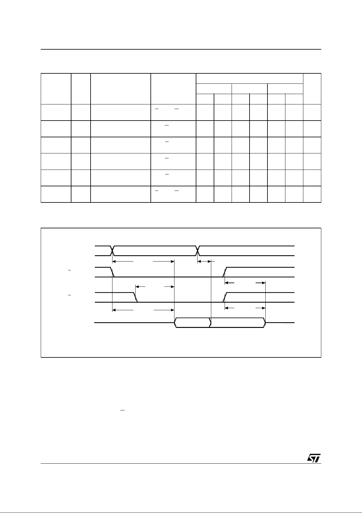
DEVICE OPERATION
The operating modes of the M 27C4001 are list ed
in the Operating Modes table. A single power supply is required in the read mode. All inputs are TTL
levels except for V
and 12V on A9 for Electronic
PP
Signature.
Read Mode
The M27C4001 has t wo control functions, both of
which must be logically ac tive in order to obtain
data at the output s. Chip Enable (E
) is the power
control and should be used for device selection.
Output Enable (G
) is the output control and should
be used to gate data to the output pins, independent of device selection. Assuming that the ad-
4/17
dresses are stable, the address access time
) is equal to the delay from E to output
(t
AVQV
(t
). Data is available at the output after a delay
ELQV
of t
E
ble for at least t
from the falling edge of G, assum ing that
GLQV
has been low and the addresses have been sta-
AVQV-tGLQV
.
Standby Mode
The M27C4001 has a standby mode which reduces the supply current from 30mA to 100µA. The
M27C4001 is place d in the standby m ode by applying a CMOS high signal to the E
input. When in
the standby mode, the outputs are in a high impedance state, independent of the G
input.
M27C4001
Table 7. Read Mode DC Characteristics
(1)
(TA = 0 to 70 °C or –40 to 85 °C; VCC = 5V ± 5% or 5V ± 10%; VPP = VCC)
Symbol Parameter Test Condition Min Max Unit
I
OUT
0V ≤ V
0V ≤ V
E
E
I
I
I
LI
I
LO
I
CC
I
CC1
I
CC2
I
PP
V
V
IH
V
OL
V
OH
Note: 1. VCC must be ap pl i e d simultaneously wi t h or before VPP and removed simultaneously or af ter VPP.
2. Max imum DC voltage on Output is V
Table 8A. Read Mode AC Characteristics
Input Leakage Current
Output Leakage Current
Supply Current
Supply Current (Standby) TTL
Supply Current (Standby) CMOS
Program Current
Input Low Voltage –0.3 0.8 V
IL
(2)
Input High Voltage 2
Output Low Voltage
Output High Voltage TTL
Output High Voltage CMOS
+0.5 V.
CC
(1)
≤ V
IN
CC
≤ V
OUT
CC
= VIL, G = VIL,
= 0mA, f = 5MHz
E
= V
IH
> VCC – 0.2V
V
= V
PP
CC
I
= 2.1mA
OL
= –400µA
OH
= –100µAV
OH
2.4 V
– 0.7V
CC
±10
±10
30 mA
1mA
100
10
V
+ 1
CC
0.4 V
(TA = 0 to 70 °C or –40 to 85 °C; VCC = 5V ± 5% or 5V ± 10%; VPP = VCC)
M27C4001
Symbol Alt Parameter Test Condition
-35
(3)
Min Max Min Max Min Max
Address Valid to
(2)
(2)
t
ACC
Output Valid
Chip Enable Low to
t
CE
Output Valid
Output Enable Low to
t
OE
Output Valid
Chip Enable High to
t
DF
Output Hi-Z
Output Enable High to
t
DF
Output Hi-Z
Address Transition to
t
OH
Output Transition
t
AVQV
t
ELQV
t
GLQV
t
EHQZ
t
GHQZ
t
AXQX
Note: 1. VCC must be ap pl i e d simultaneously wi t h or before VPP and removed simultaneously or af ter V
2. Sampled only, not 100% tested.
3. Speed obtained with High Speed AC measurement condition s.
= VIL, G = V
E
= V
G
= V
E
= V
G
= V
E
= VIL, G = V
E
IL
IL
IL
IL
IL
IL
35 45 55 ns
35 45 55 ns
20 25 30 ns
030030030ns
030030030ns
000ns
-45
(3)
PP
-55
(3)
A
µ
A
µ
A
µ
A
µ
V
V
Unit
Two Line Outp ut C ontrol
Because EPROMs are usually used in larger
memory arrays, this product features a 2 line control function which accommodates the use of multiple memory connection. The two line control
function allows:
a. the lowest possible memory power dissipation,
b. complete assurance that output bus contention
will not occur.
For the most efficient use of these two control
lines, E
ry device selecting function, while G
should be decoded and used as the prima-
should be
made a common connectio n to all devices in the
array and connected to the READ
line from the
system control bus. This ensures that all deselected memory devices are in their low power standby
mode and that the output pins are only active
when data is required from a particular memory
device.
5/17
M27C4001
Table 8B. Read Mode AC Characteristics
(1)
(TA = 0 to 70 °C or –40 to 85 °C; VCC = 5V ± 5% or 5V ± 10%; VPP = VCC)
M27C4001
Symbol Alt Parameter Test Condition
Min Max Min Max Min Max
t
AVQV
t
ELQV
t
GLQV
(2)
t
EHQZ
(2)
t
GHQZ
t
AXQX
Note: 1. VCC must be ap pl i e d simultaneously wi t h or before VPP and removed simultaneously or af ter VPP.
2. Sampled only, not 100% tested.
Address Valid to
t
ACC
Output Valid
Chip Enable Low to
t
CE
Output Valid
Output Enable Low to
t
OE
Output Valid
Chip Enable High to
t
DF
Output Hi-Z
Output Enable High to
t
DF
Output Hi-Z
Address Transition to
t
OH
Output Transition
= VIL, G = V
E
= V
G
= V
E
= V
G
= V
E
= VIL, G = V
E
IL
IL
IL
IL
IL
IL
70 80 100 ns
70 80 100 ns
35 40 50 ns
030030030ns
030030030ns
000ns
Figure 5. Read Mode AC Waveforms
Unit-70 -80/-90 -10/-12/-15
A0-A18
E
G
Q0-Q7
VALID
tAVQV
tGLQV
tELQV
System Considerations
The power switching characteristics of Advanced
CMOS EPROMs require careful decoupling of the
devices. The supply current, I
, has three seg-
CC
ments that are of interest to the system designe r:
the standby current level, the active current level,
and transient current peaks that are p roduced by
the falling and rising edges of E
. The magnitude of
the transient current peaks is dependent on the
capacitive and inductive loading of the device at
the output. The associated transient voltage peaks
can be suppres sed by complying with th e two line
VALID
tAXQX
tEHQZ
tGHQZ
Hi-Z
AI00724B
output control and by properly selected decoupling
capacitors. It is recommended that a 0.1µF ceramic capacitor be used on every device between V
CC
and VSS. This should be a high frequency capac itor of low inherent inductance and should be
placed as close to the device as possible. In addition, a 4.7 µF bulk electrolytic capacitor should be
used between V
and VSS for every eight devic-
CC
es. The bulk capacitor sho uld be located near the
power supply connection point. The purpose of the
bulk capacitor is to overcome the voltage drop
caused by the inductive effects of PCB traces.
6/17
 Loading...