

查询M27C2001-10B1TR供应商
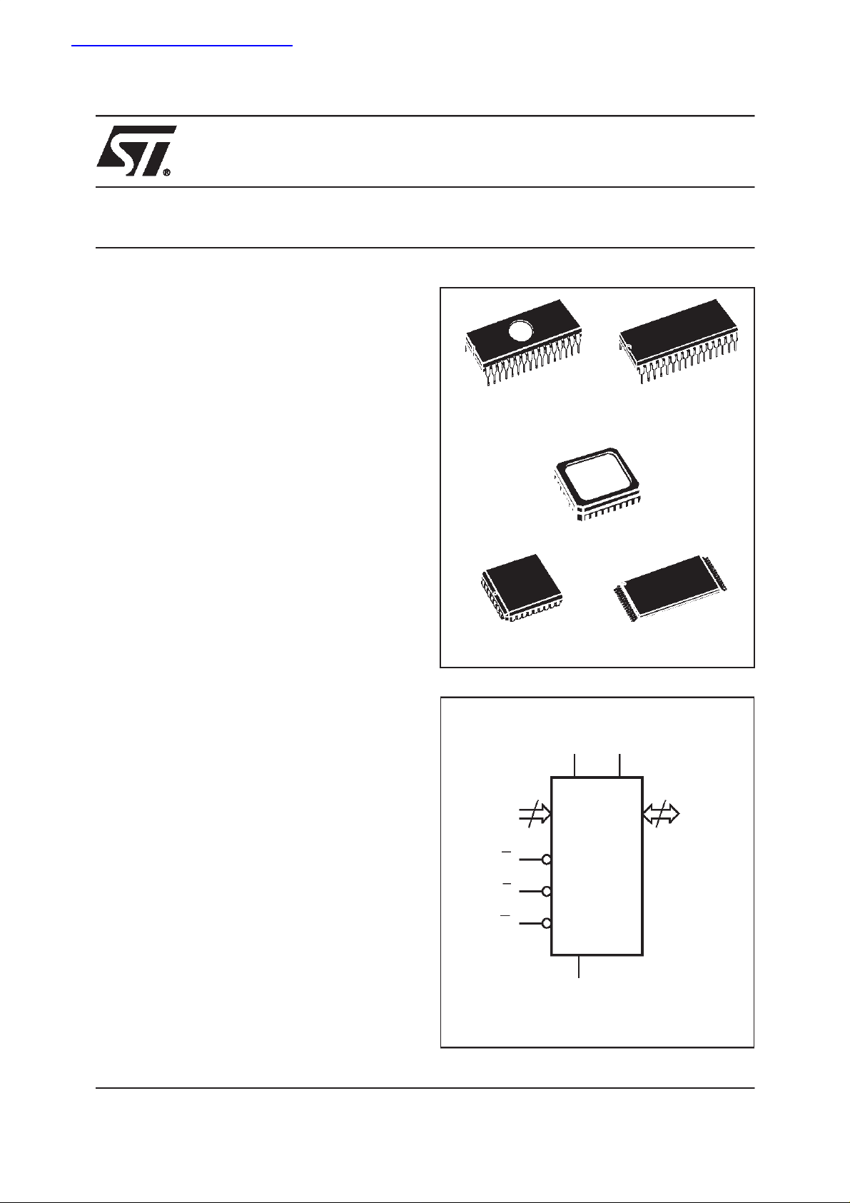
2 Mbit (256Kb x 8) UV EPROM and OTP EPROM
■ 5V ± 10% SUPPLY VOLTAGE in READ
OPERATION
■ ACCESS TIME: 55ns
■ LOW POWER CONSUMPTION:
– Active Current 30mA at 5MHz
– Standby Current 100µA
■ PROGRAMMING VOLTAGE: 12.75V ± 0.25V
■ PROGRAMMING TIME: 100µs/word
■ ELECTRONIC SIGNATURE
– Manufacturer Code: 20h
– Device Code: 61h
M27C2001
32
1
FDIP32W (F) PDIP32 (B)
32
1
DESCRIPTION
The M27C2001 is a high speed 2 Mbit EPROM offered inthetwo ranges UV (ultraviolet erase) and
OTP (one time programmable). It is ideally suited
for microprocessor systems requiring large programs and is organised as 262,144 by 8 bits.
The FDIP32W (window ceramic frit-seal package)
and LCCC32W (leadless chip carrier package)
have atransparent lidswhich allow the user to expose the chipto ultraviolet light to erase the bitpattern. A new pattern can then be written to the
device by following the programming procedure.
For applications where the contentis programmed
only one time and erasure is not required, the
M27C2001 is offered in PDIP32, PLCC32 and
TSOP32 (8 x 20 mm) packages.
LCCC32W (L)
PLCC32 (C) TSOP32 (N)
Figure 1. Logic Diagram
V
CC
18
A0-A17
P
E
G
M27C2001
V
8 x 20 mm
PP
8
Q0-Q7
V
SS
AI00716B
1/17November 2000
M27C2001
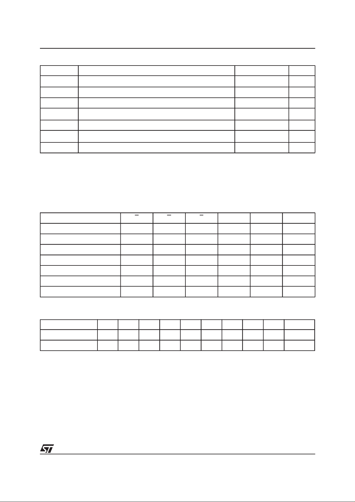
Figure 2A. DIP Connections
V
1
PP
2
A15
3
A12
4
A7
5
A6
6
A5
7
A4
8
A3
A2
A1
A0
Q0
Q2
SS
M27C2001
9
10
11
12
13
14
15
16
32
31
30
29
28
27
26
25
24
23
22
21
20
19
18
17
AI00717
V
CC
PA16
A17
A14
A13
A8
A9
A11
G
A10
E
Q7
Q6
Q5Q1
Q4
Q3V
Figure 2B. LCC Connections
A16
A7
A6
A5
A4
A3
A2
A1
A0
Q0
A12
9
Q1
VPPV
A15
1
32
M27C2001
17
Q2
Q3
SS
V
Q4
CC
P
Q5
A17
25
Q6
A14
A13
A8
A9
A11
G
A10
E
Q7
AI00718
Figure 2C. TSOP Connections
A11 G
A9
A8
A13
A14
A17
V
CC
V
PP
A16
A15
A12
A7
A6
A5
A4 A3
1
P
M27C2001
8
(Normal)
9
16 17
AI01153B
32
25
24
A10
E
Q7
Q6
Q5
Q4
Q3
V
SS
Q2
Q1
Q0
A0
A1
A2
Table 1. Signal Names
A0-A17 Address Inputs
Q0-Q7 Data Outputs
E Chip Enable
G Output Enable
P Program
V
PP
V
CC
V
SS
Program Supply
Supply Voltage
Ground
2/17
M27C2001
Table 2. Absolute Maximum Ratings
(1)
Symbol Parameter Value Unit
T
A
T
BIAS
T
STG
(2)
V
IO
V
CC
(2)
V
A9
V
PP
Note: 1. Except for the rating ”Operating Temperature Range”, stresses above those listedin the Table ”Absolute Maximum Ratings” may
cause permanent damage to the device. These are stress ratings only and operation of the device at these or any other conditions
above those indicated in the Operating sections of this specification is not implied. Exposure toAbsolute Maximum Rating conditions for extended periods may affect device reliability. Refer also to the STMicroelectronics SURE Program andotherrelevant quality documents.
2. Minimum DC voltage on Input or Output is –0.5V with possible undershoot to –2.0V for a period less than 20ns. Maximum DC
voltage on Output is V
3. Depends on range.
Ambient Operating Temperature
Temperature Under Bias –50 to 125 °C
Storage Temperature –65 to 150 °C
Input or Output Voltage (except A9) –2 to 7 V
Supply Voltage –2 to 7 V
A9 Voltage –2 to 13.5 V
Program Supply Voltage –2 to 14 V
+0.5V with possible overshoot to VCC+2V for a period less than 20ns.
CC
(3)
–40 to 125 °C
Table 3. Operating Modes
Mode E G P A9
Read
Output Disable V
Program
Verify V
Program Inhibit
Standby
Electronic Signature
Note: X = VIHor VIL,VID= 12V ± 0.5V.
V
IL
IL
V
IL
IL
V
IH
V
IH
V
IL
V
IL
V
IH
V
IH
V
IL
XX
XXV
VILPulse
V
IH
X
XVPPData Out
XXX
XXX
V
IL
V
IH
V
ID
V
PP
V
or V
CC
SS
or V
CC
SS
V
PP
V
PP
V
or V
CC
SS
V
CC
Q7-Q0
Data Out
Hi-Z
Data In
Hi-Z
Hi-Z
Codes
Table 4. Electronic Signature
Identifier A0 Q7 Q6 Q5 Q4 Q3 Q2 Q1 Q0 Hex Data
Manufacturer’s Code
Device Code
V
IL
V
IH
00100000 20h
01100001 61h
3/17
M27C2001
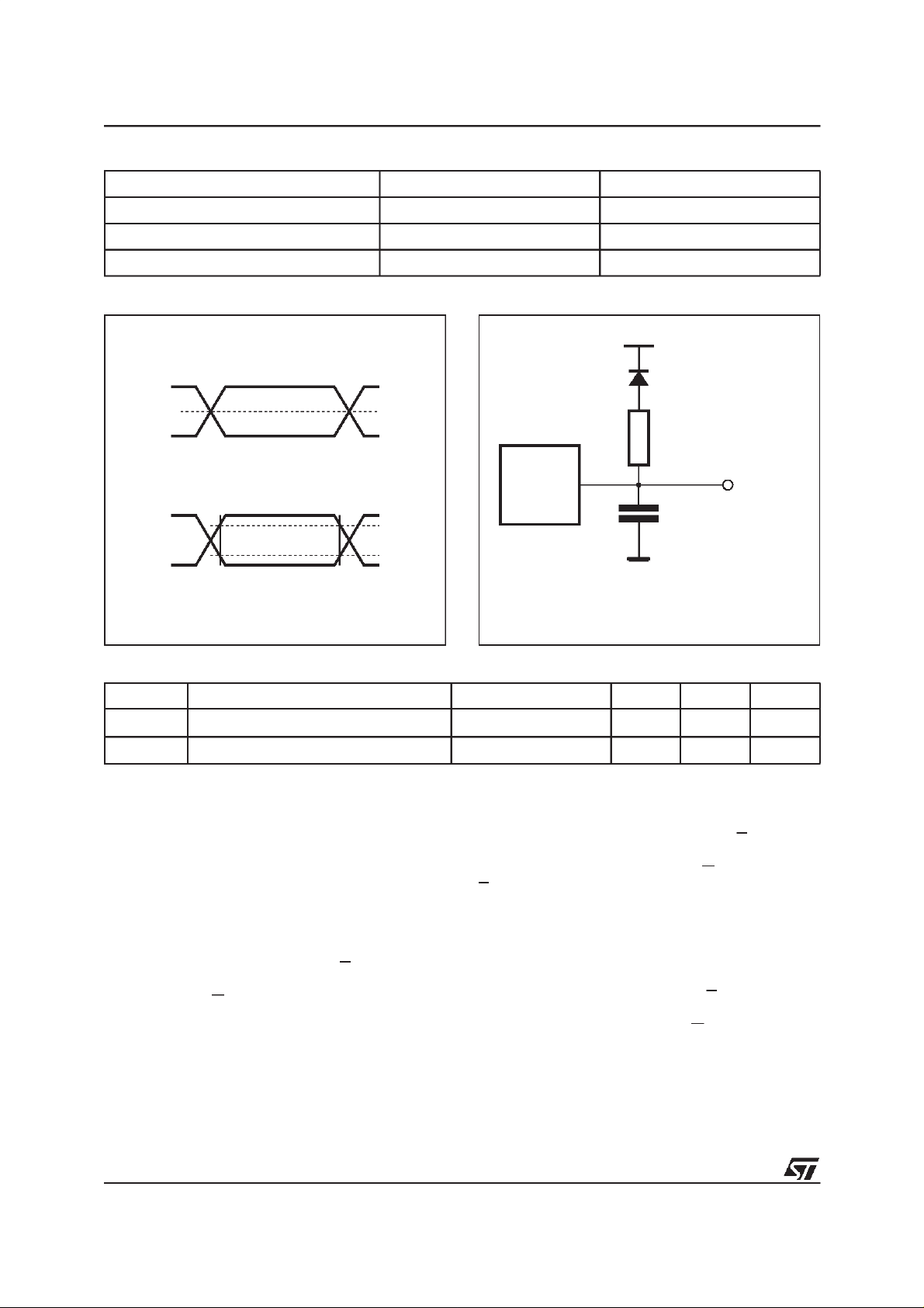
Table 5. AC Measurement Conditions
High Speed Standard
Input Rise and Fall Times ≤ 10ns ≤ 20ns
Input Pulse Voltages 0 to 3V 0.4V to 2.4V
Input and Output Timing Ref. Voltages 1.5V 0.8V and 2V
Figure 3. AC Testing Input Output Waveform
High Speed
3V
1.5V
0V
Standard
2.4V
0.4V
Table 6. Capacitance
Symbol Parameter Test Condition Min Max Unit
C
IN
C
OUT
Note: 1. Sampled only,not 100% tested.
Input Capacitance
Output Capacitance
(1)
(TA=25°C, f = 1 MHz)
2.0V
0.8V
AI01822
Figure 4. AC Testing Load Circuit
1.3V
1N914
3.3kΩ
DEVICE
UNDER
TEST
C
L
CL= 30pF for HighSpeed
CL= 100pF for Standard
CLincludes JIG capacitance
V
V
IN
OUT
=0V
=0V
6pF
12 pF
OUT
AI01823B
DEVICE OPERATION
The operating modes of the M27C2001 are listed
in the Operating Modes table. A single powersupply is required in theread mode. All inputs areTTL
levels except for VPPand 12V on A9 for Electronic
Signature.
Read Mode
The M27C2001 has two control functions, both of
which must be logically active in order to obtain
data at the outputs. Chip Enable (E) is the power
control and should be used for device selection.
Output Enable (G) is theoutput control and should
be used to gate data to the output pins, indepen-
4/17
dent of device selection. Assuming that the addresses are stable, the address access time
(t
) is equal to the delay from E to output
AVQV
(t
). Datais available at the output after a delay
ELQV
of t
from the falling edge of G, assuming that
GLQV
E has been low and the addresses have been stable for at least t
AVQV-tGLQV
.
Standby Mode
The M27C2001 has a standbymode whichreduces the supply current from 30mA to 100µA. The
M27C2001 is placed in the standby mode by applying a CMOS high signal to the E input.When in
the standby mode, the outputs are in a high impedance state, independent of the G input.
M27C2001
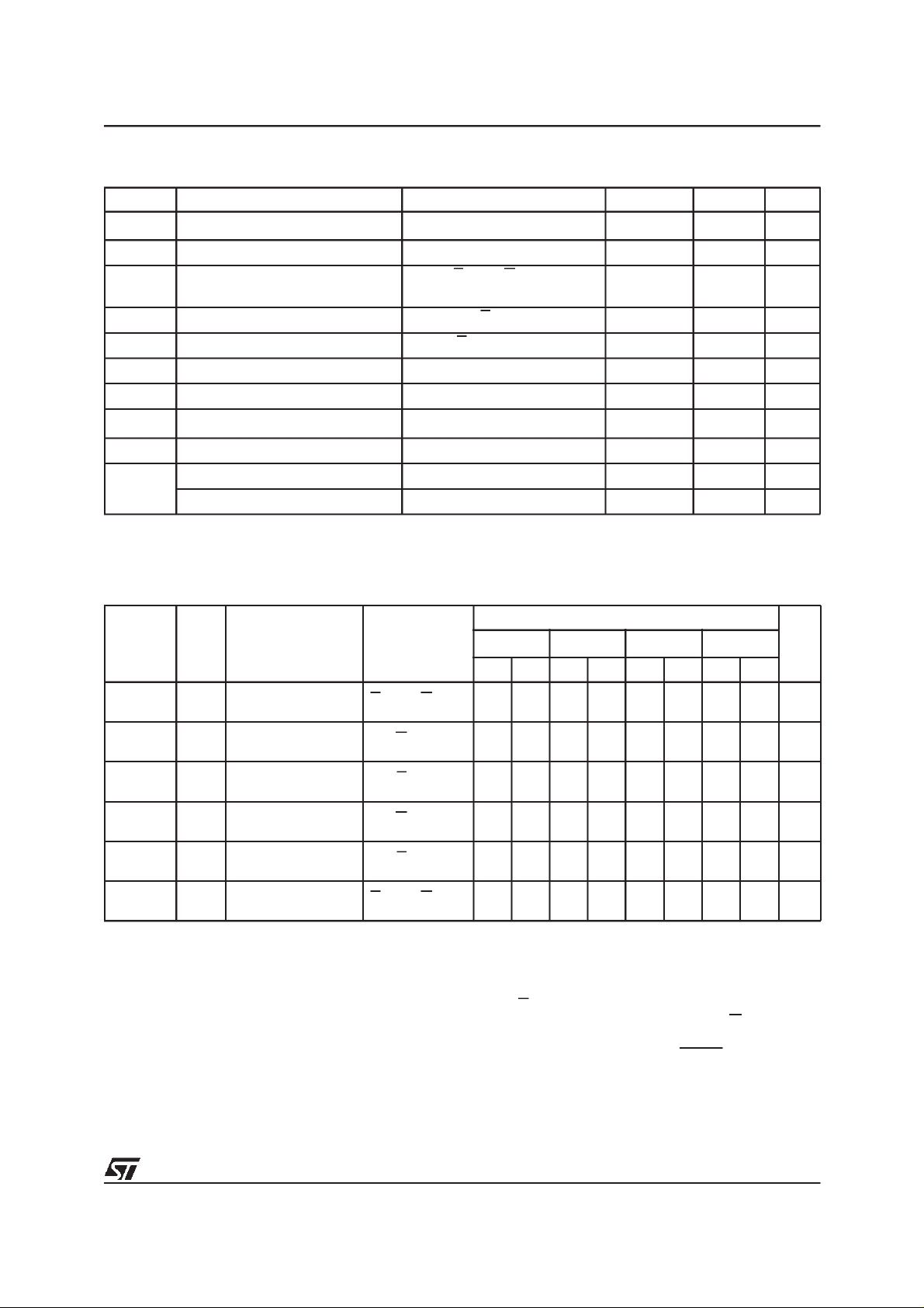
Table 7. Read Mode DC Characteristics
(1)
(TA = 0 to 70 °C or –40 to 85 °C; VCC=5V±5% or 5V ± 10%; VPP=VCC)
Symbol Parameter Test Condition Min Max Unit
I
I
I
CC
I
CC1
I
CC2
I
V
V
IH
V
V
Note: 1. VCCmust be applied simultaneously with or before VPPand removed simultaneously or after VPP.
Table 8A. Read Mode AC Characteristics
Input Leakage Current
LI
Output Leakage Current 0V ≤ V
LO
Supply Current
Supply Current (Standby) TTL
I
OUT
0V ≤ V
E=V
≤ V
IN
CC
≤ V
OUT
CC
,G=VIL,
IL
= 0mA,f = 5MHz
E=V
IH
Supply Current (Standby) CMOS E > VCC– 0.2V 100 µA
Program Current
PP
Input Low Voltage –0.3 0.8 V
IL
(2)
Input High Voltage 2
Output Low Voltage
OL
Output High VoltageTTL
OH
Output High VoltageCMOS
2. Maximum DC voltage on Output is V
CC
+0.5V.
(1)
V
PP=VCC
I
= 2.1mA
OL
I
= –400µA
OH
= –100µAV
I
OH
CC
2.4 V
– 0.7V
±10 µA
±10 µA
30 mA
1mA
10 µA
V
+1
CC
0.4 V
(TA = 0 to 70 °C or –40 to 85 °C; VCC=5V±5% or 5V ± 10%; VPP=VCC)
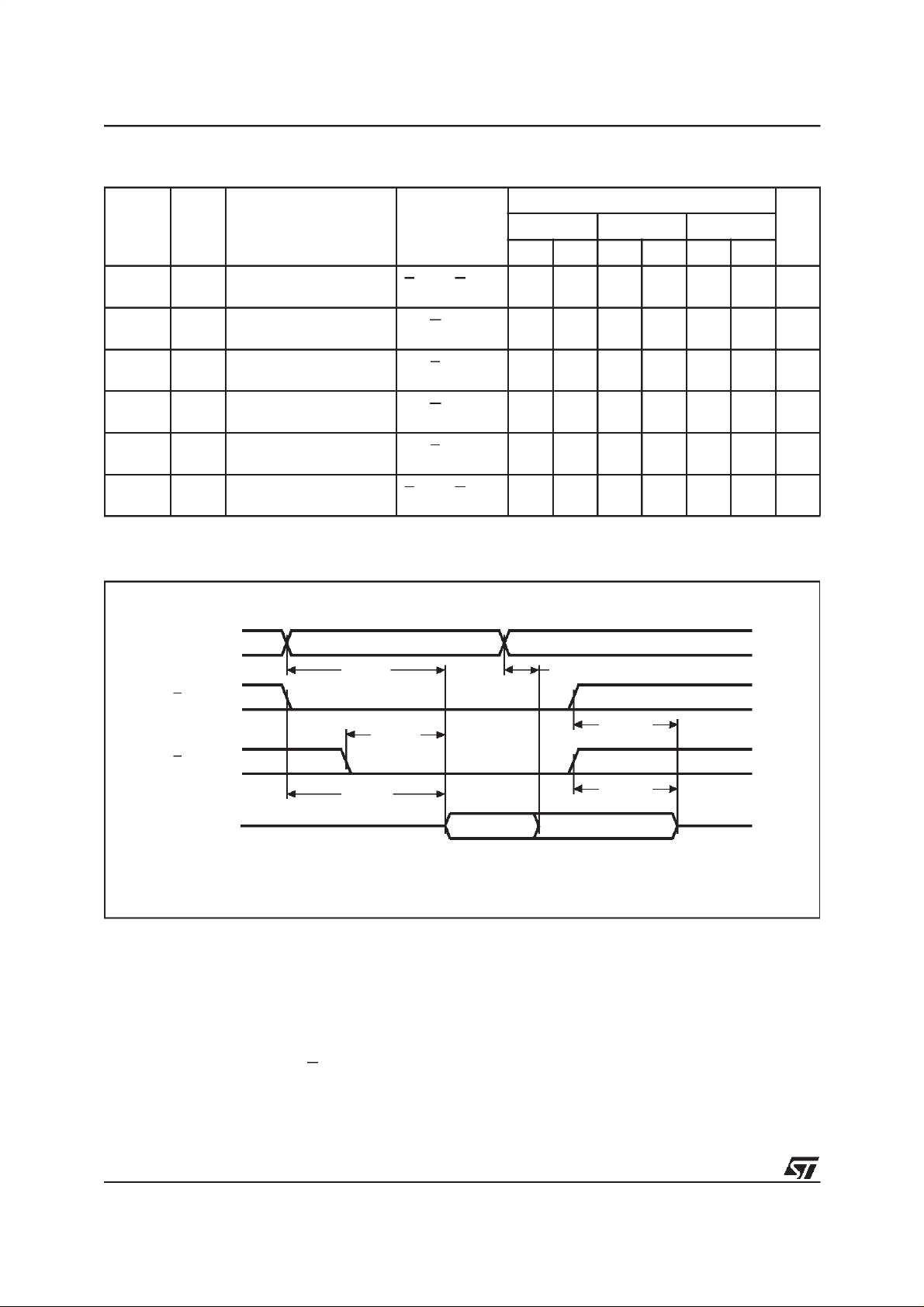
M27C2001
Symbol Alt Parameter Test Condition
-55
(3)
Min Max Min Max Min Max Min Max
Address Valid to
(2)
(2)
t
ACC
Output Valid
Chip EnableLow to
t
CE
Output Valid
Output Enable Low
t
OE
to Output Valid
Chip EnableHigh to
t
DF
Output Hi-Z
Output Enable High
t
DF
to Output Hi-Z
Address Transitionto
t
OH
Output Transition
t
AVQV
t
ELQV
t
GLQV
t
EHQZ
t
GHQZ
t
AXQX
Note: 1. VCCmust be applied simultaneously with or before VPPand removed simultaneously or after VPP.
2. Sampled only, not 100% tested.
3. In case of 45ns speed see High Speed AC measurement conditions.
E=V
G=V
G=V
E=V
,G=V
IL
E=V
E=V
,G=V
IL
IL
IL
IL
IL
IL
IL
55 70 80 90 ns
55 70 80 90 ns
30 35 40 40 ns
0 30 0 30 0 30 0 30 ns
0 30 0 30 0 30 0 30 ns
0000ns
-70 -80 -90
V
V
Unit
Two Line Output Control
Because EPROMs are usually used in larger
memory arrays, this product features a 2 line control function which accommodates the use of multiple memory connection. The two line control
function allows:
a. the lowest possible memory power dissipation,
b. complete assurance that output bus contention
will not occur.
For the most efficient use of these two control
lines, Eshould be decodedand used as the primary device selecting function, while G should be
made a common connection to all devices in the
array and connected to the READ line from the
system control bus. This ensures that all deselected memory devices are intheir lowpower standby
mode and that the output pins are only active
when data is required from a particular memory
device.
5/17
M27C2001
Table 8B. Read Mode AC Characteristics
(1)
(TA = 0 to 70 °C or –40 to 85 °C; VCC=5V±5% or 5V ± 10%; VPP=VCC)
M27C2001
Symbol Alt Parameter Test Condition
Min Max Min Max Min Max
t
AVQV
t
ELQV
t
GLQV
t
EHQZ
t
GHQZ
t
AXQX
Note: 1. VCCmust be applied simultaneously with or before VPPand removed simultaneously or after VPP.
t
(2)
(2)
2. Sampled only, not 100% tested.
Address Valid to Output
ACC
Valid
Chip EnableLow to
t
CE
Output Valid
Output Enable Low to
t
OE
Output Valid
Chip EnableHigh to
t
DF
Output Hi-Z
Output Enable High to
t
DF
Output Hi-Z
Address Transition to
t
OH
Output Transition
E=V
E=V
,G=V
IL
G=V
E=V
G=V
E=V
,G=V
IL
IL
IL
IL
IL
IL
IL
100 120 150 ns
100 120 150 ns
50 50 60 ns
030040050ns
030040050ns
000ns
Figure 5. Read Mode AC Waveforms
Unit-10 -12 -15/-20/-25
A0-A17
E
G
Q0-Q7
VALID
tAVQV
tGLQV
tELQV
System Considerations
The power switching characteristics of Advanced
CMOS EPROMs requirecareful decoupling of the
devices. The supply current, ICC, has three segments that are of interest to the system designer:
the standby current level, the active current level,
and transient current peaks that are produced by
the falling and rising edges of E. The magnitude of
the transient current peaks is dependent on the
capacitive and inductive loading of the device at
the output. The associated transient voltage peaks
can besuppressed by complying with the two line
VALID
tAXQX
tEHQZ
tGHQZ
Hi-Z
AI00719B
outputcontrol and byproperly selected decoupling
capacitors.It is recommended that a 0.1µFceramic capacitorbe used on every device between V
CC
and VSS. This should be a high frequency capacitor of low inherent inductance and should be
placed as close to the device aspossible. In addition, a 4.7µF bulk electrolytic capacitor should be
used between VCCand VSSfor every eight devices. The bulk capacitor should be located near the
power supply connection point. The purpose of the
bulk capacitor is to overcome the voltage drop
caused by the inductive effects of PCB traces.
6/17
 Loading...