

ST M27C160 User Manual
查询M27C160-100F1供应商
16 Mbit (2Mb x 8 or 1Mb x 16) UV EPROM and OTP EPROM
■ 5V ± 10% SUPPLY VOLTAGE in READ
OPERATION
■ ACCESS TIME: 50ns
■ BYTE-WID E or WORD-WIDE
CONFIGURABLE
■ 16 Mbit MASK ROM REPLACEMENT
■ LOW P OWER CONSUMPTION
– Active Current 70mA at 8MHz
– Standby Current 100µA
■ PROGRAMMING VOLTAGE: 12.5V ± 0.25V
■ PROG RAMM ING T IME: 50µs/word
■ ELECTRONIC SIGNATURE
– Manufacturer Code: 20h
– Device Code: B1h
42
1
FDIP42W (F)
M27C160
42
1
PDIP42 (B)
42
1
SDIP42 (S)
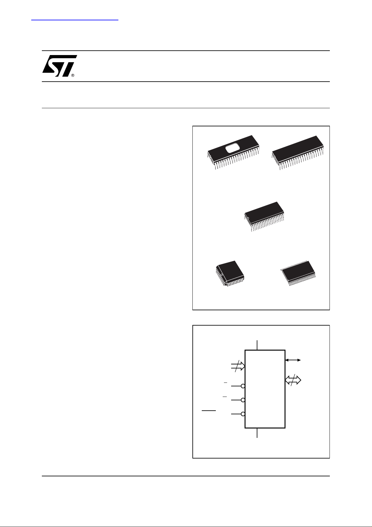
DESCRIPTION
The M27C160 is a 16 Mbit EPROM offered in the
two ranges UV (ultra violet erase) and OTP ( one
time programmable). It is ideally suited for microprocessorsystemsrequiringlarge data or program
storage and is organised as either 2 Mb it words of
8 bit or 1 Mbit words of 16 bit. The pin-out is compatible with a 16 Mbit Mask ROM.
The FDIP42W (window ceramic frit-seal package)
has a transparent lid whi ch allows the user to expose the chip to ultraviolet light to erase the bit pattern. A new pattern can then be written rapidly to
the device by following the p rogramm ing procedure.
For applications where the content is programmed
only one time and erasure is not required, the
M27C160 is offered in PDIP42, SDIP42, PLCC44
and SO44 packages.
PLCC44 (K)
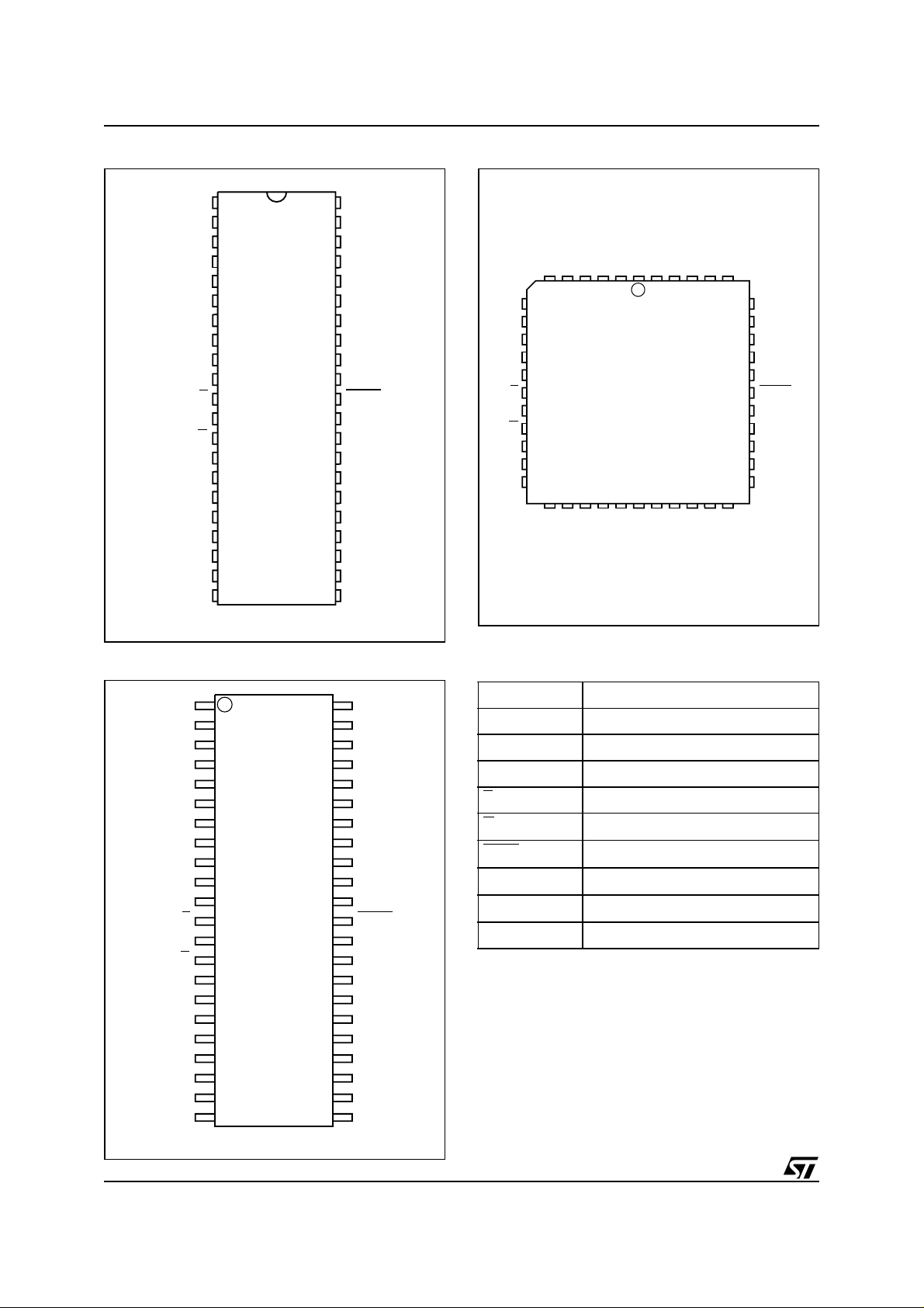
Figure 1. Logic Diagram
V
CC
20
A0-A19
BYTEV
E
G
PP
M27C160
V
SS
44
1
SO44 (M)
Q15A–1
15
Q0-Q14
AI00739B
1/19January 2002
M27C160
Figure 2. DIP Connections
A18 A19
1
2
A7
3
4
A6
5
A5
A4
6
7
A3
A2
8
A1
9
10
A0
V
SS
Q0
Q8
Q1
Q9
Q10
Q3
Q11
E
G
11
12
13
14
15
16
17
18
19
20
21
M27C160
42
41
40
39
38
37
36
35
34
33
32
31
30
29
28
27
26
25
24
23
22
AI00740
A8A17
A9
A10
A11
A12
A13
A14
A15
A16
BYTEV
V
SS
Q15A-1
Q7
Q14
Q6
Q13
Q5Q2
Q12
Q4
V
CC
PP
Figure 3. PLCC Connections
A18
A17
V
1
M27C160
23
Q3
NC
Q11
SS
44
A19
CC
V
A8
Q4
A9
Q12
A10
Q5
A7
A5
A6
A4
A3
A2
A1 A15
A0
E
12
V
SS
Q0
Q8
Q1
Q9
Q2
Q10
A11
34
Q13
A12
A13
A14
A16
BYTEV
V
SS
Q15A–1G
Q7
Q14
Q6
AI03012
PP
Figure 4. SO Connections
NC NC
A17 A8
V
SS
Q0
Q8
Q9
Q10
Q3
Q11
A7
A6
A5
A4
A3
A2
A1
A0
1
2
3
4
5
6
7
8
9
10
11
M27C160
12
E
13
14
G
15
16
17Q1
18
19
20
21
44
43
42
41
40
39
38
37
36
35
34
33
32
31
30
29
28
27
26
25
24
2322
AI01264
A19A18
A9
A10
A11
A12
A13
A14
A15
A16
BYTEV
V
SS
Q15A-1
Q7
Q14
Q6
Q13
Q5Q2
Q12
Q4
V
CC
PP
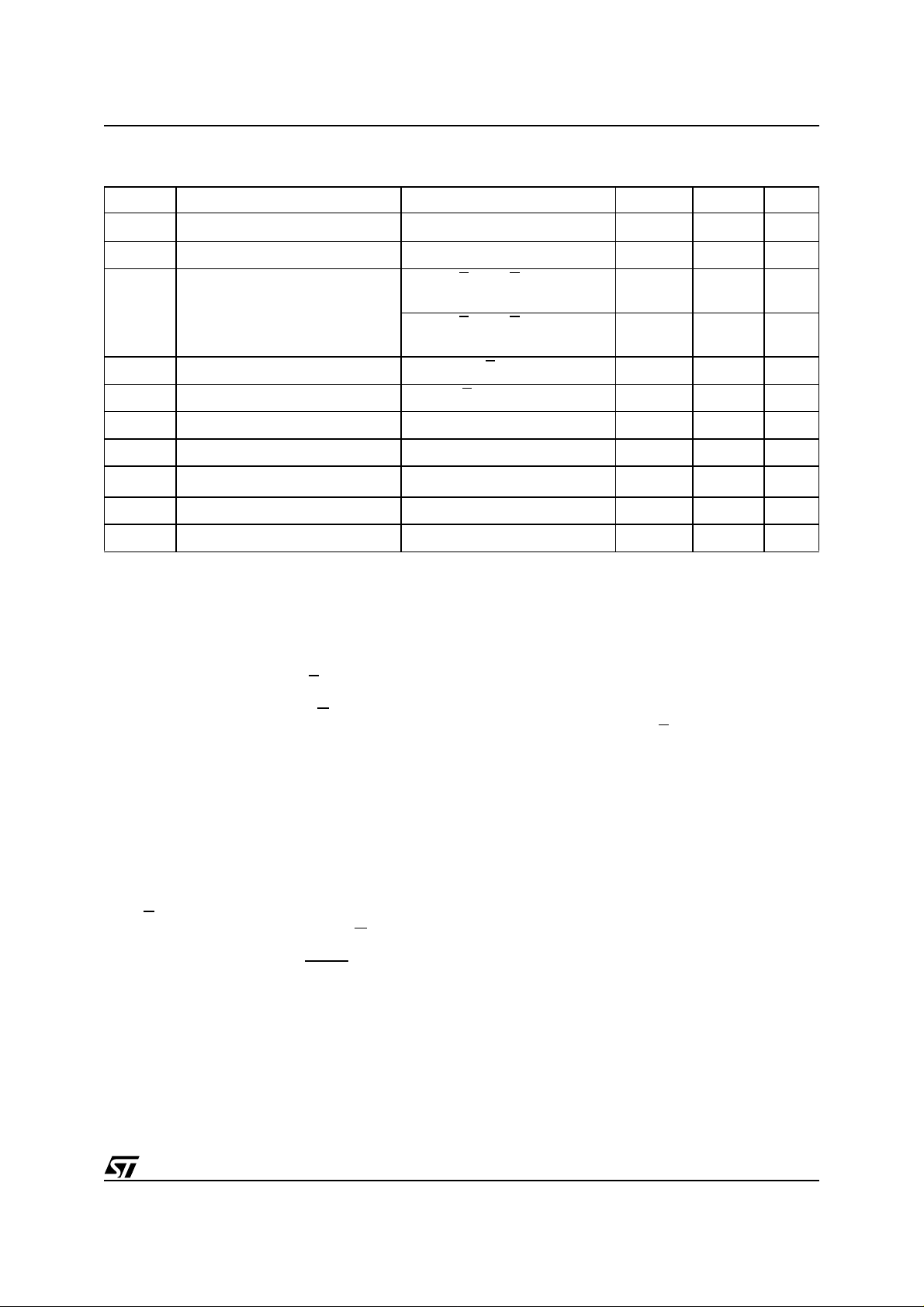
Table 1. Signal Names
A0-A19 Address Inputs
Q0-Q7 Data Outputs
Q8-Q14 Data Outputs
Q15A–1 Data Output / Address Input
E
G
BYTE
V
PP
V
CC
V
SS
NC Not Connected Internally
Chip Enable
Output Enable
Byte Mode / Program Supply
Supply Voltage
Ground
2/19
M27C160
Table 2. Absolute Maximum Ratings
(1)
Symbol Parameter Value Unit
T
A Ambient Operating Temperature
T
BIAS
T
STG
(2)
V
IO
V
CC
(2)
V
A9
V
PP
Note: 1. Except for the rating "Operating Temperature Range", stresses above those listed in the Table "Absolute Maximum Ratings" may
cause permanent damage to the device. These are stress ratings only and operation of the device at these or any other conditions
above those indicated in the Operating sections of this specification is not implied. Exposure to Absolute Maximum Rating conditionsfor extended periods may affectdevice reliability. Referalsoto the STMicroelectronics SUREProgramandother relevant quality documents.
2. Minimum DC voltage on Input or Output is –0.5V with possible undershoot to –2.0V for a period less than 20ns. Maximum DC
voltage on Output is V
3. Depends on range.
Temperature Under Bias –50 to 125 °C
Storage Temperature –65 to 150 °C
Input or Output Voltage (except A9) –2 to 7 V
Supply Voltage –2 to 7 V
A9 Voltage –2 to 13.5 V
Program Supply Voltage –2 to 14 V
+0.5VwithpossibleovershoottoVCC+2V for a period less than 20ns.
CC
(3)
–40 to 125 °C
Table 3. Operating Modes
Mode E
Read Word-wide
Read Byte-wide Upper
Read Byte-wide Lower
Output Disable
Program
V
Verify
Program Inhibit
Standby
Electronic Signature
Note: X = VIHor VIL,VID= 12V ± 0.5V.
V
IL
V
IL
V
IL
V
IL
Pulse V
IL
V
IH
V
IH
V
IH
V
IL
G
V
V
V
V
V
V
X X X Hi-Z Hi-Z Hi-Z
V
BYTEV
PP
IL
IL
IL
IH
IH
IL
IH
IL
V
IH
V
IL
V
IL
X X Hi-Z Hi-Z Hi-Z
V
PP
V
PP
V
PP
V
IH
A9 Q15A–1 Q8-Q14 Q7-Q0
X Data Out Data Out Data Out
X
X
V
IH
V
IL
Hi-Z Data Out
Hi-Z Data Out
X Data In Data In Data In
X Data Out Data Out Data Out
X Hi-Z Hi-Z Hi-Z
V
ID
Code Codes Codes
Table 4. Electronic Signature
Identifier A0 Q7 Q6 Q5 Q4 Q3 Q2 Q1 Q0 Hex Data
Manufacturer’s Code
Device Code
Note: Outputs Q15-Q8 are set to '0'.
V
V
IL
IH
00100000 20h
10110001 B1h
3/19
M27C160
Table 5. AC M easurement Conditions
High Speed Standard
Input Rise and Fall Times ≤ 10ns ≤ 20ns
Input Pulse Voltages 0 to 3V 0.4V to 2.4V
Input and Output Timing Ref. Voltages 1.5V 0.8V and 2V
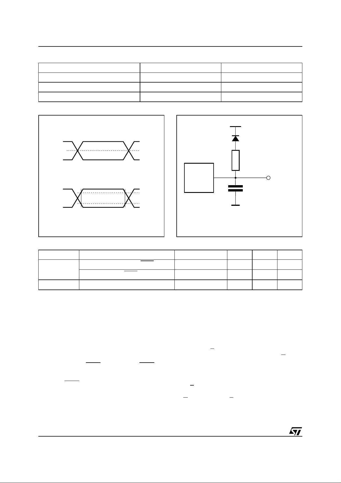
Figure 5. AC Testing Input Output Waveform
High Speed
3V
1.5V
0V
Standard
2.4V
0.4V
Table 6. Capacitance
Symbol Parameter Test Condition Min Max Unit
C
IN
C
OUT
Note: 1. Sampled only, not 100% tested.
(1)
(TA=25°C,f=1MHz)
Input Capacitance (except BYTEVPP)V
Input Capacitance (BYTE
Output Capacitance
2.0V
0.8V
AI01822
VPP)V
Figure 6. AC Testing Load Circuit
1.3V
1N914
3.3kΩ
DEVICE
UNDER
TEST
CL
CL = 30pF for High Speed
CL = 100pF for Standard
CL includes JIG capacitance
V
IN
IN
OUT
=0V
=0V
=0V
10 pF
120 pF
12 pF
OUT
AI01823B
DEVICE OPERATION
The operating modes of the M27C160 are listed in
the Operating Modes Table. A single power supply
is required in the read mode. All inputs are TTL
compatible except for V
and 12V on A9 for the
PP
Electronic Signature.
Read Mode
The M27C160 has two organisations, Word-wide
and Byte-wide. The organisation isselected by the
signal level on the BYTE
VPPpin. When BYTEV
PP
is at VIHthe Word-wide organisation is selected
and the Q15A–1 pin is used for Q15 Data Output.
When the BYTE
VPPpin is at VILthe Byte-wide organisation is selected and the Q15A–1 pin is used
for the Address In put A–1. When the memory is
logically regarded as 16 bit wide, but read in the
Byte-wide organisation, then with A–1 at V
4/19
the
IL
lower 8 bits of the 16 bit data are s elected and with
A–1 at V
the upper 8 bits of the 16 bit data are
IH
selected.
The M27C160 has tw o control func ti ons , both of
which mus t be logically active in order to obtain
data at the outputs. In addition the Word-wide or
Byte- wide organisation must be selected.
ChipEnable (E
used for device selection. Output Enable (G
) is the power control and should be
)isthe
output control and s hould be used to gate data to
the output pins independent of device selection.
Assuming that the addresses are st able, the address access time (t
from E
to output (t
ELQV
output after a delay of t
of G
, assuming that E has been low and the ad-
dresses have been s tab le for at least t
) is equal to the delay
AVQV
). Data is available at the
from the falling edge
GLQV
AVQV-tGLQV
.
M27C160
Table 7. Read Mode DC Characteristics
(1)
(TA=0to70°Cor–40to85°C;VCC= 5V ± 5% or 5V ± 10%; VPP=VCC)
Symbol Parameter Test Condition Min Max Unit
I
I
LO
I
CC
I
CC1
I
CC2
I
PP
V
V
IH
V
V
Note: 1. VCCmust be applied simultaneously with or before VPPand removed simultaneously or after VPP.
Input Leakage Current
LI
Output Leakage Current
Supply Current
Supply Current (Standby) TTL
Supply Current (Standby) CMOS
Program Current
Input Low Voltage –0.3 0.8 V
IL
(2)
Input High Voltage 2
Output Low Voltage
OL
Output High Voltage TTL
OH
2. Maximum DC voltage on Output is V
CC
+0.5V.
I
OUT
I
OUT
0V ≤ V
0V ≤ V
E
E
E
I
OH
≤ V
IN
CC
≤ V
OUT
=VIL,G=VIL,
= 0mA, f = 8MHz
=VIL,G=VIL,
= 0mA, f = 5MHz
E
>VCC– 0.2V
V
PP=VCC
I
= 2.1mA
OL
= –400µA
=V
CC
IH
2.4 V
±1 µA
±10 µA
70 mA
50 mA
1mA
100 µA
10 µA
V
+1
CC
0.4 V
V
Standby Mode
The M27C160 has a standby mode which reduces
the active current from 50mA to 100µA. The
M27C160 is placed in the standby mode by applying a CMOS high sig nal to the E
input. When in the
standby mode, the outputs are in a high impedance state, independent of the G
input.
Two Line Output Control
Because EPROMs are usually used in larger
memory arrays, this product features a 2 line control function which accommodates the use of multiple memory connection. The two line control
function allows:
a. the lowest possible memory power dissipation,
b. complete assurance that output bus contention
will not occur.
For the most efficient use of thes e two control
lines, E
ry device selecting function, while G
should be decoded and us ed as theprima-
should be
made a common connection to all devices in the
array and connected to the READ
line from the
system control bus. This ensures that all des elected memory devices are in their low power standby
mode and that the out put pins are only active
when data is required from a partic ular me mory
device.
System Considerations
The power switching characteristics of Advanced
CMOS EPROMs r equire careful decoupling of the
supplies to the de vice s. The supply current I
CC
has three segments of i mportance to the system
designer: t he standby current, the active current
and the transient peaks that a re produced by the
falling and rising edges of E
.
The magnitude of the transient current peak s is
dependent on the c apacitive and i nduc ti ve loading
of the device outputs. The associated trans ient
voltage peaks can be suppressed by compl ying
with th e two line output control and by properly selected decou pling capacitors. It is recommended
that a 0.1µF ceramic capacitor is used on every
device between V
and VSS. This should be a
CC
high frequency type of low inherent inductance
and should be placed as close as possible to the
device. In addition, a 4 .7µ F electrolytic c apacitor
should be used bet ween V
and VSSfor every
CC
eight devices.
This capacitor s hould be mounted near the power
supply connection point. The purpose of this capacitor is to overcome the v olt age drop caused by
the inductive effects of PCB traces.
5/19
M27C160
Table 8. Read Mode AC Characteristics
(1)
(TA=0to70°Cor–40to85°C;VCC= 5V ± 5% or 5V ± 10%; VPP=VCC)
M27C160
Symbol Alt Parameter Test Condition
Min Max Min Max
Address Valid to
(2)
(2)
(2)
t
ACC
Output Valid
BYTE High to Output
t
ST
Valid
Chip Enable Low to
t
CE
Output Valid
Output Enable Low to
t
OE
Output Valid
BYTE Low to Output
t
STD
Hi-Z
Chip Enable High to
t
DF
Output Hi-Z
Output Enable High to
t
DF
OutputHi-Z
Address Transition to
t
OH
Output Transition
BYTE Low to
t
OH
Output Transition
t
AVQV
t
BHQV
t
ELQV
t
GLQV
t
BLQZ
t
EHQZ
t
GHQZ
t
AXQX
t
BLQX
Note: 1. VCCmust be applied simultaneously with or before VPPand removed simultaneously or after V
2. Sampled only, not 100% tested.
3. Speed obtained with High Speed AC measurement conditions.
=VIL,G=V
E
=VIL,G=V
E
=V
G
=V
E
=VIL,G=V
E
=V
G
=V
E
=VIL,G=V
E
=VIL,G=V
E
IL
IL
IL
IL
IL
IL
IL
IL
IL
(3)
-50
50 70 ns
50 70 ns
50 70 ns
30 35 ns
30 30 ns
0 25 0 25 ns
0 25 0 25 ns
55ns
55ns
PP.
-70
(3)
Unit
6/19
 Loading...