

ST M24M02-DR User Manual
Features
SO8 (MN)
■ Compatible with all I
– 1 MHz Fast-mode Plus
– 400 kHz Fast mode
– 100 kHz Standard mode
■ Memory array:
– 2 Mb (256 Kbytes) of EEPROM
– Page size: 256 Bytes
■ Additional Write lockable Page (Identification
page)
■ Write
– Byte Write within 10 ms
– Page Write within 10 ms
■ Random and Sequential Read modes
■ Noise suppression
– Schmitt trigger inputs
– Input noise filter
■ Write protect of the whole memory array
■ Single supply voltage:
– 1.8 V to 5.5 V
■ Enhanced ESD/Latch-Up protection
■ More than 1 million Write cycles
■ More than 40-year data retention
■ Packages
– RoHS compliant and halogen-free
(ECOPACK2
2
C bus modes:
®
)
M24M02-DR
2 Mbit serial I²C bus EEPROM
February 2012 Doc ID 18204 Rev 4 1/30
www.st.com
1

Contents M24M02-DR
Contents
1 Description . . . . . . . . . . . . . . . . . . . . . . . . . . . . . . . . . . . . . . . . . . . . . . . . . 6
2 Signal description . . . . . . . . . . . . . . . . . . . . . . . . . . . . . . . . . . . . . . . . . . . 7
2.1 Serial Clock (SCL) . . . . . . . . . . . . . . . . . . . . . . . . . . . . . . . . . . . . . . . . . . . 7
2.2 Serial Data (SDA) . . . . . . . . . . . . . . . . . . . . . . . . . . . . . . . . . . . . . . . . . . . . 7
2.3 Chip Enable (E2) . . . . . . . . . . . . . . . . . . . . . . . . . . . . . . . . . . . . . . . . . . . . 7
2.4 Write Control (WC
2.5 V
ground . . . . . . . . . . . . . . . . . . . . . . . . . . . . . . . . . . . . . . . . . . . . . . . . . 8
SS
2.6 Supply voltage (V
2.6.1 Operating supply voltage V
2.6.2 Power-up conditions . . . . . . . . . . . . . . . . . . . . . . . . . . . . . . . . . . . . . . . . 8
2.6.3 Device reset . . . . . . . . . . . . . . . . . . . . . . . . . . . . . . . . . . . . . . . . . . . . . . . 8
2.6.4 Power-down conditions . . . . . . . . . . . . . . . . . . . . . . . . . . . . . . . . . . . . . . 8
) . . . . . . . . . . . . . . . . . . . . . . . . . . . . . . . . . . . . . . . . . . . 8
) . . . . . . . . . . . . . . . . . . . . . . . . . . . . . . . . . . . . . . . . . 8
CC
CC . . . . . . . . . . . . . . . . . . . . . . . . . . . . . . . . . . . . . . . . . . 8
3 Device operation . . . . . . . . . . . . . . . . . . . . . . . . . . . . . . . . . . . . . . . . . . . 11
3.1 Start condition . . . . . . . . . . . . . . . . . . . . . . . . . . . . . . . . . . . . . . . . . . . . . 11
3.2 Stop condition . . . . . . . . . . . . . . . . . . . . . . . . . . . . . . . . . . . . . . . . . . . . . 11
3.3 Acknowledge bit (ACK) . . . . . . . . . . . . . . . . . . . . . . . . . . . . . . . . . . . . . . . 11
3.4 Data input . . . . . . . . . . . . . . . . . . . . . . . . . . . . . . . . . . . . . . . . . . . . . . . . . 11
3.5 Memory addressing . . . . . . . . . . . . . . . . . . . . . . . . . . . . . . . . . . . . . . . . . 12
3.6 Write operations . . . . . . . . . . . . . . . . . . . . . . . . . . . . . . . . . . . . . . . . . . . . 14
3.7 Byte Write . . . . . . . . . . . . . . . . . . . . . . . . . . . . . . . . . . . . . . . . . . . . . . . . . 14
3.8 Page Write . . . . . . . . . . . . . . . . . . . . . . . . . . . . . . . . . . . . . . . . . . . . . . . . 14
3.9 Write Identification Page . . . . . . . . . . . . . . . . . . . . . . . . . . . . . . . . . . . . . 15
3.10 Lock Identification Page . . . . . . . . . . . . . . . . . . . . . . . . . . . . . . . . . . . . . . 16
3.11 ECC (error correction code) and Write cycling . . . . . . . . . . . . . . . . . . . . . 16
3.12 Minimizing system delays by polling on ACK . . . . . . . . . . . . . . . . . . . . . . 18
3.13 Read operations . . . . . . . . . . . . . . . . . . . . . . . . . . . . . . . . . . . . . . . . . . . . 19
3.14 Random Address Read . . . . . . . . . . . . . . . . . . . . . . . . . . . . . . . . . . . . . . 19
3.15 Current Address Read . . . . . . . . . . . . . . . . . . . . . . . . . . . . . . . . . . . . . . . 19
3.16 Sequential Read . . . . . . . . . . . . . . . . . . . . . . . . . . . . . . . . . . . . . . . . . . . . 19
3.17 Acknowledge in Read mode . . . . . . . . . . . . . . . . . . . . . . . . . . . . . . . . . . . 19
2/30 Doc ID 18204 Rev 4

M24M02-DR Contents
3.18 Read Identification Page . . . . . . . . . . . . . . . . . . . . . . . . . . . . . . . . . . . . . 20
3.19 Read the lock status . . . . . . . . . . . . . . . . . . . . . . . . . . . . . . . . . . . . . . . . . 20
4 Initial delivery state . . . . . . . . . . . . . . . . . . . . . . . . . . . . . . . . . . . . . . . . . 20
5 Maximum rating . . . . . . . . . . . . . . . . . . . . . . . . . . . . . . . . . . . . . . . . . . . . 21
6 DC and AC parameters . . . . . . . . . . . . . . . . . . . . . . . . . . . . . . . . . . . . . . 21
7 Package mechanical data . . . . . . . . . . . . . . . . . . . . . . . . . . . . . . . . . . . . 27
8 Part numbering . . . . . . . . . . . . . . . . . . . . . . . . . . . . . . . . . . . . . . . . . . . . 28
9 Revision history . . . . . . . . . . . . . . . . . . . . . . . . . . . . . . . . . . . . . . . . . . . 29
Doc ID 18204 Rev 4 3/30

List of tables M24M02-DR
List of tables
Table 1. Signal names . . . . . . . . . . . . . . . . . . . . . . . . . . . . . . . . . . . . . . . . . . . . . . . . . . . . . . . . . . . . 6
Table 2. Device select code . . . . . . . . . . . . . . . . . . . . . . . . . . . . . . . . . . . . . . . . . . . . . . . . . . . . . . . 10
Table 3. Most significant address byte . . . . . . . . . . . . . . . . . . . . . . . . . . . . . . . . . . . . . . . . . . . . . . . 10
Table 4. Least significant address byte . . . . . . . . . . . . . . . . . . . . . . . . . . . . . . . . . . . . . . . . . . . . . . 10
Table 5. Operating modes . . . . . . . . . . . . . . . . . . . . . . . . . . . . . . . . . . . . . . . . . . . . . . . . . . . . . . . . 12
Table 6. Absolute maximum ratings . . . . . . . . . . . . . . . . . . . . . . . . . . . . . . . . . . . . . . . . . . . . . . . . . 21
Table 7. Operating conditions . . . . . . . . . . . . . . . . . . . . . . . . . . . . . . . . . . . . . . . . . . . . . . . . . . . . . . 21
Table 8. AC measurement conditions. . . . . . . . . . . . . . . . . . . . . . . . . . . . . . . . . . . . . . . . . . . . . . . . 22
Table 9. Memory cell characteristics . . . . . . . . . . . . . . . . . . . . . . . . . . . . . . . . . . . . . . . . . . . . . . . . 22
Table 10. Input parameters. . . . . . . . . . . . . . . . . . . . . . . . . . . . . . . . . . . . . . . . . . . . . . . . . . . . . . . . . 22
Table 11. DC characteristics. . . . . . . . . . . . . . . . . . . . . . . . . . . . . . . . . . . . . . . . . . . . . . . . . . . . . . . . 23
Table 12. AC characteristics at 400 kHz. . . . . . . . . . . . . . . . . . . . . . . . . . . . . . . . . . . . . . . . . . . . . . . 24
Table 13. 1 MHz AC characteristics . . . . . . . . . . . . . . . . . . . . . . . . . . . . . . . . . . . . . . . . . . . . . . . . . . 25
Table 14. SO8N – 8-lead plastic small outline, 150 mils body width, package data. . . . . . . . . . . . . . 27
Table 15. Ordering information scheme . . . . . . . . . . . . . . . . . . . . . . . . . . . . . . . . . . . . . . . . . . . . . . . 28
Table 16. Document revision history . . . . . . . . . . . . . . . . . . . . . . . . . . . . . . . . . . . . . . . . . . . . . . . . . 29
4/30 Doc ID 18204 Rev 4

M24M02-DR List of figures
List of figures
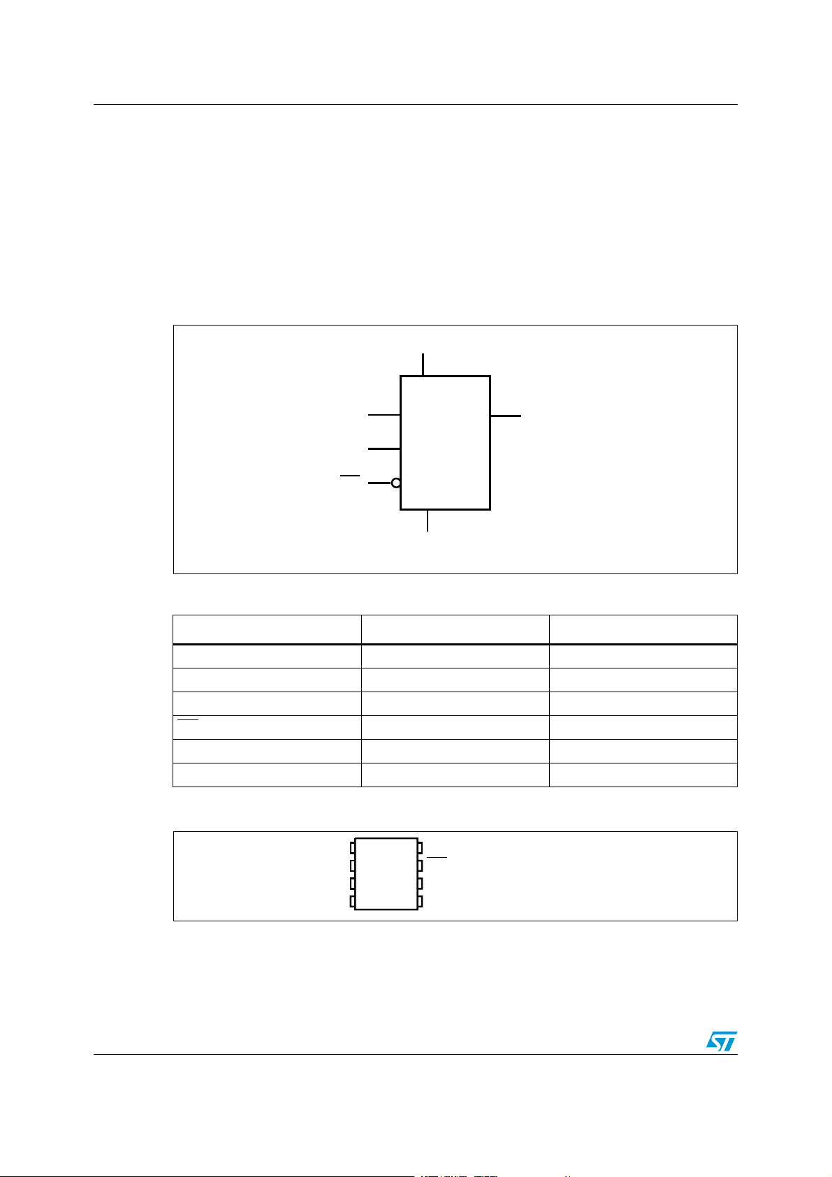
Figure 1. Logic diagram . . . . . . . . . . . . . . . . . . . . . . . . . . . . . . . . . . . . . . . . . . . . . . . . . . . . . . . . . . . . 6
Figure 2. SO8 connections . . . . . . . . . . . . . . . . . . . . . . . . . . . . . . . . . . . . . . . . . . . . . . . . . . . . . . . . . 6
Figure 3. Device select code . . . . . . . . . . . . . . . . . . . . . . . . . . . . . . . . . . . . . . . . . . . . . . . . . . . . . . . . 7
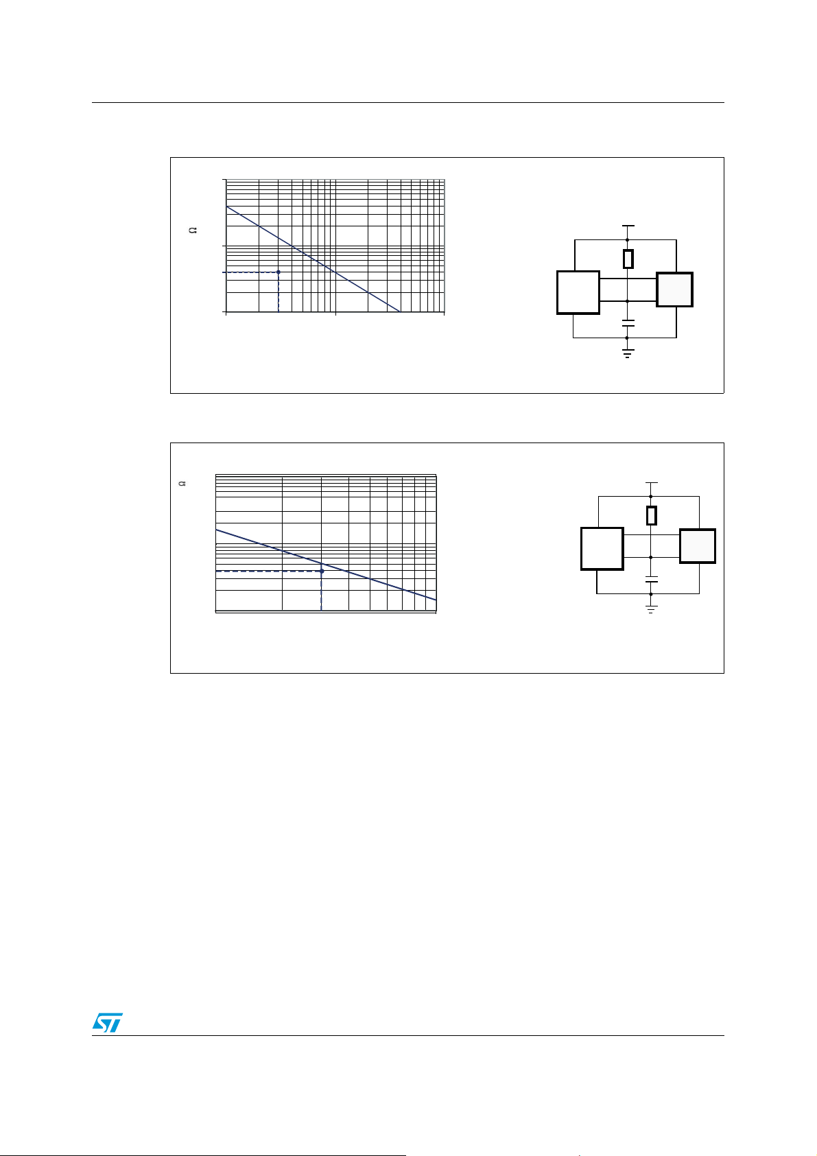
Figure 4. Maximum R
bus at maximum frequency f
Figure 5. Maximum R
bus at maximum frequency f
Figure 6. I
2
C bus protocol . . . . . . . . . . . . . . . . . . . . . . . . . . . . . . . . . . . . . . . . . . . . . . . . . . . . . . . . . 10
Figure 7. Write mode sequences with WC
Figure 8. Write mode sequences with WC
Figure 9. Write cycle polling flowchart using ACK . . . . . . . . . . . . . . . . . . . . . . . . . . . . . . . . . . . . . . . 17
Figure 10. Read mode sequences . . . . . . . . . . . . . . . . . . . . . . . . . . . . . . . . . . . . . . . . . . . . . . . . . . . . 18
Figure 11. AC measurement I/O waveform . . . . . . . . . . . . . . . . . . . . . . . . . . . . . . . . . . . . . . . . . . . . . 22
Figure 12. AC waveforms . . . . . . . . . . . . . . . . . . . . . . . . . . . . . . . . . . . . . . . . . . . . . . . . . . . . . . . . . . 26
Figure 13. SO8N – 8-lead plastic small outline, 150 mils body width, package outline . . . . . . . . . . . . 27
value versus bus parasitic capacitance (C
bus
value versus bus parasitic capacitance (C
bus
= 400 kHz . . . . . . . . . . . . . . . . . . . . . . . . . . . . . . . . . . . . . . . 9
C
= 1 MHz . . . . . . . . . . . . . . . . . . . . . . . . . . . . . . . . . . . . . . . . 9
C
= 1 (data write inhibited) . . . . . . . . . . . . . . . . . . . . . . . . . 13
= 0 (data write enabled) . . . . . . . . . . . . . . . . . . . . . . . . . 15
) for an I2C
bus
) for an I2C
bus
Doc ID 18204 Rev 4 5/30
Description M24M02-DR
1 Description
The M24M02-DR is an I2C-compatible electrically erasable programmable memory
(EEPROM) device organized as 256 Kb × 8 bits.
The M24M02-DR offers an additional page, named the Identification Page (256 bytes) which
can be written and (later) permanently locked in Read-only mode. This Identification Page
offers flexibility in the application board production line, as it can be used to store unique
identification parameters and/or parameters specific to the production line.
Figure 1. Logic diagram
6
6
##
##
%
%
3#,
3#,
7#
7#
--$2
--$2
3$!
3$!
6
6
33
33
!)
!)
Table 1. Signal names
Signal name Function Direction
E2 Chip Enable Input
SDA Serial Data I/O
SCL Serial Clock Input
WC
V
CC
V
SS
Write Control Input
Supply voltage
Ground
Figure 2. SO8 connections
$5 6
%
33
1. See Section 7: Package mechanical data for package dimensions, and how to identify pin-1.
2. DU = Don’t Use (the pin must be left floating or connected to Vss).
##
7#$5
3#,
3$!6
!)V
6/30 Doc ID 18204 Rev 4
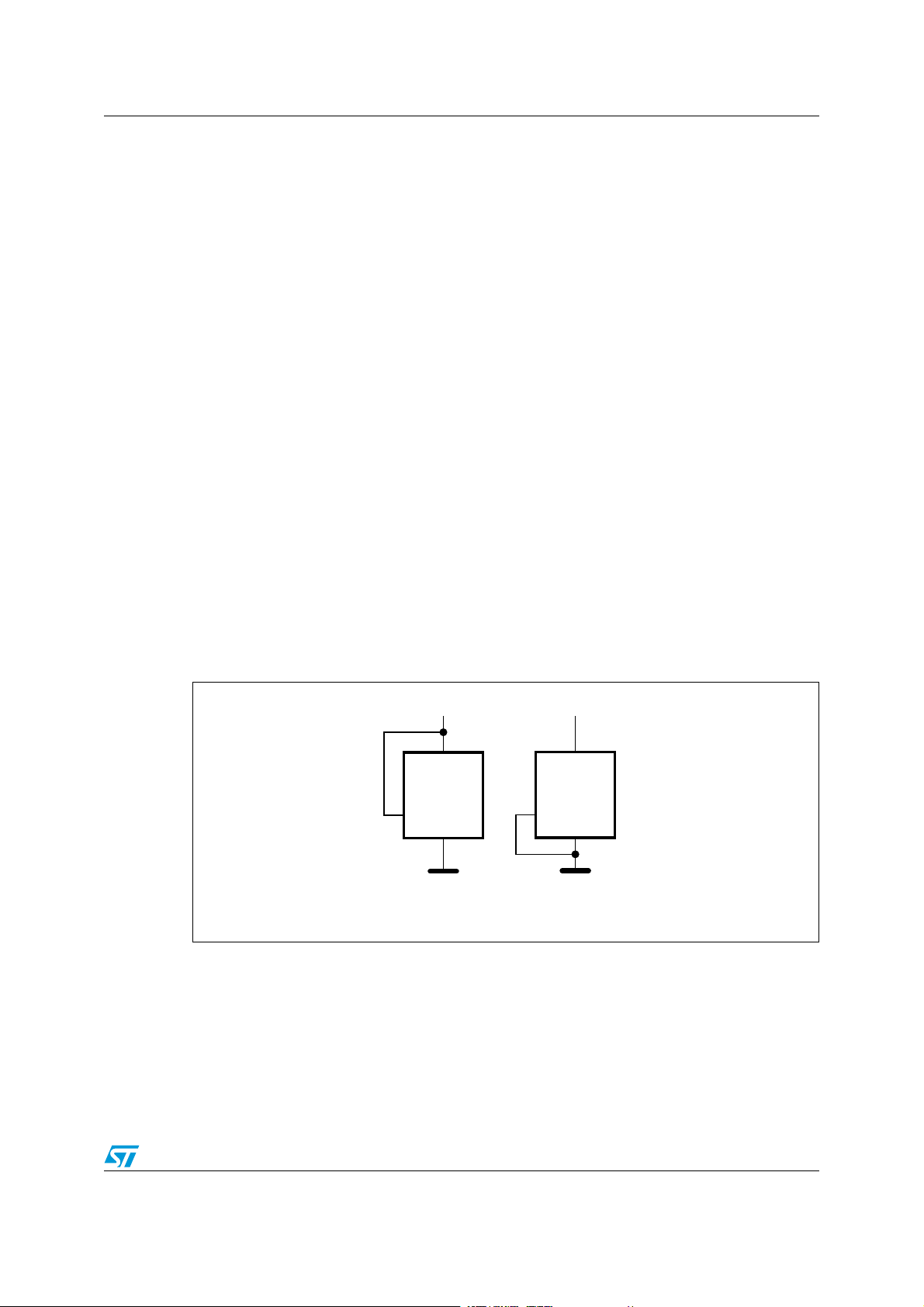
M24M02-DR Signal description
Ai12806
V
CC
M24xxx
V
SS
E
i
V
CC
M24xxx
V
SS
E
i
Ai12806
V
CC
M24xxx
V
SS
E
i
V
CC
M24xxx
V
SS
E
i
2 Signal description
2.1 Serial Clock (SCL)
This input signal is used to strobe all data in and out of the device. In applications where this
signal is used by slave devices to synchronize the bus to a slower clock, the bus master
must have an open drain output, and a pull-up resistor must be connected from Serial Clock
(SCL) to V
most applications, though, this method of synchronization is not employed, and so the pullup resistor is not necessary, provided that the bus master has a push-pull (rather than open
drain) output.
2.2 Serial Data (SDA)
This bidirectional signal is used to transfer data in or out of the device. It is an open drain
output that may be wire-OR’ed with other open drain or open collector signals on the bus. A
pull up resistor must be connected from Serial Data (SDA) to V
the value of the pull-up resistor can be calculated).
. (Figure 5 indicates how the value of the pull-up resistor can be calculated). In
CC
(Figure 5 indicates how
CC
2.3 Chip Enable (E2)
This input signal is used to set the value that is to be looked for on the bit b3 of the 7-bit
device select code. This input must be tied to V
code as shown in Figure 3. When not connected (left floating), this input is read as low (0).
Figure 3. Device select code
or VSS, to establish the device select
CC
Doc ID 18204 Rev 4 7/30

Signal description M24M02-DR
2.4 Write Control (WC)
This input signal is useful for protecting the entire contents of the memory from inadvertent
write operations. Write operations are disabled to the entire memory array when Write
Control (WC
Write operations are allowed.
) is driven high. When unconnected, the signal is internally read as VIL, and
When Write Control (WC
acknowledged, Data bytes are not acknowledged.
) is driven high, device select and address bytes are
2.5 VSS ground
VSS is the reference for the VCC supply voltage.
2.6 Supply voltage (VCC)
2.6.1 Operating supply voltage V
Prior to selecting the memory and issuing instructions to it, a valid and stable VCC voltage
within the specified [V
secure a stable DC supply voltage, it is recommended to decouple the V
suitable capacitor (usually of the order of 10 nF to 100 nF) close to the V
pins.
This voltage must remain stable and valid until the end of the transmission of the instruction
and, for a write instruction, until the completion of the internal write cycle (t
2.6.2 Power-up conditions
The VCC voltage has to rise continuously from 0 V up to the minimum VCC operating voltage
defined in Ta bl e 7 and the rise time must not vary faster than 1 V/µs.
(min), VCC(max)] range must be applied (see Tab l e 7 ). In order to
CC
CC
line with a
CC
CC/VSS
).
W
package
2.6.3 Device reset
In order to prevent inadvertent write operations during power-up, a power-on-reset (POR)
circuit is included. At power-up, the device does not respond to any instruction until V
reached the internal reset threshold voltage. This threshold is lower than the minimum V
operating voltage defined in Ta bl e 7 ). When VCC passes over the POR threshold, the device
is reset and enters the Standby Power mode. The device must not be accessed until V
reaches a valid and stable V
defined in Ta bl e 7 .
In a similar way, during power-down (continuous decrease in V
below the power-on-reset threshold voltage, the device stops responding to any instruction
sent to it.
voltage within the specified [VCC(min), VCC(max)] range
CC
2.6.4 Power-down conditions
During power-down (continuous decrease in VCC), the device must be in the Standby Power
mode (mode reached after decoding a Stop condition, assuming that is there is no internal
write cycle in progress).
8/30 Doc ID 18204 Rev 4
), as soon as VCC drops
CC
CC
has
CC
CC
M24M02-DR Signal description
AIB
"USLINECAPACITORP&
"USLINEPULLUPRESISTOR
K
)£#BUS
MASTER
-XXX
2
BUS
6
##
#
BUS
3#,
3$!
2
BUS
§
#
BUS
NS
(ERE2
BUS
§#
BUS
NS
K½
P&
4HE2X#TIMECONSTANT
MUSTBEBELOWTHENS
TIMECONSTANTLINEREPRESENTED
ONTHELEFT
BUS
BUS
Figure 4. Maximum R
bus at maximum frequency f
Figure 5. Maximum R
bus at maximum frequency f
2
BU
§
S
#
BU
NS
S
2
BUS
value versus bus parasitic capacitance (C
bus
value versus bus parasitic capacitance (C
bus
§
(ERE
NS
#
BUS
= 400 kHz
C
= 1 MHz
C
4HE2
§#
BUS
MUSTBEBELOWTHENS
TIMECONSTANTLINEREPRESENTED
ONTHELEFT
TIMECONSTANT
BUS
)£#BUS
MASTER
) for an I2C
bus
) for an I2C
bus
6
##
2
3#,
3$!
BUS
-XXX
#
BUS
"USLINEPULLUPRESISTORK
"USLINECAPACITORP&
Doc ID 18204 Rev 4 9/30
-36
 Loading...