

ST M24C64, M24C32 User Manual
M24C64
M24C32
64Kbit and 32Kbit Serial I²C Bus EEPROM
FEATURES SUMMARY
M24C64
M24C32
2
C Serial Interface
M24C64
M24C64-W
M24C64-R
M24C32
M24C32-W
M24C32-R
■ Two-Wire I
Supports 400kHz Protocol
■ Single Supply Voltage:
– 4.5 to 5.5V for M24Cxx
– 2.5 to 5.5V for M24Cxx-W
– 1.8 to 5.5V for M24Cxx-R
■ Write Control Input
■ BYTE and PAGE WRITE (up to 32 Bytes)
■ RANDOM and SEQUENTIAL READ Modes
■ Self-Timed Programming Cycle
■ Automatic Address Incr em ent ing
■ Enhanced ESD/Latch-Up Protection
■ More than 1 Million Erase/Write Cycles
■ More than 40-Year Data Retention
Table 1. Product List
Reference Part Number
Figure 1. Packages
8
1
PDIP8 (BN)
8
1
SO8 (MN)
150 mil width
TSSOP8 (DW)
169 mil width
UFDFPN8 (MB)
2x3mm² (MLP)
1/26January 2005

M24C64, M24C32
TABLE OF CONTENTS
FEATURES SUMMARY . . . . . . . . . . . . . . . . . . . . . . . . . . . . . . . . . . . . . . . . . . . . . . . . . . . . . . . . . . . . . 1
Table 1. Product List . . . . . . . . . . . . . . . . . . . . . . . . . . . . . . . . . . . . . . . . . . . . . . . . . . . . . . . . . . . . 1
Figure 1. Packages. . . . . . . . . . . . . . . . . . . . . . . . . . . . . . . . . . . . . . . . . . . . . . . . . . . . . . . . . . . . . . 1
SUMMARY DESCRIPTION. . . . . . . . . . . . . . . . . . . . . . . . . . . . . . . . . . . . . . . . . . . . . . . . . . . . . . . . . . . 4
Figure 2. Logic Diagram . . . . . . . . . . . . . . . . . . . . . . . . . . . . . . . . . . . . . . . . . . . . . . . . . . . . . . . . . . 4
Table 2. Signal Names . . . . . . . . . . . . . . . . . . . . . . . . . . . . . . . . . . . . . . . . . . . . . . . . . . . . . . . . . . 4
Power On Reset: VCC Lock-Out Write Protect . . . . . . . . . . . . . . . . . . . . . . . . . . . . . . . . . . . . . . . 4
Figure 3. DIP, SO, TSSOP and UFDFPN Connections . . . . . . . . . . . . . . . . . . . . . . . . . . . . . . . . . . 4
SIGNAL DESCRIPTION . . . . . . . . . . . . . . . . . . . . . . . . . . . . . . . . . . . . . . . . . . . . . . . . . . . . . . . . . . . . . 5
Serial Clock (SCL). . . . . . . . . . . . . . . . . . . . . . . . . . . . . . . . . . . . . . . . . . . . . . . . . . . . . . . . . . . . . . . 5
Serial Data (SDA) . . . . . . . . . . . . . . . . . . . . . . . . . . . . . . . . . . . . . . . . . . . . . . . . . . . . . . . . . . . . . . . 5
Chip Enable (E0, E1, E2) . . . . . . . . . . . . . . . . . . . . . . . . . . . . . . . . . . . . . . . . . . . . . . . . . . . . . . . . . 5
Write Control (WC
Figure 4. Maximum R
Figure 5. I
2
Table 3. Device Select Code . . . . . . . . . . . . . . . . . . . . . . . . . . . . . . . . . . . . . . . . . . . . . . . . . . . . . . 6
Table 4. Most Significant Byte . . . . . . . . . . . . . . . . . . . . . . . . . . . . . . . . . . . . . . . . . . . . . . . . . . . . . 6
Table 5. Least Significant Byte . . . . . . . . . . . . . . . . . . . . . . . . . . . . . . . . . . . . . . . . . . . . . . . . . . . . 6
) . . . . . . . . . . . . . . . . . . . . . . . . . . . . . . . . . . . . . . . . . . . . . . . . . . . . . . . . . . . . . . 5
Value versus Bus Capacitance (C
L
) for an I2C Bus . . . . . . . . . . . . . . . . 5
BUS
C Bus Protocol . . . . . . . . . . . . . . . . . . . . . . . . . . . . . . . . . . . . . . . . . . . . . . . . . . . . . . . . 6
MEMORY ORGANIZATION . . . . . . . . . . . . . . . . . . . . . . . . . . . . . . . . . . . . . . . . . . . . . . . . . . . . . . . . . . 7
Figure 6. Block Diagram . . . . . . . . . . . . . . . . . . . . . . . . . . . . . . . . . . . . . . . . . . . . . . . . . . . . . . . . . . 7
DEVICE OPERATION . . . . . . . . . . . . . . . . . . . . . . . . . . . . . . . . . . . . . . . . . . . . . . . . . . . . . . . . . . . . . . . 8
Start Condition. . . . . . . . . . . . . . . . . . . . . . . . . . . . . . . . . . . . . . . . . . . . . . . . . . . . . . . . . . . . . . . . . 8
Stop Condition. . . . . . . . . . . . . . . . . . . . . . . . . . . . . . . . . . . . . . . . . . . . . . . . . . . . . . . . . . . . . . . . . 8
Acknowledge Bit (ACK) . . . . . . . . . . . . . . . . . . . . . . . . . . . . . . . . . . . . . . . . . . . . . . . . . . . . . . . . . 8
Data Input. . . . . . . . . . . . . . . . . . . . . . . . . . . . . . . . . . . . . . . . . . . . . . . . . . . . . . . . . . . . . . . . . . . . . 8
Memory Addressing . . . . . . . . . . . . . . . . . . . . . . . . . . . . . . . . . . . . . . . . . . . . . . . . . . . . . . . . . . . . 8
Table 6. Operating Modes . . . . . . . . . . . . . . . . . . . . . . . . . . . . . . . . . . . . . . . . . . . . . . . . . . . . . . . . 8
Figure 7. Write Mode Sequences with WC
=1 (data write inhibited) . . . . . . . . . . . . . . . . . . . . . . . . . 9
Write Operations . . . . . . . . . . . . . . . . . . . . . . . . . . . . . . . . . . . . . . . . . . . . . . . . . . . . . . . . . . . . . . . 9
Byte Write. . . . . . . . . . . . . . . . . . . . . . . . . . . . . . . . . . . . . . . . . . . . . . . . . . . . . . . . . . . . . . . . . . . . . 9
Page Write . . . . . . . . . . . . . . . . . . . . . . . . . . . . . . . . . . . . . . . . . . . . . . . . . . . . . . . . . . . . . . . . . . . 10
Figure 8. Write Mode Sequences with WC
=0 (data write enabled) . . . . . . . . . . . . . . . . . . . . . . . . 10
Figure 9. Write Cycle Polling Flowchart using ACK . . . . . . . . . . . . . . . . . . . . . . . . . . . . . . . . . . . . 11
Minimizing System Delays by Polling On ACK. . . . . . . . . . . . . . . . . . . . . . . . . . . . . . . . . . . . . . 11
Figure 10.Read Mode Sequences. . . . . . . . . . . . . . . . . . . . . . . . . . . . . . . . . . . . . . . . . . . . . . . . . .12
Read Operations . . . . . . . . . . . . . . . . . . . . . . . . . . . . . . . . . . . . . . . . . . . . . . . . . . . . . . . . . . . . . . 12
Random Address Read . . . . . . . . . . . . . . . . . . . . . . . . . . . . . . . . . . . . . . . . . . . . . . . . . . . . . . . . . 12
Current Address Read . . . . . . . . . . . . . . . . . . . . . . . . . . . . . . . . . . . . . . . . . . . . . . . . . . . . . . . . . 12
Sequential Read. . . . . . . . . . . . . . . . . . . . . . . . . . . . . . . . . . . . . . . . . . . . . . . . . . . . . . . . . . . . . . . 13
2/26

M24C64, M24C32
Acknowledge in Read Mode . . . . . . . . . . . . . . . . . . . . . . . . . . . . . . . . . . . . . . . . . . . . . . . . . . . . .13
INITIAL DELIVERY STATE. . . . . . . . . . . . . . . . . . . . . . . . . . . . . . . . . . . . . . . . . . . . . . . . . . . . . . . . . . 13
MAXIMUM RATING. . . . . . . . . . . . . . . . . . . . . . . . . . . . . . . . . . . . . . . . . . . . . . . . . . . . . . . . . . . . . . . . 14
Table 7. Absolute Maximum Ratings. . . . . . . . . . . . . . . . . . . . . . . . . . . . . . . . . . . . . . . . . . . . . . . 14
DC AND AC PARAMETERS. . . . . . . . . . . . . . . . . . . . . . . . . . . . . . . . . . . . . . . . . . . . . . . . . . . . . . . . . 15
Table 8. Operating Conditions (M24Cxx-6). . . . . . . . . . . . . . . . . . . . . . . . . . . . . . . . . . . . . . . . . . 15
Table 9. Operating Conditions (M24Cxx-W) . . . . . . . . . . . . . . . . . . . . . . . . . . . . . . . . . . . . . . . . . 15
Table 10. Operating Conditions (M24Cxx-R). . . . . . . . . . . . . . . . . . . . . . . . . . . . . . . . . . . . . . . . . . 15
Table 11. AC Measurement Conditions. . . . . . . . . . . . . . . . . . . . . . . . . . . . . . . . . . . . . . . . . . . . . . 16
Figure 11.AC Measurement I/O Waveform . . . . . . . . . . . . . . . . . . . . . . . . . . . . . . . . . . . . . . . . . . . 16
Table 12. Input Parameters . . . . . . . . . . . . . . . . . . . . . . . . . . . . . . . . . . . . . . . . . . . . . . . . . . . . . . . 16
Table 13. DC Characteristics (M24Cxx
Table 14. DC Characteristics (M24Cxx-W6 and M24Cxx-W3) . . . . . . . . . . . . . . . . . . . . . . . . . . . . 17
Table 15. DC Characteristics (M24Cxx-R) . . . . . . . . . . . . . . . . . . . . . . . . . . . . . . . . . . . . . . . . . . . 17
Table 16. AC Characteristics (M24Cxx-6, M24Cxx-W6 and M24Cxx-W3) . . . . . . . . . . . . . . . . . . . 18
Table 17. AC Characteristics (M24Cxx-R). . . . . . . . . . . . . . . . . . . . . . . . . . . . . . . . . . . . . . . . . . . . 18
Figure 12.AC Waveforms . . . . . . . . . . . . . . . . . . . . . . . . . . . . . . . . . . . . . . . . . . . . . . . . . . . . . . . . 19
(1)
, M24Cxx-W6 and M24Cxx-W3). . . . . . . . . . . . . . . . . . . 16
PACKAGE MECHANICAL . . . . . . . . . . . . . . . . . . . . . . . . . . . . . . . . . . . . . . . . . . . . . . . . . . . . . . . . . . 20
Figure 13.PDIP8 – 8 pin Plastic DIP, 0.25mm lead frame, Package Outline . . . . . . . . . . . . . . . . . 20
Table 18. PDIP8 – 8 pin Plastic DIP, 0.25mm lead frame, Package Mechanical Data . . . . . . . . . . 20
Figure 14.SO8 narrow – 8 lead Plastic Small Outline, 150 mils body width, Package Outline . . . . 21
Table 19. SO8 narrow – 8 lead Plastic Small Outline, 150 mils body width,
Package Mechanical Data. . . . . . . . . . . . . . . . . . . . . . . . . . . . . . . . . . . . . . . . . . . . . . . . 21
Figure 15.TSSOP8 – 8 lead Thin Shrink Small Outline, Package Outline . . . . . . . . . . . . . . . . . . . 22
Table 20. TSSOP8 – 8 lead Thin Shrink Small Outline, Package Mechanical Data . . . . . . . . . . . . 22
Figure 16.UFDFPN8 (MLP8) – 8-lead Ultra thin Fine pitch Dual Flat Package No lead 2x3mm. . . 23
Table 21. UFDFPN8 (MLP8) – 8-lead Ultra thin Fine pitch Dual Flat Package No lead 2x3mm,
Package Mechanical Data. . . . . . . . . . . . . . . . . . . . . . . . . . . . . . . . . . . . . . . . . . . . . . . . 23
PART NUMBERING . . . . . . . . . . . . . . . . . . . . . . . . . . . . . . . . . . . . . . . . . . . . . . . . . . . . . . . . . . . . . . . 24
Table 22. Ordering Information Scheme . . . . . . . . . . . . . . . . . . . . . . . . . . . . . . . . . . . . . . . . . . . . . 24
REVISION HISTORY. . . . . . . . . . . . . . . . . . . . . . . . . . . . . . . . . . . . . . . . . . . . . . . . . . . . . . . . . . . . . . . 25
Table 23. Document Revision History . . . . . . . . . . . . . . . . . . . . . . . . . . . . . . . . . . . . . . . . . . . . . . . 25
3/26
M24C64, M24C32
SUMMARY DESCRIPTION
These I2C-compatible electrically erasable programmable memory (EEPROM) devices are organized as 8192 x 8 bits (M24C64) and 4096 x 8 bits
(M24C32).
Table 2. Signal Names
E0, E1, E2 Chip Enable
SDA Serial Data
Figure 2. Logic Diagram
V
CC
3
E0-E2 SDA
SCL
WC
2
I
C uses a two-wire serial interf ace, comprisi ng a
M24C64
M24C32
V
SS
AI01844B
bi-directional data line and a clock line. The devices carry a built-in 4-bit Device Type Identifier code
(1010) in accordance with the I
The device behaves as a slave in the I
2
C bus definition.
2
C protocol,
with all memory operations synchronized by the
serial clock. Read and Write operations are initiated by a Start condition, generated by the bus master. The Start condition is followed by a Device
Select Code and Read/Write
bit (RW) (as described in Table 3.), terminated by an acknowledge bit.
When writing data to the memory , the device inserts an acknowled ge bit during the 9
th
bit time,
following the bus master’s 8-bit transmission.
When data is read by the bus master, the bus
master acknowledge s the rec eipt o f the d ata by te
in the same way. Data transfers are terminated by
a Stop condition after an Ack for Write, and after a
NoAck for Read.
SCL Serial Clock
WC
V
CC
V
SS
Power On Reset: V
Write Control
Supply Voltage
Ground
Lock-Out Write Protect
CC
In order to prevent data corruption and inadvertent
Write operations during Power-up, a Power On
Reset (POR) circuit is included . At Power-up, the
internal reset i s he ld a cti ve unti l V
has reached
CC
the Power On Reset (POR) threshold voltage, and
all operations are disabled – the device will not respond to any command. In the sam e way, when
V
drops from the operat ing voltage, below the
CC
Power On Reset (PO R) threshold voltage, a ll operations are disabl ed and the device will not respond to any command.
A stable and valid V
(as defined in Table 9. and
CC
Table 10.) must be applied before applying any
logic signal.
Figure 3. DI P, SO, TSSOP and UFDFPN Connections
M24C64
M24C32
E0 V
1
2
E2
3
4
SS
Note: See PACKA GE MECHANICAL section for package dimen-
sions, and how to identify pin-1.
8
7
6
5
AI01845C
CC
WCE1
SCL
SDAV
4/26
SIGNAL DESCRIPTION
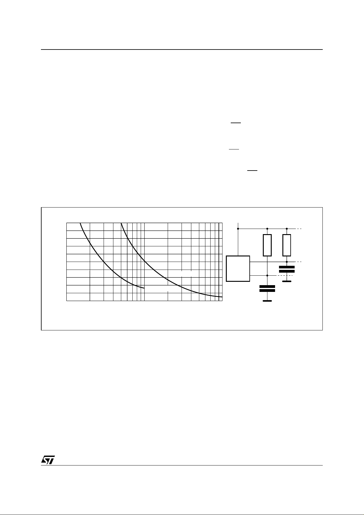
Serial Clock (SCL). This input signal is used to
strobe all data in and out of the device. In applications where this signal is used by slave devices to
synchronize the bus to a slower clock, the bus
master must have an open drain output, and a
pull-up resistor must be connected from Serial
Clock (SCL) to V
value of the pull- up resi stor can be calc ulate d). In
most applications, though, this method of synchronization is not employed, and so the pull-up resistor is not necessary, pro vided that the bus master
has a push-pull (rather than open drain) output.
Serial Data (SDA). This bi-directional signal is
used to transfer data in or out of the device. It is an
open drain output that may be wire-OR’ed with
other open drain or ope n collector signals on the
bus. A pull up resistor must be connected from Se-
. (Figure 4. indicates how the
CC
M24C64, M24C32
rial Data (SDA) to V
the value of the pull-up resistor can be calculated).
Chip Enable (E0, E1, E2). These input signals
are used to set the value that is to be looked for on
the three least significant bits (b3, b2, b1) of the 7bit Device Select Code. These inputs must be tied
to V
or VSS, to establish the Device Select
CC
Code.
Write Control (WC
for protecting the entire content s of the memory
from inadvertent write operations. Write operations are disabled to the entire memory array when
Write Control (WC
nected, the signal is internally read as V
Write operations are allowed.
When Write Contr ol (WC
Select and Address bytes are acknowledged,
Data bytes are not acknowledged.
. (Figure 4. indicates how
CC
). This input signal is useful
) is driven High. When uncon-
, and
IL
) is driven High, Device
Figure 4. Maximum R
20
16
12
8
Maximum RP value (kΩ)
4
0
10
Value versus Bus Capacitance (C
L
fc = 100kHz
fc = 400kHz
100
C
(pF)
BUS
) for an I2C Bus
BUS
MASTER
1000
V
CC
R
SDA
SCL
R
L
C
BUS
L
C
BUS
AI01665
5/26
M24C64, M24C32
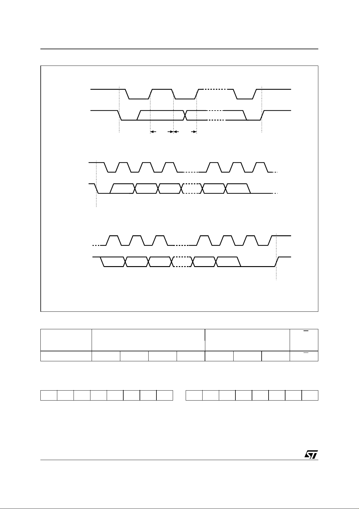
Figure 5. I2C Bus Protocol
SCL
SDA
SCL
SDA
SCL
SDA
START
Condition
START
Condition
1 23 7 89
MSB
1 23 7 89
MSB
SDA
Input
SDA
Change
STOP
Condition
ACK
ACK
STOP
Condition
AI00792B
Table 3. Device Select Code
Device Type Identifier
1
Chip Enable Address
b7 b6 b5 b4 b3 b2 b1 b0
Device Select Code1010E2E1E0RW
Note: 1. The most significant bit, b7, is sent first.
2. E0, E1 and E2 are compared against the respective exte rnal pins on the memory device.
2
RW
Table 4. Most Significant Byte Table 5. Least Significant Byte
b15 b14 b13 b12 b11 b10 b9 b8 b7 b6 b5 b4 b3 b2 b1 b0
6/26
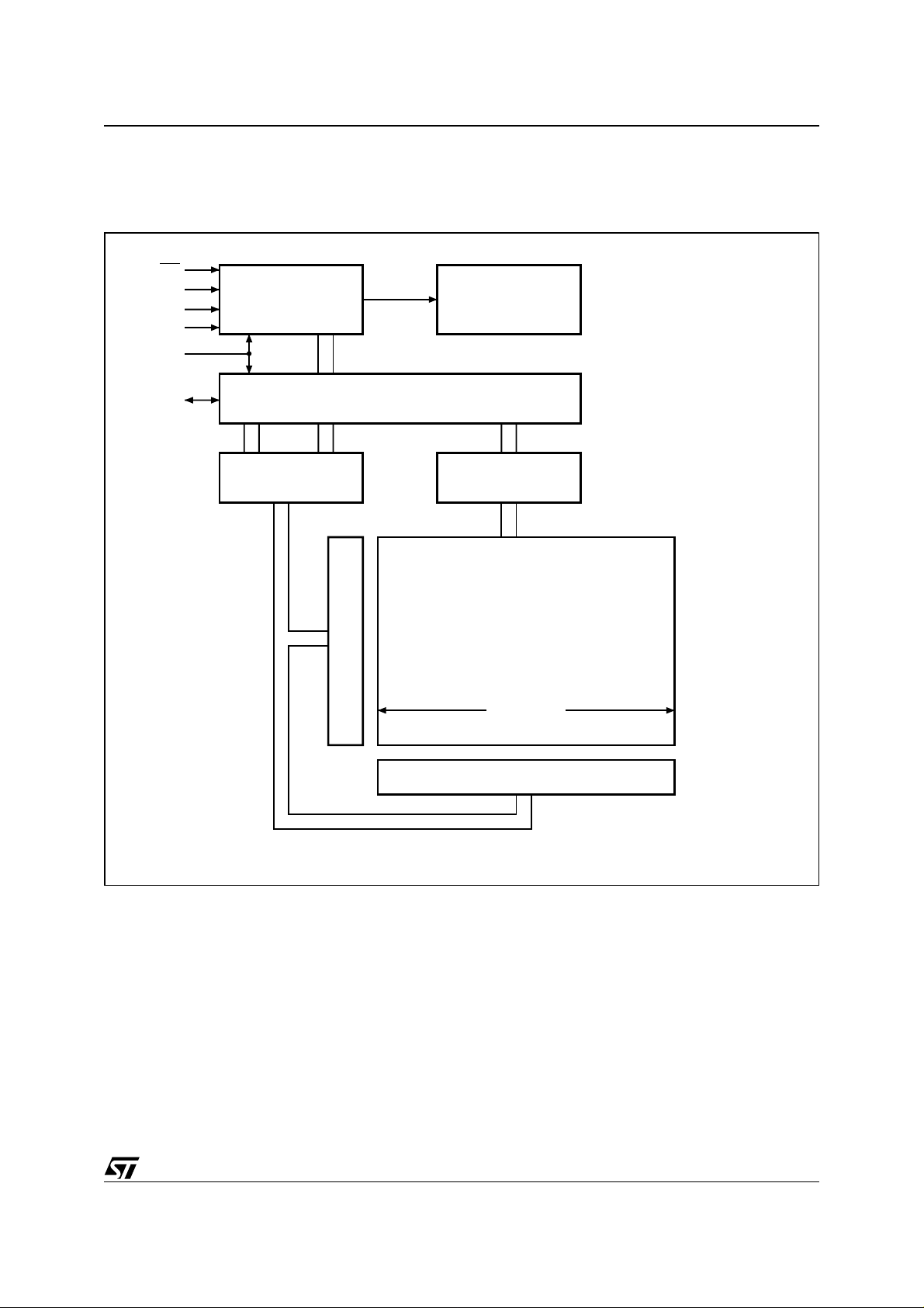
MEMORY ORGANIZATION
The memory is organized as shown in Figure 6..
Figure 6. Block Diagram
WC
E0
E1
E2
SCL
Control Logic
M24C64, M24C32
High Voltage
Generator
SDA
Address Register
and Counter
I/O Shift Register
Data
Register
Y Decoder
1 Page
X Decoder
AI06899
7/26
M24C64, M24C32
DEVICE OPERATION
The device supports the I2C protocol. This is summarized in Figure 5.. Any device that sends d ata
on to the bus is defined to be a transmitter, and
any device that reads the data to be a rec eiver.
The device that controls the data transfer is known
as the bus master, an d th e other a s the s lave device. A data transfer can only be initiated by the
bus master, which will also provide the serial clock
for synchr oniz atio n. Th e M24C xx de vice is alwa ys
a slave in all communication.
Start Condition
Start is identified by a falling edge of Serial Data
(SDA) while Serial Clock (SCL) is stable in the
High state. A Start condition must precede any
data transfer command . The device continuou sly
monitors (except during a Write cycle) Serial Data
(SDA) and Serial Clock (SCL) for a Start condition,
and will not respond unless one is given.
Stop Condition
Stop is identified by a rising edge of Serial Data
(SDA) while Serial Cloc k (S CL) is s tab le a nd d ri ven High. A Stop condition t ermi nate s co mm uni ca tion between the device and the bus master. A
Read command that is follow ed by NoA ck can be
followed by a Sto p condition to force the device
into the Stand-by mode. A S top condition at the
end of a Write command triggers the internal Write
cycle.
Acknowledge Bit (ACK)
The acknowledge bit is used to indicate a successful byte transfer. The bus transmitter, whether it be
bus master or sl ave device, releas es Serial Data
(SDA) after sending ei ght bits of da ta. During the
th
9
clock pulse period, the receiver pulls Serial
Data (SDA) Low to acknowledge the receipt of the
eight data bits.
Data Input
During data input, the device samples Serial Data
(SDA) on the rising edge of Serial Clock (SCL).
For correct device operation, Serial Data (SDA)
must be stable during the rising edge of Serial
Clock (SCL), and the Serial Data (SDA) signal
must change
only
when Serial Cl ock ( SCL ) i s dr iv-
en Low.
Memory Addressing
To start communica tion between the bus master
and the slave device, the b us mas ter m u st ini ti ate
a Start condition. Following this, the bus master
sends the Device Select Code, shown in Table 3.
(on Serial Data (SDA), most significant bit first).
The Device Select Code consists of a 4-bit Device
Type Identifier, and a 3-bit Chip Enable “Address”
(E2, E1, E0). To address the memory array, the 4bit Device Type Identifier is 1010b.
Up to eight memory devices can be connected on
a single I
2
C bus. Each one is gi ven a un ique 3-bit
code on the Chip Enable (E0, E1, E2) inputs.
When the Device Select Code is received, the device only respond s if the Chip Enabl e Address is
the same as the value on the Chip Enable (E0, E1,
E2) inputs.
th
The 8
bit is the Read/Write bit (RW). This bit is
set to 1 for Read and 0 for Write operations.
If a match occurs on the Device Select code, the
corresponding device gives an acknowledgment
on Serial Data (SDA) du ring the 9
th
bit time. If the
device does not match the Devic e Select code, it
deselects itself from the bus, and goes into Standby mode.
Table 6. Operating Modes
Mode RW bit
Current Address Read 1 X 1 START, Device Select, RW
Random Address Read
Sequential Read 1 X ≥ 1 Similar to Current or Random Address Read
Byte Write 0
Page Write 0
Note: 1. X = V
8/26
IH
or V
.
IL
0X
1 X reSTART, Device Select, RW
WC
V
V
1
IL
IL
Bytes Initial Sequence
= 1
1
START, Device Select, RW
1 START, Device Select, RW = 0
≤ 32 START, Device Select, RW = 0
= 0, Address
= 1
Figure 7. Write Mode Sequences with WC=1 (data write inhibited)
WC
ACK ACK ACK NO ACK
BYTE WRITE DEV SEL BYTE ADDR BYTE ADDR DATA IN
M24C64, M24C32
R/W
START
WC
ACK ACK ACK NO ACK
PAGE WRITE DEV SEL BYTE ADDR
R/W
START
WC (cont'd)
NO ACK NO ACK
PAGE WRITE
(cont'd)
DATA IN N
STOP
Write Operations
Following a Start co ndition the bus mas ter sends
a Device Select Code with the Read/Write
(RW
) reset to 0. The device acknowledges this, as
bit
shown in Figure 8., and waits for two address
bytes. The devi ce res ponds to e ach addres s by te
with an acknowledge bit, and then waits for the
data byte.
Writing to the memory may be inhibited if Write
Control (WC
with Write Control (WC
) is driven Hi gh. Any W rite instruction
) driven High (duri ng a pe riod of time from the Start condition until the end of
the two address bytes) will not modify the memory
contents, and the accompanying data bytes are
not
acknowledged, as shown in Figure 7..
Each data byte in the memory ha s a 16-bit (two
byte wide) address. The Most Significant Byte (Ta-
ble 4.) is sent first, foll owed by the Least Signifi-
cant Byte (Table 5.). Bits b15 to b0 form the
address of the byte in memory.
When the bus master gener ates a Stop conditi on
immediately after t he Ac k bi t (i n th e “1 0
th
bit” time
STOP
BYTE ADDR DATA IN 1
DATA IN 2
AI01120C
slot), either at the end of a Byte Write or a Page
Write, the internal W rite c ycle is tri ggered. A Stop
condition at any other time slot does not trigger the
internal Write cycle.
After the Stop condition, the delay t
, and the suc-
W
cessful completion of a Write operation, the device’s internal address counter is incremented
automatically, to point to the next byte address after the last one that was modified.
During the internal Write cycl e, Serial Data (SDA)
is disabled intern ally, a nd the devic e does n ot respond to any requests.
Byte Write
After the Device Select code and the address
bytes, the bus mas ter sends one d ata byte. If the
addressed location is Write-protected, by Write
Control (WC
) being driven High, the device replies
with NoAck, and the location is not modified. If, instead, the addressed location is not Write-protected, the device replies with Ack. The bus master
terminates the transf er by gener ating a St op condition, as shown in Figure 8..
9/26
 Loading...