

16 Kbit, 8 Kbit, 4 Kbit, 2 Kbit and 1 Kbit serial I²C bus EEPROM
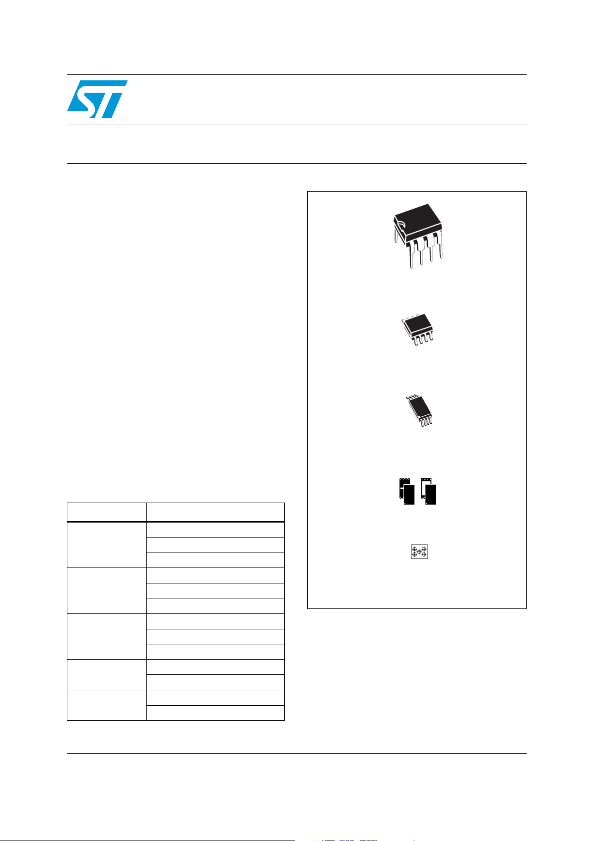
PDIP8 (BN)
SO8 (MN)
150 mils width
TSSOP8 (DW)
169 mils width
UFDFPN8 (MB, MC)
2 × 3 mm (MLP)
WLCSP (CS)
(1)
Thin WLCSP (CT)
(2)
Features
■ Supports both the 100 kHz I
and the 400 kHz I
■ Single supply voltage:
– 2.5 V to 5.5 V for M24Cxx-W
– 1.8 V to 5.5 V for M24Cxx
– 1.7 V to 5.5 V for M24Cxx-F
■ Write Control input
■ Byte and Page Write (up to 16 bytes)
■ Random and Sequential Read modes
■ Self-timed programming cycle
■ Automatic address incrementing
■ Enhanced ESD/latch-up protection
■ More than 1 million write cycles
■ More than 40-year data retention
■ Packages:
– SO8, TSSOP8, UFDFPN8: ECOPACK2
(RoHS-compliant and Halogen-free)
– PDIP8: ECOPACK1
Table 1. Device summary
Reference Part number
M24C16-x
M24C08-x
M24C04-x
M24C02-x
M24C01-x
2
C Fast-mode
®
(RoHS-compliant)
M24C04-x M24C02-x M24C01-x
2
C Standard-mode
M24C16-W
M24C16-R
M24C16-F
M24C08-W
M24C08-R
M24C08-F
M24C04-W
M24C04-R
M24C04-F
M24C02-W
M24C02-R
M24C01-W
M24C01-R
M24C16-x M24C08-x
®
1. Only M24C08-F and M24C16-F devices are offered in
the WLCSP package.
2. Only M24C08-F devices are offered in the Thin
WLCSP package.
April 2011 Doc ID 5067 Rev 17 1/38
www.st.com
1

Contents M24C16, M24C08, M24C04, M24C02, M24C01
Contents
1 Description . . . . . . . . . . . . . . . . . . . . . . . . . . . . . . . . . . . . . . . . . . . . . . . . . 6
2 Signal description . . . . . . . . . . . . . . . . . . . . . . . . . . . . . . . . . . . . . . . . . . . 8
2.1 Serial Clock (SCL) . . . . . . . . . . . . . . . . . . . . . . . . . . . . . . . . . . . . . . . . . . . 8
2.2 Serial Data (SDA) . . . . . . . . . . . . . . . . . . . . . . . . . . . . . . . . . . . . . . . . . . . . 8
2.3 Chip Enable (E0, E1, E2) . . . . . . . . . . . . . . . . . . . . . . . . . . . . . . . . . . . . . . 8
2.3.1 Write Control (WC) . . . . . . . . . . . . . . . . . . . . . . . . . . . . . . . . . . . . . . . . . 8
2.4 Supply voltage (VCC) . . . . . . . . . . . . . . . . . . . . . . . . . . . . . . . . . . . . . . . . . 9
2.4.1 Operating supply voltage V
CC . . . . . . . . . . . . . . . . . . . . . . . . . . . . . . . . . . . . . . . . . . 9
2.4.2 Power-up conditions . . . . . . . . . . . . . . . . . . . . . . . . . . . . . . . . . . . . . . . . 9
2.4.3 Device reset . . . . . . . . . . . . . . . . . . . . . . . . . . . . . . . . . . . . . . . . . . . . . . . 9
2.4.4 Power-down conditions . . . . . . . . . . . . . . . . . . . . . . . . . . . . . . . . . . . . . . 9
3 Device operation . . . . . . . . . . . . . . . . . . . . . . . . . . . . . . . . . . . . . . . . . . . 11
3.1 Start condition . . . . . . . . . . . . . . . . . . . . . . . . . . . . . . . . . . . . . . . . . . . . . 11
3.2 Stop condition . . . . . . . . . . . . . . . . . . . . . . . . . . . . . . . . . . . . . . . . . . . . . 11
3.3 Acknowledge bit (ACK) . . . . . . . . . . . . . . . . . . . . . . . . . . . . . . . . . . . . . . . 11
3.4 Data input . . . . . . . . . . . . . . . . . . . . . . . . . . . . . . . . . . . . . . . . . . . . . . . . . 11
3.5 Memory addressing . . . . . . . . . . . . . . . . . . . . . . . . . . . . . . . . . . . . . . . . . 12
3.6 Write operations . . . . . . . . . . . . . . . . . . . . . . . . . . . . . . . . . . . . . . . . . . . . 13
3.6.1 Byte Write . . . . . . . . . . . . . . . . . . . . . . . . . . . . . . . . . . . . . . . . . . . . . . . 14
3.6.2 Page Write . . . . . . . . . . . . . . . . . . . . . . . . . . . . . . . . . . . . . . . . . . . . . . . 14
3.6.3 Minimizing system delays by polling on ACK . . . . . . . . . . . . . . . . . . . . . 16
3.7 Read operations . . . . . . . . . . . . . . . . . . . . . . . . . . . . . . . . . . . . . . . . . . . . 17
3.7.1 Random Address Read . . . . . . . . . . . . . . . . . . . . . . . . . . . . . . . . . . . . . 17
3.7.2 Current Address Read . . . . . . . . . . . . . . . . . . . . . . . . . . . . . . . . . . . . . . 18
3.7.3 Sequential Read . . . . . . . . . . . . . . . . . . . . . . . . . . . . . . . . . . . . . . . . . . 18
3.7.4 Acknowledge in Read mode . . . . . . . . . . . . . . . . . . . . . . . . . . . . . . . . . 18
4 Initial delivery state . . . . . . . . . . . . . . . . . . . . . . . . . . . . . . . . . . . . . . . . . 19
5 Maximum rating . . . . . . . . . . . . . . . . . . . . . . . . . . . . . . . . . . . . . . . . . . . . 19
6 DC and AC parameters . . . . . . . . . . . . . . . . . . . . . . . . . . . . . . . . . . . . . . 20
2/38 Doc ID 5067 Rev 17

M24C16, M24C08, M24C04, M24C02, M24C01 Contents
7 Package mechanical data . . . . . . . . . . . . . . . . . . . . . . . . . . . . . . . . . . . . 27
8 Part numbering . . . . . . . . . . . . . . . . . . . . . . . . . . . . . . . . . . . . . . . . . . . . 33
9 Revision history . . . . . . . . . . . . . . . . . . . . . . . . . . . . . . . . . . . . . . . . . . . 34
Doc ID 5067 Rev 17 3/38

List of tables M24C16, M24C08, M24C04, M24C02, M24C01
List of tables
Table 1. Device summary . . . . . . . . . . . . . . . . . . . . . . . . . . . . . . . . . . . . . . . . . . . . . . . . . . . . . . . . . . 1
Table 2. Signal names . . . . . . . . . . . . . . . . . . . . . . . . . . . . . . . . . . . . . . . . . . . . . . . . . . . . . . . . . . . . 6
Table 3. Device select code . . . . . . . . . . . . . . . . . . . . . . . . . . . . . . . . . . . . . . . . . . . . . . . . . . . . . . . 10
Table 4. Operating modes . . . . . . . . . . . . . . . . . . . . . . . . . . . . . . . . . . . . . . . . . . . . . . . . . . . . . . . . 12
Table 5. Absolute maximum ratings . . . . . . . . . . . . . . . . . . . . . . . . . . . . . . . . . . . . . . . . . . . . . . . . . 19
Table 6. Operating conditions (M24Cxx-W) . . . . . . . . . . . . . . . . . . . . . . . . . . . . . . . . . . . . . . . . . . . 20
Table 7. Operating conditions (M24Cxx-R) . . . . . . . . . . . . . . . . . . . . . . . . . . . . . . . . . . . . . . . . . . . 20
Table 8. Operating conditions (M24Cxx-F) . . . . . . . . . . . . . . . . . . . . . . . . . . . . . . . . . . . . . . . . . . . . 20
Table 9. DC characteristics (M24Cxx-W, device grade 6) . . . . . . . . . . . . . . . . . . . . . . . . . . . . . . . . 21
Table 10. DC characteristics (M24Cxx-W, device grade 3) . . . . . . . . . . . . . . . . . . . . . . . . . . . . . . . . 21
Table 11. DC characteristics (M24Cxx-R) . . . . . . . . . . . . . . . . . . . . . . . . . . . . . . . . . . . . . . . . . . . . . 22
Table 12. DC characteristics (M24Cxx-F) . . . . . . . . . . . . . . . . . . . . . . . . . . . . . . . . . . . . . . . . . . . . . . 23
Table 13. AC measurement conditions. . . . . . . . . . . . . . . . . . . . . . . . . . . . . . . . . . . . . . . . . . . . . . . . 23
Table 14. Input parameters. . . . . . . . . . . . . . . . . . . . . . . . . . . . . . . . . . . . . . . . . . . . . . . . . . . . . . . . . 23
Table 15. AC characteristics at 400 kHz (I
M24Cxx-F) . . . . . . . . . . . . . . . . . . . . . . . . . . . . . . . . . . . . . . . . . . . . . . . . . . . . . . . . . . . . . 24
Table 16. AC characteristics at 100 kHz (I
M24Cxx-R, M24Cxx-F) . . . . . . . . . . . . . . . . . . . . . . . . . . . . . . . . . . . . . . . . . . . . . . . . . . . . 25
Table 17. M24C08: WLCSP (0.5 mm height) 0.4 mm pitch, 5 bumps, package data . . . . . . . . . . . . 27
Table 18. M24C08: Thin WLCSP (0.3 mm height), 0.4 mm pitch, 5 bumps, package data . . . . . . . . 28
Table 19. M24C16: WLCSP (0.5 mm height) 0.4 mm pitch, 5 bumps, package data . . . . . . . . . . . . 28
Table 20. SO8 narrow – 8 lead plastic small outline, 150 mils body width,
package mechanical data . . . . . . . . . . . . . . . . . . . . . . . . . . . . . . . . . . . . . . . . . . . . . . . . . . 29
Table 21. UFDFPN8 (MLP8) 8-lead ultra thin fine pitch dual flat package no lead
2 x 3 mm, data . . . . . . . . . . . . . . . . . . . . . . . . . . . . . . . . . . . . . . . . . . . . . . . . . . . . . . . . . . 30
Table 22. TSSOP8 – 8 lead thin shrink small outline, package mechanical data. . . . . . . . . . . . . . . . 31
Table 23. PDIP8 – 8 pin plastic DIP, 0.25 mm lead frame, package mechanical data. . . . . . . . . . . . 32
Table 24. Ordering information scheme . . . . . . . . . . . . . . . . . . . . . . . . . . . . . . . . . . . . . . . . . . . . . . . 33
Table 25. Document revision history . . . . . . . . . . . . . . . . . . . . . . . . . . . . . . . . . . . . . . . . . . . . . . . . . 34
2
C Fast-mode) (M24Cxx-W, M24Cxx-R,
2
C Standard-mode) (M24Cxx-W,
4/38 Doc ID 5067 Rev 17

M24C16, M24C08, M24C04, M24C02, M24C01 List of figures
List of figures
Figure 1. Logic diagram . . . . . . . . . . . . . . . . . . . . . . . . . . . . . . . . . . . . . . . . . . . . . . . . . . . . . . . . . . . . 6
Figure 2. 8-pin package connections (top view) . . . . . . . . . . . . . . . . . . . . . . . . . . . . . . . . . . . . . . . . . 7
Figure 3. WLCSP and thin WLCSP connections
(top view, marking side, with balls on the underside) . . . . . . . . . . . . . . . . . . . . . . . . . . . . . 7
Figure 4. Device select code . . . . . . . . . . . . . . . . . . . . . . . . . . . . . . . . . . . . . . . . . . . . . . . . . . . . . . . . 8
Figure 5. Maximum R
Figure 6. I²C bus protocol . . . . . . . . . . . . . . . . . . . . . . . . . . . . . . . . . . . . . . . . . . . . . . . . . . . . . . . . . 10
Figure 7. Write mode sequences with WC
Figure 8. Write mode sequences with WC
Figure 9. Write cycle polling flowchart using ACK . . . . . . . . . . . . . . . . . . . . . . . . . . . . . . . . . . . . . . . 16
Figure 10. Read mode sequences . . . . . . . . . . . . . . . . . . . . . . . . . . . . . . . . . . . . . . . . . . . . . . . . . . . . 17
Figure 11. AC measurement I/O waveform . . . . . . . . . . . . . . . . . . . . . . . . . . . . . . . . . . . . . . . . . . . . . 23
Figure 12. AC waveforms . . . . . . . . . . . . . . . . . . . . . . . . . . . . . . . . . . . . . . . . . . . . . . . . . . . . . . . . . . 26
Figure 13. WLCSP (0.5 mm) and Thin WLCSP (0.3 mm) 0.4 mm pitch 5 bumps,
package outline . . . . . . . . . . . . . . . . . . . . . . . . . . . . . . . . . . . . . . . . . . . . . . . . . . . . . . . . . 27
Figure 14. SO8 narrow – 8 lead plastic small outline, 150 mils body width, package outline . . . . . . . 29
Figure 15. UFDFPN8 (MLP8) 8-lead ultra thin fine pitch dual flat package no lead
2 x 3 mm, outline . . . . . . . . . . . . . . . . . . . . . . . . . . . . . . . . . . . . . . . . . . . . . . . . . . . . . . . . 30
Figure 16. TSSOP8 – 8 lead thin shrink small outline, package outline . . . . . . . . . . . . . . . . . . . . . . . 31
Figure 17. PDIP8 – 8 pin plastic DIP, 0.25 mm lead frame, package outline . . . . . . . . . . . . . . . . . . . 32
value versus bus parasitic capacitance (C) for an I²C bus . . . . . . . . . . . . . . 9
P
= 1 (data write inhibited) . . . . . . . . . . . . . . . . . . . . . . . . . 13
= 0 (data write enabled) . . . . . . . . . . . . . . . . . . . . . . . . . 15
Doc ID 5067 Rev 17 5/38
Description M24C16, M24C08, M24C04, M24C02, M24C01
AI02033
3
E0-E2 SDA
V
CC
M24Cxx
WC
SCL
V
SS
1 Description
These I²C-compatible electrically erasable programmable memory (EEPROM) devices are
organized as 2048/1024/512/256/128
M24C01).
Figure 1. Logic diagram
x 8 (M24C16, M24C08, M24C04, M24C02 and
I²C uses a two-wire serial interface, comprising a bidirectional data line and a clock line. The
devices carry a built-in 4-bit Device Type Identifier code (1010) in accordance with the I²C
bus definition.
The device behaves as a slave in the I²C protocol, with all memory operations synchronized
by the serial clock. Read and Write operations are initiated by a Start condition, generated
by the bus master. The Start condition is followed by a device select code and Read/
bit (R
W) (as described in Ta bl e 3), terminated by an acknowledge bit.
Write
When writing data to the memory, the device inserts an acknowledge bit during the 9th bit
time, following the bus master’s 8-bit transmission. When data is read by the bus master, the
bus master acknowledges the receipt of the data byte in the same way. Data transfers are
terminated by a Stop condition after an Ack for Write, and after a NoAck for Read.
Table 2. Signal names
Signal name Function Direction
E0, E1, E2 Chip Enable Input
SDA Serial Data Input/output
SCL Serial Clock Input
WC
V
CC
V
SS
Write Control Input
Supply voltage
Ground
6/38 Doc ID 5067 Rev 17
M24C16, M24C08, M24C04, M24C02, M24C01 Description
SDAV
SS
SCL
WC
V
CC
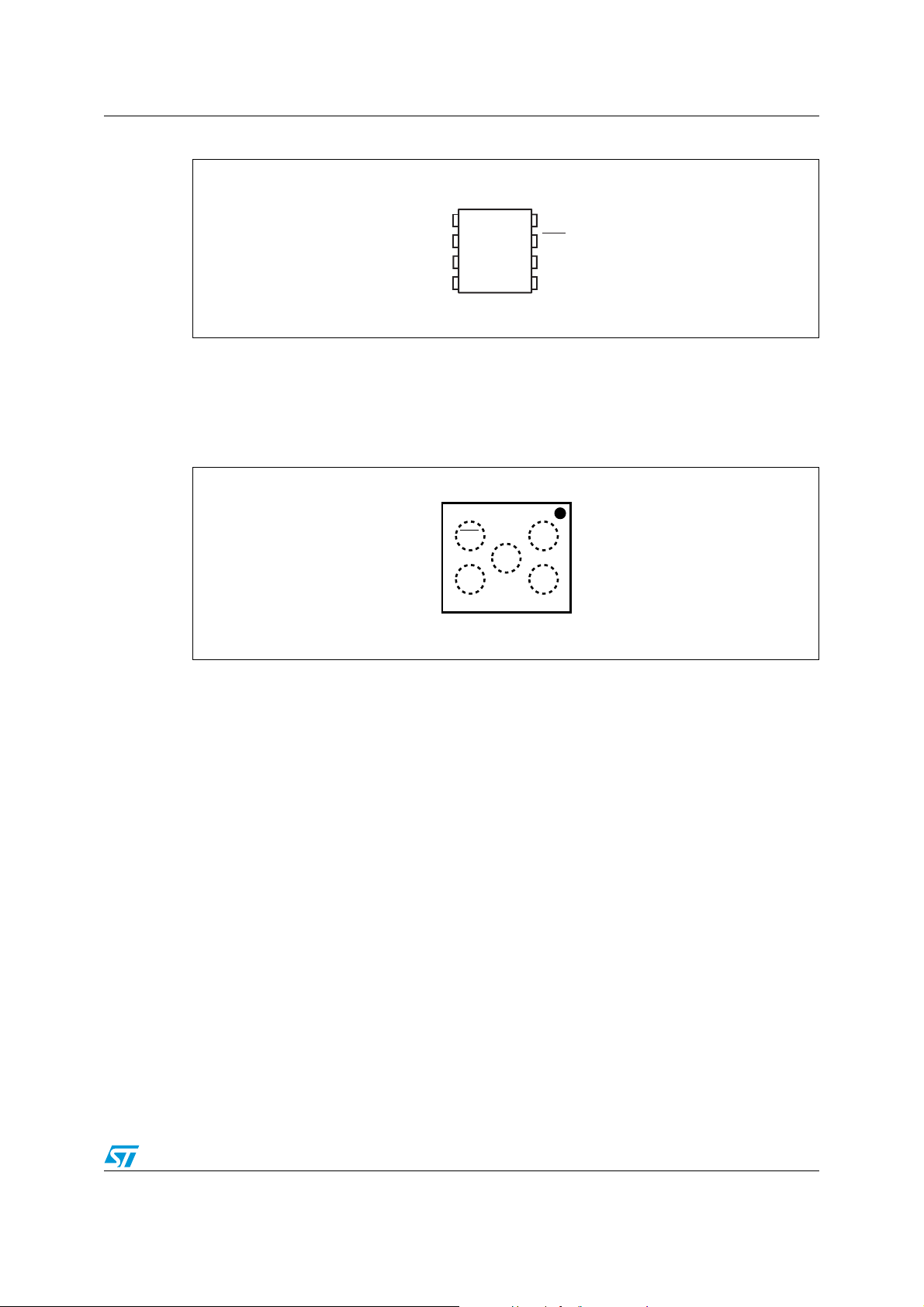
AI02034F
M24Cxx
1
2
3
4
8
7
6
5
16Kb / 8Kb / 4Kb / 2Kb / 1Kb
NC / NC / NC / E0 / E0
NC / NC / E1 / E1 / E1
NC / E2 / E2 / E2 / E2
V
CC
WC
SDA
SCL
V
SS
ai14908
Figure 2. 8-pin package connections (top view)
1. NC = Not connected
2. See Section 7: Package mechanical data for package dimensions, and how to identify pin-1.
3. The Ei inputs are not decoded, and are therefore decoded as “0” (See Section 2.3: Chip Enable (E0, E1,
E2) for more information).
Figure 3. WLCSP and thin WLCSP connections
(top view, marking side, with balls on the underside)
1. For devices of less than 16Kb (see Figure 2: 8-pin package connections (top view)), the Ei inputs are not
connected to a ball, therefore the Ei input is decoded as "0" (see also Section 2.3: Chip Enable (E0, E1,
E2))
Caution: EEPROM dice delivered in wafer form or in WLCSP package by STMicroelectronics must
never be exposed to ultra violet (UV) light, since EEPROM cells loose their charge (and so
their binary value) when exposed to UV light.
Doc ID 5067 Rev 17 7/38
Signal description M24C16, M24C08, M24C04, M24C02, M24C01
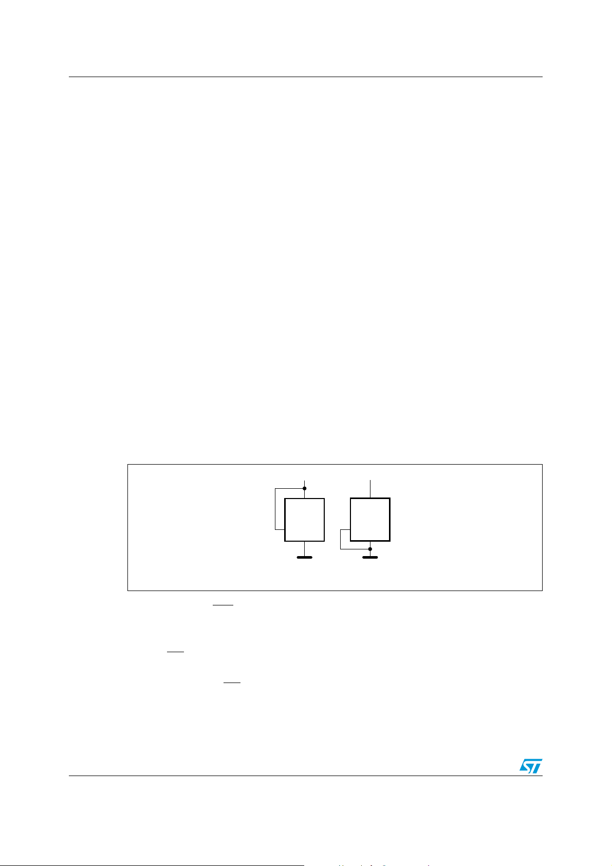
Ai11650
V
CC
M24Cxx
V
SS
E
i
V
CC
M24Cxx
V
SS
E
i
2 Signal description
2.1 Serial Clock (SCL)
This input signal is used to strobe all data in and out of the device. In applications where this
signal is used by slave devices to synchronize the bus to a slower clock, the bus master
must have an open drain output, and a pull-up resistor can be connected from Serial Clock
(SCL) to V
most applications, though, this method of synchronization is not employed, and so the pullup resistor is not necessary, provided that the bus master has a push-pull (rather than open
drain) output.
2.2 Serial Data (SDA)
This bidirectional signal is used to transfer data in or out of the device. It is an open drain
output that may be wire-ORed with other open drain or open collector signals on the bus. A
pull up resistor must be connected from Serial Data (SDA) to V
the value of the pull-up resistor can be calculated).
. (Figure 5 indicates how the value of the pull-up resistor can be calculated). In
CC
. (Figure 5 indicates how
CC
2.3 Chip Enable (E0, E1, E2)
These input signals are used to set the value that is to be looked for on the least significant
bits of the 7-bit device select code. These inputs must be tied to V
device select code as shown in
read as low (0).
Figure 4. Device select code
2.3.1 Write Control (WC)
This input signal is useful for protecting the entire contents of the memory from inadvertent
write operations. Write operations are disabled to the entire memory array when Write
Control (
Write operations are allowed.
When Write Control (WC) is driven High, device select and address bytes are
acknowledged, data bytes are not acknowledged.
WC) is driven High. When unconnected, the signal is internally read as VIL, and
or VSS, to establish the
CC
Figure 4. When not connected (left floating), Ei inputs are
8/38 Doc ID 5067 Rev 17
M24C16, M24C08, M24C04, M24C02, M24C01 Signal description
1
10
100
10 100 1000
Bus line capacitor (pF)
Bus line pull-up resistor
(k
)
When t
LOW
= 1.3 µs (min value for
f
C
= 400 kHz), the R
bus
× C
bus
time constant m ust be below the
400 ns time constant line
represented on the left.
I²C bus
master
M24xxx
R
bus
V
CC
C
bus
SCL
SDA
ai14796b
R
bus
× C
bus
= 400 ns
Here R
bus
× C
bus
= 120 ns
4 kΩ
30 pF
2.4 Supply voltage (VCC)
2.4.1 Operating supply voltage V
Prior to selecting the memory and issuing instructions to it, a valid and stable VCC voltage
within the specified [V
(min), VCC(max)] range must be applied (see Tab l e 6, Ta bl e 7 and
CC
Ta bl e 8). In order to secure a stable DC supply voltage, it is recommended to decouple the
VCC line with a suitable capacitor (usually of the order of 10 nF to 100 nF) close to the
V
CC/VSS
package pins.
This voltage must remain stable and valid until the end of the transmission of the instruction
and, for a Write instruction, until the completion of the internal write cycle (t
2.4.2 Power-up conditions
The VCC voltage has to rise continuously from 0 V up to the minimum VCC operating voltage
defined in
Ta bl e 6, Ta bl e 7 and Ta bl e 8 and the rise time must not vary faster than 1 V/µs.
2.4.3 Device reset
In order to prevent inadvertent write operations during power-up, a power-on-reset (POR)
circuit is included. At power-up (continuous rise of V
instruction until V
than the minimum V
VCC passes over the POR threshold, the device is reset and enters the Standby Power
mode. The device, however, must not be accessed until V
voltage within the specified [V
In a similar way, during power-down (continuous decrease in VCC), as soon as VCC drops
below the power-on-reset threshold voltage, the device stops responding to any instruction
sent to it.
reaches the power-on-reset threshold voltage (this threshold is lower
CC
operating voltage defined in Ta bl e 6, Ta bl e 7 and Ta bl e 8). When
CC
(min), VCC(max)] range.
CC
CC
).
W
), the device does not respond to any
CC
reaches a valid and stable VCC
CC
2.4.4 Power-down conditions
During power-down (continuous decrease in VCC), the device must be in the Standby Power
mode (mode reached after decoding a Stop condition, assuming that there is no internal
write cycle in progress).
Figure 5. Maximum RP value versus bus parasitic capacitance (C) for an I²C bus
Doc ID 5067 Rev 17 9/38
Signal description M24C16, M24C08, M24C04, M24C02, M24C01
SCL
SDA
SCL
SDA
SDA
Start
condition
SDA
Input
SDA
Change
AI00792c
Stop
condition
1 23 7 89
MSB
ACK
Start
condition
SCL
1 23 7 89
MSB ACK
Stop
condition
Figure 6. I²C bus protocol
Table 3. Device select code
Device type identifier
b7 b6 b5 b4 b3 b2 b1 b0
M24C01 select code 1 0 1 0 E2 E1 E0 RW
M24C02 select code 1 0 1 0 E2 E1 E0 RW
M24C04 select code 1 0 1 0 E2 E1 A8 RW
M24C08 select code 1 0 1 0 E2 A9 A8 RW
M24C16 select code 1 0 1 0 A10 A9 A8 RW
1. The most significant bit, b7, is sent first.
2. E0, E1 and E2 are compared against the respective external pins on the memory device.
3. A10, A9 and A8 represent most significant bits of the address.
10/38 Doc ID 5067 Rev 17
(1)
Chip Enable
(2),(3)
RW

M24C16, M24C08, M24C04, M24C02, M24C01 Device operation
3 Device operation
The device supports the I²C protocol. This is summarized in Figure 6. Any device that sends
data on to the bus is defined to be a transmitter, and any device that reads the data to be a
receiver. The device that controls the data transfer is known as the bus master, and the
other as the slave device. A data transfer can only be initiated by the bus master, which will
also provide the serial clock for synchronization. The device is always a slave in all
communication.
3.1 Start condition
Start is identified by a falling edge of Serial Data (SDA) while Serial Clock (SCL) is stable in
the High state. A Start condition must precede any data transfer command. The device
continuously monitors (except during a Write cycle) Serial Data (SDA) and Serial Clock
(SCL) for a Start condition.
3.2 Stop condition
Stop is identified by a rising edge of Serial Data (SDA) while Serial Clock (SCL) is stable
and driven High. A Stop condition terminates communication between the device and the
bus master. A Read command that is followed by NoAck can be followed by a Stop condition
to force the device into the Standby mode. A Stop condition at the end of a Write command
triggers the internal Write cycle.
3.3 Acknowledge bit (ACK)
The acknowledge bit is used to indicate a successful byte transfer. The bus transmitter,
whether it be bus master or slave device, releases Serial Data (SDA) after sending eight bits
of data. During the 9
th
acknowledge the receipt of the eight data bits.
3.4 Data input
During data input, the device samples Serial Data (SDA) on the rising edge of Serial Clock
(SCL). For correct device operation, Serial Data (SDA) must be stable during the rising edge
of Serial Clock (SCL), and the Serial Data (SDA) signal must change only when Serial Clock
(SCL) is driven Low.
clock pulse period, the receiver pulls Serial Data (SDA) Low to
Doc ID 5067 Rev 17 11/38
Device operation M24C16, M24C08, M24C04, M24C02, M24C01
3.5 Memory addressing
To start communication between the bus master and the slave device, the bus master must
initiate a Start condition. Following this, the bus master sends the device select code, shown
in
Ta bl e 3 (on Serial Data (SDA), most significant bit first).
The device select code consists of a 4-bit Device Type Identifier, and a 3-bit Chip Enable
“Address” (E2, E1, E0). To address the memory array, the 4-bit Device Type Identifier is
1010b.
Each device is given a unique 3-bit code on the Chip Enable (E0, E1, E2) inputs. When the
device select code is received, the device only responds if the Chip Enable Address is the
same as the value on the Chip Enable (E0, E1, E2) inputs. However, those devices with
larger memory capacities (the M24C16, M24C08 and M24C04) need more address bits. E0
is not available for use on devices that need to use address line A8; E1 is not available for
devices that need to use address line A9, and E2 is not available for devices that need to
use address line A10 (see
up to eight M24C02 (or M24C01), four M24C04, two M24C08 or one M24C16 devices can
be connected to one I²C bus. In each case, and in the hybrid cases, this gives a total
memory capacity of 16
The 8th bit is the Read/Write bit (RW). This bit is set to 1 for Read and 0 for Write operations.
Figure 2 and Ta bl e 3 for details). Using the E0, E1 and E2 inputs,
Kbits, 2 KBytes (except where M24C01 devices are used).
If a match occurs on the device select code, the corresponding device gives an
acknowledgment on Serial Data (SDA) during the 9
th
bit time. If the device does not match
the device select code, it deselects itself from the bus, and goes into Standby mode.
Table 4. Operating modes
Mode RW bit WC
Current Address Read 1 X 1 Start, Device Select, RW
0X
Random Address Read
1 X reStart, Device Select, RW
Sequential Read 1 X ≥ 1
Byte Write 0 V
Page Write 0 V
1. X = V
IH
or V
.
IL
(1)
Bytes Initial sequence
= 1
Start, Device Select, RW
= 0, Address
1
= 1
Similar to Current or Random Address
Read
IL
IL
1 Start, Device Select, RW = 0
≤ 16 Start, Device Select, RW = 0
12/38 Doc ID 5067 Rev 17

M24C16, M24C08, M24C04, M24C02, M24C01 Device operation
Stop
Start
Byte Write Dev select Byte address Data in
WC
Start
Page Write Dev select Byte address Data in 1 Data in 2
WC
Data in 3
AI02803d
Page Write
(cont'd)
WC (cont'd)
Stop
Data in N
ACK ACK NO ACK
R/W
ACK ACK NO ACK NO ACK
R/W
NO ACK NO ACK
Figure 7. Write mode sequences with WC = 1 (data write inhibited)
3.6 Write operations
Following a Start condition the bus master sends a device select code with the Read/Write
bit (R
W) reset to 0. The device acknowledges this, as shown in Figure 8, and waits for an
address byte. The device responds to the address byte with an acknowledge bit, and then
waits for the data byte.
When the bus master generates a Stop condition immediately after a data byte Ack bit (in
the “10
th
bit” time slot), either at the end of a Byte Write or a Page Write, the internal write
cycle is triggered. A Stop condition at any other time slot does not trigger the internal write
cycle.
After the Stop condition, the tw delay, and the successful completion of a Write operation,
the device internal address counter is automatically incremented, to point to the next byte
address after the last one that was modified. During the internal Write cycle,
Serial
Data (SDA) is disabled internally, and the device does not respond to any request.
If the Write Control (WC) input is driven High, the Write instruction is not executed and the
corresponding data bytes are not acknowledged as shown in
Doc ID 5067 Rev 17 13/38
Figure 7.

Device operation M24C16, M24C08, M24C04, M24C02, M24C01
3.6.1 Byte Write
After the device select code and the address byte, the bus master sends one data byte. If
the addressed location is Write-protected, by Write Control (
device replies to the data byte with NoAck, as shown in
WC) being driven High, the
Figure 7, and the location is not
modified. If, instead, the addressed location is not Write-protected, the device replies with
Ack. The bus master terminates the transfer by generating a Stop condition, as shown in
Figure 8.
3.6.2 Page Write
The Page Write mode allows up to 16 bytes to be written in a single Write cycle, provided
that they are all located in the same page in the memory: that is, the most significant
memory address bits are the same. If more bytes are sent than will fit up to the end of the
page, a condition known as ‘roll-over’ occurs. This should be avoided, as data starts to
become overwritten in an implementation dependent way.
The bus master sends from 1 to 16 bytes of data, each of which is acknowledged by the
device if Write Control (
Control (
in
WC) being driven High, the device replies to the data bytes with NoAck, as shown
Figure 7, and the locations are not modified. After each byte is transferred, the internal
byte address counter (the 4 least significant address bits only) is incremented. The transfer
is terminated by the bus master generating a Stop condition.
WC) is Low. If the addressed location is Write-protected, by Write
14/38 Doc ID 5067 Rev 17

M24C16, M24C08, M24C04, M24C02, M24C01 Device operation
Figure 8. Write mode sequences with WC = 0 (data write enabled)
WC
ACK
Byte Write Dev Select Byte address
Start
R/W
ACK ACK
Data in
Stop
WC
ACK ACK ACK ACK
Page Write Dev Select Byte address Data in 1 Data in 2
Start
R/W
WC (cont'd)
ACKACK
Page Write
Data in N
(cont'd)
Stop
Data in 3
AI02804c
Doc ID 5067 Rev 17 15/38

Device operation M24C16, M24C08, M24C04, M24C02, M24C01
Write cycle
in progress
AI01847d
Next
operation is
addressing the
memory
Start condition
Device select
with RW = 0
ACK
Returned
YES
NO
YESNO
ReStart
Stop
Data for the
Write operation
Device select
with RW = 1
Send Address
and Receive ACK
First byte of instruction
with RW = 0 already
decoded by the device
YESNO
Start
condition
Continue the
Write operation
Continue the
Random Read operation
Figure 9. Write cycle polling flowchart using ACK
3.6.3 Minimizing system delays by polling on ACK
16/38 Doc ID 5067 Rev 17
During the internal Write cycle, the device disconnects itself from the bus, and writes a copy
of the data from its internal latches to the memory cells. The maximum Write time (t
shown in
can be used by the bus master.
The sequence, as shown in Figure 9, is:
Ta bl e 15, but the typical time is shorter. To make use of this, a polling sequence
w
) is
● Initial condition: a Write cycle is in progress.
● Step 1: the bus master issues a Start condition followed by a device select code (the
first byte of the new instruction).
● Step 2: if the device is busy with the internal Write cycle, no Ack will be returned and
the bus master goes back to Step 1. If the device has terminated the internal Write
cycle, it responds with an Ack, indicating that the device is ready to receive the second
part of the instruction (the first byte of this instruction having been sent during Step 1).

M24C16, M24C08, M24C04, M24C02, M24C01 Device operation
Figure 10. Read mode sequences
Current
Address
Read
ACK
Dev select Data out
NO ACK
Random
Address
Read
Sequentila
Current
Read
Sequential
Random
Read
Start
R/W
ACK
Dev select * Byte address
Start
R/W
ACK ACK ACK NO ACK
Dev select Data out 1
Start
R/W
ACK ACK
Dev select * Byte address
Start
R/W
ACK NO ACK
Stop
ACK ACK
Dev select * Data out
Start
R/W
ACK ACK
Dev select * Data out 1
Start
R/W
NO ACK
Stop
Data out N
Stop
1. The seven most significant bits of the device select code of a Random Read (in the 1st and 3rd bytes) must
be identical.
3.7 Read operations
Read operations are performed independently of the state of the Write Control (WC) signal.
The device has an internal address counter which is incremented each time a byte is read.
3.7.1 Random Address Read
A dummy Write is first performed to load the address into this address counter (as shown in
Figure 10) but without sending a Stop condition. Then, the bus master sends another Start
condition, and repeats the device select code, with the Read/Write bit (RW) set to 1. The
device acknowledges this, and outputs the contents of the addressed byte. The bus master
must not acknowledge the byte, and terminates the transfer with a Stop condition.
Data out N
Stop
AI01942b
Doc ID 5067 Rev 17 17/38

Device operation M24C16, M24C08, M24C04, M24C02, M24C01
3.7.2 Current Address Read
For the Current Address Read operation, following a Start condition, the bus master only
sends a device select code with the Read/
Write bit (RW) set to 1. The device acknowledges
this, and outputs the byte addressed by the internal address counter. The counter is then
incremented. The bus master terminates the transfer with a Stop condition
, as shown in
Figure 10, without acknowledging the byte.
3.7.3 Sequential Read
This operation can be used after a Current Address Read or a Random Address Read. The
bus master does acknowledge the data byte output, and sends additional clock pulses so
that the device continues to output the next byte in sequence. To terminate the stream of
bytes, the bus master must not acknowledge the last byte, and must generate a Stop
condition, as shown in
Figure 10.
The output data comes from consecutive addresses, with the internal address counter
automatically incremented after each byte output. After the last memory address, the
address counter ‘rolls-over’, and the device continues to output data from memory address
00h.
3.7.4 Acknowledge in Read mode
For all Read commands, the device waits, after each byte read, for an acknowledgment
during the 9
th
bit time. If the bus master does not drive Serial Data (SDA) Low during this
time, the device terminates the data transfer and switches to its Standby mode.
18/38 Doc ID 5067 Rev 17

M24C16, M24C08, M24C04, M24C02, M24C01 Initial delivery state
4 Initial delivery state
The device is delivered with all bits in the memory array set to 1 (each byte contains FFh).
5 Maximum rating
Stressing the device outside the ratings listed in Ta bl e 5 may cause permanent damage to
the device. These are stress ratings only, and operation of the device at these, or any other
conditions outside those indicated in the operating sections of this specification, is not
implied. Exposure to absolute maximum rating conditions for extended periods may affect
device reliability. Refer also to the STMicroelectronics SURE program and other relevant
quality documents.
Table 5. Absolute maximum ratings
Symbol Parameter Min. Max. Unit
Ambient operating temperature –40 130 °C
T
STG
T
LEAD
I
OL
V
V
CC
V
ESD
1. Compliant with JEDEC Std J-STD-020C (for small body, Sn-Pb or Pb assembly), the ST ECOPACK®
7191395 specification, and the European directive on Restrictions on Hazardous Substances (RoHS)
2002/95/EU.
2. T
LEAD
3. AEC-Q100-002 (compliant with JEDEC Std JESD22-A114, C1 = 100 pF, R1 = 1500 Ω, R2 = 500 Ω).
Storage temperature –65 150 °C
Lead temperature during soldering see note
PDIP-specific lead temperature during soldering - 260
DC output current (SDA = 0) - 5 mA
Input or output range –0.50 6.5 V
IO
Supply voltage –0.50 6.5 V
Electrostatic discharge voltage (human body model)
max must not be applied for more than 10 s.
(3)
- 4000 V
(1)
(2)
°C
°C
Doc ID 5067 Rev 17 19/38

DC and AC parameters M24C16, M24C08, M24C04, M24C02, M24C01
6 DC and AC parameters
This section summarizes the operating and measurement conditions, and the DC and AC
characteristics of the device. The parameters in the DC and AC characteristic tables that
follow are derived from tests performed under the measurement conditions summarized in
the relevant tables. Designers should check that the operating conditions in their circuit
match the measurement conditions when relying on the quoted parameters.
Table 6. Operating conditions (M24Cxx-W)
Symbol Parameter Min. Max. Unit
V
CC
Supply voltage 2.5 5.5 V
Ambient operating temperature (device grade 6) –40 85 °C
Ambient operating temperature (device grade 3) –40 125 °C
Table 7. Operating conditions (M24Cxx-R)
Symbol Parameter Min. Max. Unit
V
CC
Supply voltage 1.8 5.5 V
Ambient operating temperature –40 85 °C
Table 8. Operating conditions (M24Cxx-F)
Symbol Parameter Min. Max. Unit
V
CC
Supply voltage 1.7 5.5 V
Ambient operating temperature –20 85 °C
20/38 Doc ID 5067 Rev 17

M24C16, M24C08, M24C04, M24C02, M24C01 DC and AC parameters
Table 9. DC characteristics (M24Cxx-W, device grade 6)
Symbol Parameter
Test conditions (in addition to those in
Tabl e 6 )
Min. Max. Unit
Input leakage current
I
LI
(SCL, SDA, E0, E1,and E2)
I
Output leakage current
LO
I
Supply current
CC
I
Standby supply current
CC1
Input low voltage (SDA,
V
IL
SCL, WC)
Input high voltage (SDA,
V
IH
SCL, WC
V
Output low voltage
OL
1. The device is not selected after a power-up, after a read command (after the Stop condition), or after the
completion of the internal write cycle tW (tW is triggered by the correct decoding of a write command).
Table 10. DC characteristics (M24Cxx-W, device grade 3)
)
Symbol Parameter
V
= VSS or VCC, device in Standby mode - ± 2 µA
IN
SDA in Hi-Z, external voltage applied on
SS
or V
CC
SDA: V
= 5 V, fc = 400 kHz
V
CC
(rise/fall time < 50 ns)
V
= 2.5 V, fc = 400 kHz
CC
(rise/fall time < 50 ns)
(1)
, V
Device not selected
for 2.5 V < V
= VSS or VCC,
IN
≤ 5.5 V
CC
-± 2µA
-2mA
-1mA
-1µA
–0.45 0.3V
0.7V
CCVCC
= 2.1 mA when VCC = 2.5 V or
I
OL
= 3 mA when VCC = 5.5 V
I
OL
Test condition
(in addition to those in Table 6)
-0.4V
Min. Max. Unit
CC
+1 V
V
Input leakage current (SCL,
I
LI
SDA, E0, E1,and E2)
I
Output leakage current
LO
Supply current
I
CC
I
V
1. The device is not selected after a power-up, after a read command (after the Stop condition), or after the
Standby supply current
CC1
Input low voltage (SDA,
V
IL
SCL, WC)
Input high voltage (SDA,
V
IH
SCL, WC)
Output low voltage
OL
completion of the internal write cycle t
V
= VSS or VCC, device in
IN
Standby mode
SDA in Hi-Z, external voltage
applied on SDA: V
V
= 5 V, fC= 400 kHz
CC
SS
or V
(rise/fall time < 50 ns)
V
= 2.5 V, fC = 400 kHz
CC
(rise/fall time < 50 ns)
(1)
CC
CC
, V
= 5 V
(1)
, V
= 2.5 V
IN
IN
Device not selected
, V
or
VCC
Device not selected
, V
or
VCC
CC
= VSS
= VSS
-± 2µA
-± 2µA
-3mA
-3mA
-5µA
-2µA
–0.45 0.3V
0.7V
CCVCC
= 2.1 mA when VCC = 2.5 V or
I
OL
= 3 mA when VCC = 5.5 V
I
OL
(tW is triggered by the correct decoding of a write command).
W
-0.4V
CC
+1 V
V
Doc ID 5067 Rev 17 21/38

DC and AC parameters M24C16, M24C08, M24C04, M24C02, M24C01
Table 11. DC characteristics (M24Cxx-R)
Symbol Parameter
Input leakage current
I
LI
(SCL, SDA, E0, E1,and E2)
I
I
I
CC1
V
V
V
1. The device is not selected after a power-up, after a read command (after the Stop condition), or after the
completion of the internal write cycle tW (tW is triggered by the correct decoding of a write command).
Output leakage current
LO
Supply current
CC
Standby supply current
Input low voltage (SDA,
IL
SCL, WC)
Input high voltage (SDA,
IH
SCL, WC
Output low voltage IOL = 0.7 mA, VCC = 1.8 V - 0.2 V
OL
)
(in addition to those in Tabl e 7 )
Device not selected
Test condition
V
= VSS or VCC, device in
IN
Standby mode
SDA in Hi-Z, external voltage
applied on SDA: V
= 1.8 V, fc= 400 kHz
V
CC
SS
or V
CC
(rise/fall time < 50 ns)
(1)
, V
= VSS
IN
or VCC, VCC = 1.8 V
2.5 V ≤ V
1.8 V ≤ V
CC
< 2.5 V –0.45 0.25 V
CC
Min. Max. Unit
-± 2µA
-± 2µA
-0.8mA
-1µA
–0.45 0.3 V
0.7V
CCVCC
CC
CC
+1 V
V
V
22/38 Doc ID 5067 Rev 17

M24C16, M24C08, M24C04, M24C02, M24C01 DC and AC parameters
AI00825B
0.8V
CC
0.2V
CC
0.7V
CC
0.3V
CC
Input and Output
Timing Reference Levels
Input Levels
Table 12. DC characteristics (M24Cxx-F)
Symbol Parameter
I
LI
I
LO
I
CC
I
CC1
V
IL
V
IH
V
OL
1. The device is not selected after a power-up, after a read command (after the Stop condition), or after the completion of the
internal write cycle tW (tW is triggered by the correct decoding of a write command).
Table 13. AC measurement conditions
Test condition
(in addition to those in Tab l e 8 )
Input leakage current (SCL, SDA,
E0, E1,and E2)
Output leakage current V
Supply current
Standby supply current
Input low voltage (SDA, SCL, WC)
V
= VSS or VCC, device in Standby mode - ± 2 µA
IN
= VSS or V
OUT
= 1.7 V, fc= 400 kHz
V
CC
SDA in Hi-Z - ± 2 µA
CC,
(rise/fall time < 50 ns)
Device not selected
(1)
, V
IN
= VSS or VCC,
VCC = 1.7 V
2.5 V ≤ V
1.7 V ≤ V
CC
< 2.5 V –0.45 0.25 V
CC
Input high voltage (SDA, SCL, WC)0.7V
Min. Max. Unit
-0.8mA
-1µA
–0.45 0.3 V
CCVCC
CC
CC
+1 V
Output low voltage IOL = 0.7 mA, VCC = 1.7 V - 0.2 V
Symbol Parameter Min. Max. Unit
V
V
C
bus
Load capacitance 100 pF
SCL input rise/fall time, SDA input fall time - 50 ns
Input levels 0.2VCC to 0.8V
Input and output timing reference levels 0.3V
Figure 11. AC measurement I/O waveform
Table 14. Input parameters
Symbol Parameter
C
C
Z
Z
WCL
WCH
t
NS
IN
IN
Input capacitance (SDA) - 8 pF
Input capacitance (other pins) - 6 pF
WC input impedance VIN < 0.3 V 15 70 kΩ
WC input impedance VIN > 0.7V
Pulse width ignored (input filter on
SCL and SDA)
(1)
V
V
to 0.7V
CC
CC
CC
Test condition Min. Max. Unit
CC
500 - kΩ
Single glitch - 100 ns
1. Characterized only.
Doc ID 5067 Rev 17 23/38

DC and AC parameters M24C16, M24C08, M24C04, M24C02, M24C01
Table 15. AC characteristics at 400 kHz (I2C Fast-mode) (M24Cxx-W, M24Cxx-R,
M24Cxx-F)
Test conditions specified in either Ta b l e 6 , Ta b l e 7 or Tabl e 8 and Table 13
Symbol Alt. Parameter Min.
f
C
t
CHCL
t
CLCH
t
QL1QL2
t
XH1XH2
t
XL1XL2
t
DXCX
t
CLDXtHD:DAT
t
CLQX
(5)(6)
t
CLQV
t
CHDL
t
DLCL
t
CHDHtSU:STO
t
DHDL
t
W
(2)
f
SCL
t
HIGH
t
LOW
t
F
t
R
t
F
t
SU:DAT
t
DH
t
AA
t
SU:STA
t
HD:STA
t
BUF
t
WR
Clock frequency - 400 kHz
Clock pulse width high 600 - ns
Clock pulse width low 1300 - ns
SDA (out) fall time 20
Input signal rise time
Input signal fall time
Data in set up time 100 - ns
Data in hold time 0 - ns
Data out hold time 100 - ns
Clock low to next data valid (access time) 200 900 ns
Start condition setup time 600 - ns
Start condition hold time 600 - ns
Stop condition set up time 600 - ns
Time between Stop condition and next Start
condition
Write time - 5 ms
(1)
(3)
(4)
(4) (4)
1300 - ns
(1)
Max.
120 ns
(4)
Unit
ns
ns
1. All values are referred to VIL(max) and VIH(min).
2. Characterized only, not tested in production.
3. With CL = 10 pF.
4. There is no min. or max. values for the input signal rise and fall times. It is however recommended by the
I²C specification that the input signal rise and fall times be more than 20 ns and less than 300 ns when
< 400 kHz.
f
C
5. To avoid spurious Start and Stop conditions, a minimum delay is placed between SCL=1 and the falling or
rising edge of SDA.
6. t
is the time (from the falling edge of SCL) required by the SDA bus line to reach either 0.3VCC or
CLQV
0.7V
, assuming that R
CC
bus
× C
time constant is within the values specified in Figure 5.
bus
24/38 Doc ID 5067 Rev 17

M24C16, M24C08, M24C04, M24C02, M24C01 DC and AC parameters
Table 16. AC characteristics at 100 kHz (I2C Standard-mode)
(1)
(M24Cxx-W,
M24Cxx-R, M24Cxx-F)
Test conditions specified in either Ta b l e 6 , Ta b l e 7 or Tabl e 8 and Table 13
Symbol Alt. Parameter Min. Max. Unit
f
C
t
CHCL
t
CLCH
t
XH1XH2
t
XL1XL2
t
QL1QL2
t
DXCX
t
CLDXtHD:DAT
t
CLQX
t
CLQV
t
CHDX
t
DLCL
t
CHDHtSU:STO
t
DHDL
t
W
1. Values recommended by the I2C bus Standard-mode specification for a robust design of the I2C bus
application. Note that the M24xxx devices decode correctly faster timings as specified in Table 15: AC
characteristics at 400 kHz (I2C Fast-mode) (M24Cxx-W, M24Cxx-R, M24Cxx-F).
2. Characterized only.
3. To avoid spurious Start and Stop conditions, a minimum delay is placed between SCL=1 and the falling or
rising edge of SDA.
4. For a reStart condition, or following a Write cycle.
f
Clock frequency - 100 kHz
SCL
t
t
Clock pulse width high 4 - µs
HIGH
Clock pulse width low 4.7 - µs
LOW
tRInput signal rise time - 1 µs
t
Input signal fall time - 300 ns
F
(2)
t
SDA fall time - 300 ns
F
t
SU:DAT
Data in setup time 250 - ns
Data in hold time 0 - ns
t
Data out hold time 200 - ns
DH
(3)
t
Clock low to next data valid (access time) 200 3450 ns
AA
(4)
t
SU:STA
t
HD:STA
Start condition setup time 4.7 - µs
Start condition hold time 4 - µs
Stop condition setup time 4 - µs
t
Time between Stop condition and next Start
BUF
condition
t
Write time - 5 ms
WR
4.7 - µs
Doc ID 5067 Rev 17 25/38

DC and AC parameters M24C16, M24C08, M24C04, M24C02, M24C01
Figure 12. AC waveforms
T8(8(
3#,
3$!)N
3#,
3$!)N
3#,
T8,8,
T#(#,
T$,#,
T#($,
3TART
CONDITION
T8(8(
3$!
)NPUT
T#($(
3TOP
CONDITION
T#(#,
T#,16 T#,18
T#,#(
3$!
#HANGE
T7
7RITECYCLE
T8,8,
T$8#(T#,$8
T#($( T$($,
3TOP
CONDITION
3TART
CONDITION
T#($,
3TART
CONDITION
T1,1,
3$!/UT
$ATAVALID
$ATAVALID
!)F
26/38 Doc ID 5067 Rev 17

M24C16, M24C08, M24C04, M24C02, M24C01 Package mechanical data
Orientation reference
E
A
B
C
D
e1
e2
e
F
G
A
A2
A1
SEATING PLANE
123
1Ca_ME
b
7 Package mechanical data
In order to meet environmental requirements, ST offers these devices in different grades of
ECOPACK
specifications, grade definitions and product status are available at: www.st.com.
ECOPACK
®
packages, depending on their level of environmental compliance. ECOPACK®
®
is an ST trademark.
Figure 13. WLCSP (0.5 mm) and Thin WLCSP (0.3 mm) 0.4 mm pitch 5 bumps,
package outline
1. Drawing is not to scale.
Table 17. M24C08: WLCSP (0.5 mm height) 0.4 mm pitch, 5 bumps, package data
millimeters inches
Symbol
Typ Min Max Typ Min Max
(1)
A 0.545 0.495 0.595 0.0215 0.0195 0.0234
A1 0.190 0.165 0.215 0.0075 0.0065 0.0085
A2 0.355 0.330 0.380 0.0140 0.0130 0.0150
b 0.270 0.240 0.300 0.0106 0.0094 0.0118
D 1.215 1.195 1.235 0.0478 0.0470 0.0486
E 1.025 1.005 1.045 0.0404 0.0396 0.0411
e 0.400 - - 0.0157 - -
e1 0.693 - - 0.0273 - -
e2 0.346 - - 0.0136 - -
F 0.313 - - 0.0123 - -
G 0.261 - - 0.0103 - -
(2)
N
1. Values in inches are converted from mm and rounded to 4 decimal digits.
2. N is the total number of terminals.
55
Doc ID 5067 Rev 17 27/38

Package mechanical data M24C16, M24C08, M24C04, M24C02, M24C01
Table 18. M24C08: Thin WLCSP (0.3 mm height), 0.4 mm pitch, 5 bumps, package
Symbol
A 0.300 0.270 0.330 0.0118 0.0096 0.0140
A1 0.100 - - 0.0039 - -
A2 0.200 - - 0.0079 - -
b0.160--0.0063--
D 1.215 - 1.340 0.0478 - 0.0528
E 1.025 - 1.150 0.0404 - 0.0453
e 0.400 - - 0.0157 - -
e1 0.693 - - 0.0273 - -
e2 0.346 - - 0.0136 - -
F 0.313 - - 0.0123 - -
G 0.261 - - 0.0103 - -
(3)
N
1. Preliminary data.
2. Values in inches are converted from mm and rounded to 4 decimal digits.
3. N is the total number of terminals.
(1)
data
millimeters inches
(2)
Typ Min Max Typ Min Max
55
Table 19. M24C16: WLCSP (0.5 mm height) 0.4 mm pitch, 5 bumps, package data
millimeters inches
(2)
(1)
Symbol
Typ Min Max Typ Min Max
A 0.545 0.495 0.595 0.0215 0.0195 0.0234
A1 0.190 0.165 0.215 0.0075 0.0065 0.0085
A2 0.355 0.330 0.380 0.0140 0.0130 0.0150
b 0.270 0.240 0.300 0.0106 0.0094 0.0118
D 1.255 1.235 1.275 0.0494 0.0486 0.0502
E 1.210 1.190 1.230 0.0476 0.0469 0.0484
e 0.400 - - 0.0157 - -
e1 0.693 - - 0.0273 - -
e2 0.346 - - 0.0136 - -
F 0.405 - - 0.0159 - -
G 0.281 - - 0.0111 - -
(3)
N
1. Preliminary data.
2. Values in inches are converted from mm and rounded to 4 decimal digits.
3. N is the total number of terminals.
55
28/38 Doc ID 5067 Rev 17

M24C16, M24C08, M24C04, M24C02, M24C01 Package mechanical data
SO-A
E1
8
ccc
b
e
A
D
c
1
E
h x 45˚
A2
k
0.25 mm
L
L1
A1
GAUGE PLANE
Figure 14. SO8 narrow – 8 lead plastic small outline, 150 mils body width, package
outline
1. Drawing is not to scale.
2. The ‘1’ that appears in the top view of the package shows the position of pin 1 and the ‘N’ indicates the total
number of pins.
Table 20. SO8 narrow – 8 lead plastic small outline, 150 mils body width,
package mechanical data
millimeters inches
Symbol
Typ Min Max Typ Min Max
(1)
A - - 1.750 - - 0.0689
A1 - 0.100 0.250 - 0.0039 0.0098
A2 - 1.250 - - 0.0492 -
b - 0.280 0.480 - 0.0110 0.0189
c - 0.170 0.230 - 0.0067 0.0091
ccc - - 0.100 - - 0.0039
D 4.900 4.800 5 0.1929 0.1890 0.1969
E 6.000 5.800 6.200 0.2362 0.2283 0.2441
E1 3.900 3.800 4.000 0.1535 0.1496 0.1575
e 1.270 - - 0.0500 - -
h - 0.250 0.500 - 0.0098 0.0197
k-0°8°-0°8°
L - 0.400 1.270 - 0.0157 0.0500
L1 1.040 0.0409
1. Values in inches are converted from mm and rounded to 4 decimal digits.
Doc ID 5067 Rev 17 29/38

Package mechanical data M24C16, M24C08, M24C04, M24C02, M24C01
$
%
:7?-%E
!
!
EEE
,
E
B
$
,
%
,
,
E B
$
,
%
,
0IN
+
+
-" -#
Figure 15. UFDFPN8 (MLP8) 8-lead ultra thin fine pitch dual flat package no lead
2 x 3 mm, outline
1. Drawing is not to scale.
2. The central pad (the area E2 by D2 in the above illustration) is pulled, internally, to V
allowed to be connected to any other voltage or signal line on the PCB, for example during the soldering
. It must not be
SS
process.
3. The circle in the top view of the package indicates the position of pin 1.
Table 21. UFDFPN8 (MLP8) 8-lead ultra thin fine pitch dual flat package no lead
2 x 3 mm, data
millimeters inches
Symbol
Typ Min Max Typ Min Max
(1)
Note
A 0.550 0.450 0.600 0.0217 0.0177 0.0236
A1 0.020 0.000 0.050 0.0008 0.0000 0.0020
b 0.250 0.200 0.300 0.0098 0.0079 0.0118
D 2.000 1.900 2.100 0.0787 0.0748 0.0827
D2 (MB) 1.600 1.500 1.700 0.0630 0.0591 0.0669
D2 (MC) - 1.200 1.600 - 0.0472 0.0630
E 3.000 2.900 3.100 0.1181 0.1142 0.1220
E2 (MB) 0.200 0.100 0.300 0.0079 0.0039 0.0118
E2 (MC) - 1.200 1.600 - 0.0472 0.0630
e 0.500 - - 0.0197 - -
K - 0.300 - - 0.0118 -
L - 0.300 0.500 - 0.0118 0.0197
L1 - 0.150 - - 0.0059
L3 - 0.300 - - 0.0118 -
eee 0.080 0.0031
1. Values in inches are converted from mm and rounded to 4 decimal digits.
2. Applied for exposed die paddle and terminals. Excludes embedding part of exposed die paddle from
measuring.
(2)
30/38 Doc ID 5067 Rev 17

M24C16, M24C08, M24C04, M24C02, M24C01 Package mechanical data
TSSOP8AM
1
8
CP
c
L
EE1
D
A2A
α
eb
4
5
A1
L1
Figure 16. TSSOP8 – 8 lead thin shrink small outline, package outline
1. Drawing is not to scale.
2. The circle in the top view of the package indicates the position of pin 1.
Table 22. TSSOP8 – 8 lead thin shrink small outline, package mechanical data
millimeters inches
Symbol
Typ. Min. Max. Typ. Min. Max.
(1)
A - - 1.200 - - 0.0472
A1 - 0.050 0.150 - 0.0020 0.0059
A2 1.000 0.800 1.050 0.0394 0.0315 0.0413
b - 0.190 0.300 - 0.0075 0.0118
c - 0.090 0.200 - 0.0035 0.0079
CP - - 0.100 - - 0.0039
D 3.000 2.900 3.100 0.1181 0.1142 0.1220
e 0.650 - - 0.0256 - -
E 6.400 6.200 6.600 0.2520 0.2441 0.2598
E1 4.400 4.300 4.500 0.1732 0.1693 0.1772
L 0.600 0.450 0.750 0.0236 0.0177 0.0295
L1 1.000 - - 0.0394 - -
α -0°8°-0°8°
1. Values in inches are converted from mm and rounded to 4 decimal digits.
Doc ID 5067 Rev 17 31/38

Package mechanical data M24C16, M24C08, M24C04, M24C02, M24C01
PDIP-B
A2
A1AL
be
D
E1
8
1
c
eA
b2
eB
E
Figure 17. PDIP8 – 8 pin plastic DIP, 0.25 mm lead frame, package outline
1. Drawing is not to scale.
Table 23. PDIP8 – 8 pin plastic DIP, 0.25 mm lead frame, package mechanical data
millimeters inches
Symbol
Typ. Min. Max. Typ. Min. Max.
(1)
A - - 5.330 - - 0.2098
A1 - 0.380 - - 0.0150 -
A2 3.300 2.920 4.950 0.1299 0.1150 0.1949
b 0.460 0.360 0.560 0.0181 0.0142 0.0220
b2 1.520 1.140 1.780 0.0598 0.0449 0.0701
c 0.250 0.200 0.360 0.0098 0.0079 0.0142
D 9.270 9.020 10.160 0.3650 0.3551 0.4000
E 7.870 7.620 8.260 0.3098 0.3000 0.3252
E1 6.350 6.100 7.110 0.2500 0.2402 0.2799
e 2.540 - - 0.1000 - -
eA 7.600 - - 0.3000 - -
eB - - 10.920 - - 0.4299
L 3.300 2.920 3.810 0.1299 0.1150 0.1500
1. Values in inches are converted from mm and rounded to 4 decimal digits.
32/38 Doc ID 5067 Rev 17

M24C16, M24C08, M24C04, M24C02, M24C01 Part numbering
8 Part numbering
Table 24. Ordering information scheme
Example: M24C16 – W DW 3 T P /S
Device type
M24 = I
2
C serial access EEPROM
Device Function
16 = 16 Kbit (2048 x 8)
08 = 8 Kbit (1024 x 8)
04 = 4 Kbit (512 x 8)
02 = 2 Kbit (256 x 8)
01 = 1 Kbit (128 x 8)
Operating voltage
W
= VCC = 2.5 V to 5.5 V (400 kHz)
R = V
F = V
= 1.8 V to 5.5 V (400 kHz)
CC
= 1.7 V to 5.5 V (400 kHz)
CC
Package
BN = PDIP8
MN = SO8 (150 mil width)
MB or MC= UFDFPN8 (MLP8)
DW = TSSOP8 (169 mil width)
CS = WLCSP
CT = Thin WLCSP
(1)
(Chip scale package)
(2)
(Chip scale package)
Device grade
6 = Industrial: device tested with standard test flow over –40 to 85 °C
3 = Automotive: device tested with high reliability certified flow
(3)
over –40 to 125 °C
5 = Consumer: device tested with standard test flow over –20 to 85 °C.
Option
T = Tape and reel packing
Plating technology
P or G = ECOPACK
Process
(4)
®
(RoHS compliant)
/S = F6SP36%
1. Only M24C08 and M24C16 devices are offered in the WLCSP package.
2. Only M24C08-F devices are offered in the Thin WLCSP package.
3. ST strongly recommends the use of the Automotive Grade devices for use in an automotive environment.
The High Reliability Certified Flow (HRCF) is described in the quality note QNEE9801. Please ask your
nearest ST sales office for a copy.
4. Used only for device grade 3.
For a list of available options (speed, package, etc.) or for further information on any aspect
of this device, please contact your nearest ST sales office.
Doc ID 5067 Rev 17 33/38

Revision history M24C16, M24C08, M24C04, M24C02, M24C01
9 Revision history
Table 25. Document revision history
Date Version Changes
10-Dec-1999 2.4
18-Apr-2000 2.5
TSSOP8 Turned-Die package removed (p 2 and order information)
Lead temperature added for TSSOP8 in table 2
Labelling change to Fig-2D, correction of values for ‘E’ and main caption for
Tab-13
05-May-2000 2.6 Extra labelling to Fig-2D
23-Nov-2000 3.0
SBGA package information removed to an annex document
-R range changed to being the -S range, and the new -R range added
SBGA package information put back in this document
Lead Soldering Temperature in the Absolute Maximum Ratings table
amended
19-Feb-2001 3.1
Write Cycle Polling Flow Chart using ACK illustration updated
References to PSDIP changed to PDIP and Package Mechanical data
updated
Wording brought in to line with standard glossary
20-Apr-2001 3.2 Revision of DC and AC characteristics for the -S series
08-Oct-2001 3.3
09-Nov-2001 3.4
Ball numbers added to the SBGA connections and package mechanical
illustrations
Specification of Test Condition for Leakage Currents in the DC
Characteristics table improved
Document reformatted using new template. SBGA5 package removed
30-Jul-2002 3.5
TSSOP8 (3x3mm² body size) package (MSOP8) added. -L voltage range
added
04-Feb-2003 3.6
Document title spelt out more fully. “W”-marked devices with tw=5ms
added.
-R voltage range upgraded to 400kHz working, and no longer preliminary
data.
05-May-2003 3.7
5V voltage range at temperature range 3 (-xx3) no longer preliminary data.
-S voltage range removed. -Wxx3 voltage+temp ranged added as
preliminary data.
Table of contents, and Pb-free options added. Minor wording changes in
07-Oct-2003 4.0
Summary Description, Power-On Reset, Memory Addressing, Read
Operations. V
(min) improved to
IL
-0.45V. tW(max) value for -R voltage range corrected.
MLP package added. Absolute Maximum Ratings for V
VCC(min) changed. Soldering temperature information clarified for RoHS
17-Mar-2004 5.0
compliant devices. Device grade information clarified. Process
identification letter “G” information added. 2.2-5.5V range is removed, and
4.5-5.5V range is now Not for New Design
34/38 Doc ID 5067 Rev 17
(min) and
IO

M24C16, M24C08, M24C04, M24C02, M24C01 Revision history
Date Version Changes
Product List summary table added. AEC-Q100-002 compliance. Device
7-Oct-2005 6.0
17-Jan-2006 7.0
19-Sep-2006 8
Grade information clarified. Updated Device internal reset section,
Figure 4, Figure 5, Tab l e 1 6 and Table 24 Added ECOPACK® information.
Updated tW=5ms for the M24Cxx-W.
Pin numbers removed from silhouettes (see on page 1). Internal Device
Reset paragraph moved to below Section 2.4: Supply voltage (VCC).
Section 2.4: Supply voltage (VCC) added below Section 2: Signal
description. Test conditions for V
updated in Ta b l e 9 and Ta b l e 1 0 SO8N
OL
package specifications updated (see Table 20)
New definition of I
over the whole VCC range (see Tables 9, 10 and 11).
CC1
Document converted to new ST template.
SO8 and UFDFPN8 package specifications updated (see Section 7:
Package mechanical data). Section 2.4: Supply voltage (VCC) clarified.
value given with the device in Standby mode in Tables 9, 10 and 11.
I
LI
Information given in Table 16: AC characteristics (M24Cxx-R and M24Cxx-
F) are no longer preliminary data.
03-Aug-2007 9
27-Sep-2007 10
1.7 V to 5.5 V V
voltage range added (M24C16-F, M24C08-F, M24C04-F
CC
part numbers added; Ta b l e 8 and Table 12 added).
Section 2.4: Supply voltage (VCC) modified.
Note 1 updated to latest standard revision in Table 5: Absolute maximum
ratings.
Rise/fall time conditions for I
conditions modified in Table 11: DC characteristics (M24Cxx-R).
I
CC1
modified in Ta b l e 9 , Ta bl e 1 0 and Table 11.
CC
Note removed below Table 14: Input parameters.
modified for M24Cxx-R in Tab l e 1 6 , note added.
t
W
TSSOP8 (DS) package specifications updated (see Ta b l e 2 3 and
Figure 17).
Added: Ta b l e 2 5 , Table 26, Tab l e 2 7 , Ta bl e 2 8 and Ta bl e 2 9 summarizing
all available products.
Table 24: Ordering information scheme: Blank option removed under
Plating technology, /W removed under Process.
Section 2.3: Chip Enable (E0, E1, E2) updated.
Concerned signals specified for V
and VIH parameters, and note removed
IL
in DC characteristics tables (Ta b l e 9 , Ta b l e 1 0 , Ta b l e 11 and Table 12).
modified in Table 16: AC characteristics (M24Cxx-R and M24Cxx-F).
t
W
M24C08-F and M24C04-F offered in UFDFPN8 package in the
temperature range 5 (see Ta b l e 26 and Ta b l e 2 7 ).
Doc ID 5067 Rev 17 35/38

Revision history M24C16, M24C08, M24C04, M24C02, M24C01
Date Version Changes
Section 2.4: Supply voltage (VCC) clarified.
Figure 5: Maximum RP value versus bus parasitic capacitance (C) for an
I²C bus updated.
IOL added to Table 5: Absolute maximum ratings. ICC1 test conditions
clarified in DC characteristics Tab l e 9 , Table 10, Tabl e 1 1 and Ta bl e 1 2 .
Note modified below Table 14: Input parameters.
30-Jan-2009 11
11-Mar-2009 12
XH1XH2
and t
t
Fast-mode) (M24Cxx-W, M24Cxx-R, M24Cxx-F), note 4 removed.
Figure 12: AC waveforms updated.
WLCSP package added (refer to Figure 3 and Section 7: Package
mechanical data).
In Section 7: Package mechanical data:
– ECOPACK text added
– inch values calculated from millimeters and rounded to four decimal
digits
– UFDFPN package specifications updated
Small text changes.
Timings for 100 kHz I
characteristics at 100 kHz (I2C Standard-mode) (M24Cxx-W, M24Cxx-R,
M24Cxx-F).
added to Table 15: AC characteristics at 400 kHz (I2C
XL1XL2
2
C Standard-mode added (see Table 16: AC
28-May-2009 13
02-Mar-2010 14
01-Apr-2010 15
Added Thin WLCSP package.
Added Table 19: M24C16: WLCSP (0.5 mm height) 0.4 mm pitch, 5
bumps, package data.
Updated available devices in Table 25, Tab l e 2 6 , Ta b l e 2 7 , Table 28, and
Tab l e 2 9 .
Package ECOPACK1 or ECOPACK2 category specified.
Section 3.1: Start condition and Section 3.6: Write operations updated.
test conditions modified in Table 9: DC characteristics (M24Cxx-W,
I
LO
device grade 6), Table 10: DC characteristics (M24Cxx-W, device grade 3)
and Table 11: DC characteristics (M24Cxx-R).
Table 15: AC characteristics at 400 kHz (I2C Fast-mode) (M24Cxx-W,
M24Cxx-R, M24Cxx-F) modified.
t
DL1DL2
renamed as t
in Table 16: AC characteristics at 100 kHz (I2C
QL1QL2
Standard-mode) (M24Cxx-W, M24Cxx-R, M24Cxx-F).
Figure 12: AC waveforms updated.
Updated Figure 15: UFDFPN8 (MLP8) 8-lead ultra thin fine pitch dual flat
package no lead 2 x 3 mm, outline and Table 21 on page 30.
Updated Table 13: AC measurement conditions.
Updated Ta b l e 2 5 to Ta b l e 2 7 .
36/38 Doc ID 5067 Rev 17

M24C16, M24C08, M24C04, M24C02, M24C01 Revision history
Date Version Changes
Deleted TSSOP8 3x3 mm package from cover page.
Deleted Figure and Table relating to TSSOP8 3x3 mm package
information.
Deleted line and note in Table 24: Ordering information scheme concerning
TSSOP8 3x3 mm package.
29-Apr-2010 16
15-Apr-2011 17
In Table 26: Available M24C08 products (package, voltage range,
temperature grade) updated UFDFPN8 (MC) package for M24C08-F range
to 5 and deleted line concerning TSSOP8 3x3 mm package.
In Table 27: Available M24C04 products (package, voltage range,
temperature grade) updated UFDFPN8 (MC) package for M24C08-F range
to 5.
In Table 28: Available M24C02 products (package, voltage range,
temperature grade) updated UFDRPN8 options to MB or MC.
Updated:
- Text modified in Section 2.3: Chip Enable (E0, E1, E2).
- Text modified in Section 3.6: Write operations.
minimum value deleted ofTable 5: Absolute maximum ratings.
- V
ESD
- Figure 15: UFDFPN8 (MLP8) 8-lead ultra thin fine pitch dual flat package
no lead 2 x 3 mm, outline.
- E2 (Rev MC): “ddd” has been changed to “eee” and its values modified in
Table 21: UFDFPN8 (MLP8) 8-lead ultra thin fine pitch dual flat package no
lead 2 x 3 mm, data.
Added:
- Note at the end of the Section 1: Description.
- Figure footnote below the Figure 3: WLCSP and thin WLCSP connections
(top view, marking side, with balls on the underside).
Doc ID 5067 Rev 17 37/38

M24C16, M24C08, M24C04, M24C02, M24C01
Please Read Carefully:
Information in this document is provided solely in connection with ST products. STMicroelectronics NV and its subsidiaries (“ST”) reserve the
right to make changes, corrections, modifications or improvements, to this document, and the products and services described herein at any
time, without notice.
All ST products are sold pursuant to ST’s terms and conditions of sale.
Purchasers are solely responsible for the choice, selection and use of the ST products and services described herein, and ST assumes no
liability whatsoever relating to the choice, selection or use of the ST products and services described herein.
No license, express or implied, by estoppel or otherwise, to any intellectual property rights is granted under this document. If any part of this
document refers to any third party products or services it shall not be deemed a license grant by ST for the use of such third party products
or services, or any intellectual property contained therein or considered as a warranty covering the use in any manner whatsoever of such
third party products or services or any intellectual property contained therein.
UNLESS OTHERWISE SET FORTH IN ST’S TERMS AND CONDITIONS OF SALE ST DISCLAIMS ANY EXPRESS OR IMPLIED
WARRANTY WITH RESPECT TO THE USE AND/OR SALE OF ST PRODUCTS INCLUDING WITHOUT LIMITATION IMPLIED
WARRANTIES OF MERCHANTABILITY, FITNESS FOR A PARTICULAR PURPOSE (AND THEIR EQUIVALENTS UNDER THE LAWS
OF ANY JURISDICTION), OR INFRINGEMENT OF ANY PATENT, COPYRIGHT OR OTHER INTELLECTUAL PROPERTY RIGHT.
UNLESS EXPRESSLY APPROVED IN WRITING BY AN AUTHORIZED ST REPRESENTATIVE, ST PRODUCTS ARE NOT
RECOMMENDED, AUTHORIZED OR WARRANTED FOR USE IN MILITARY, AIR CRAFT, SPACE, LIFE SAVING, OR LIFE SUSTAINING
APPLICATIONS, NOR IN PRODUCTS OR SYSTEMS WHERE FAILURE OR MALFUNCTION MAY RESULT IN PERSONAL INJURY,
DEATH, OR SEVERE PROPERTY OR ENVIRONMENTAL DAMAGE. ST PRODUCTS WHICH ARE NOT SPECIFIED AS "AUTOMOTIVE
GRADE" MAY ONLY BE USED IN AUTOMOTIVE APPLICATIONS AT USER’S OWN RISK.
Resale of ST products with provisions different from the statements and/or technical features set forth in this document shall immediately void
any warranty granted by ST for the ST product or service described herein and shall not create or extend in any manner whatsoever, any
liability of ST.
ST and the ST logo are trademarks or registered trademarks of ST in various countries.
Information in this document supersedes and replaces all information previously supplied.
The ST logo is a registered trademark of STMicroelectronics. All other names are the property of their respective owners.
© 2011 STMicroelectronics - All rights reserved
STMicroelectronics group of companies
Australia - Belgium - Brazil - Canada - China - Czech Republic - Finland - France - Germany - Hong Kong - India - Israel - Italy - Japan -
Malaysia - Malta - Morocco - Philippines - Singapore - Spain - Sweden - Switzerland - United Kingdom - United States of America
www.st.com
38/38 Doc ID 5067 Rev 17
 Loading...