

ST M24256-BW, M24256-BR, M24256-BF, M24256-DR, M24256-DF User Manual
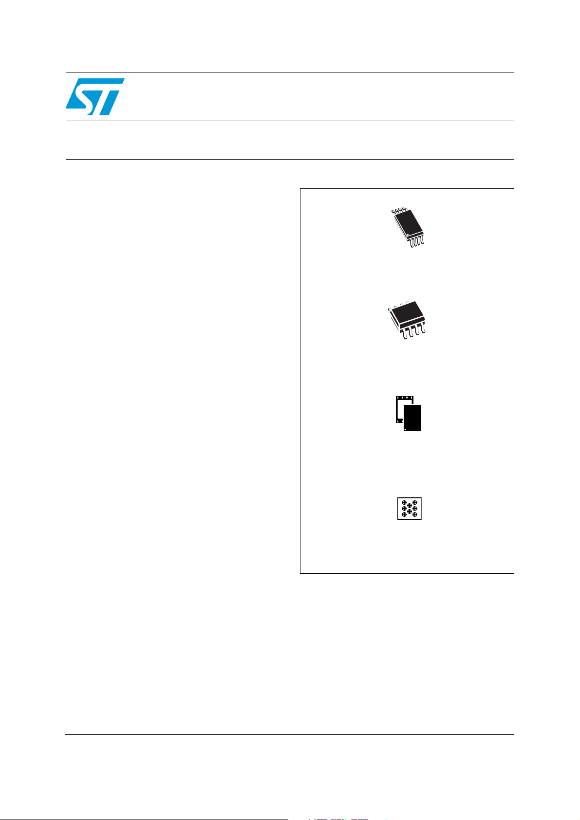
M24256-BW M24256-BR M24256-BF
SO8 (MN)
150 mil width
TSSOP8 (DW)
169 mil width
UFDFPN8
(MC)
WLCSP (CS)
Features
■ Compatible with all I
–1 MHz
– 400 kHz
– 100 kHz
■ Single supply voltage and high speed:
– 1 MHz clock from 1.7 V to 5.5 V
■ Memory array:
– 256 Kbit (32 Kbytes) of EEPROM
– Page size: 64 bytes
– Additional Write lockable page
(M24256-D order codes)
■ Write:
– Byte Write within 5 ms
– Page Write within 5 ms
■ Operating temperature range: from -40-20 °C
up to +85125 °C
■ Random and sequential Read modes
■ Write protect of the whole memory array
■ Enhanced ESD/Latch-Up protection
■ More than 4 million Write cycles
■ More than 200-year data retention
■ Packages:
– RoHS compliant and halogen-free
(ECOPACK
2
®
)
C bus modes:
M24256-DR M24256-DF
256-Kbit serial I²C bus EEPROM
Datasheet − production data
August 2012 Doc ID 6757 Rev 27 1/41
This is information on a product in full production.
www.st.com
1

Contents M24256-BW M24256-BR M24256-BF M24256-DR M24256-DF
Contents
1 Description . . . . . . . . . . . . . . . . . . . . . . . . . . . . . . . . . . . . . . . . . . . . . . . . . 6
2 Signal description . . . . . . . . . . . . . . . . . . . . . . . . . . . . . . . . . . . . . . . . . . . 8
2.1 Serial Clock (SCL) . . . . . . . . . . . . . . . . . . . . . . . . . . . . . . . . . . . . . . . . . . . 8
2.2 Serial Data (SDA) . . . . . . . . . . . . . . . . . . . . . . . . . . . . . . . . . . . . . . . . . . . . 8
2.3 Chip Enable (E2, E1, E0) . . . . . . . . . . . . . . . . . . . . . . . . . . . . . . . . . . . . . . 8
2.4 Write Control (WC
2.5 V
(ground) . . . . . . . . . . . . . . . . . . . . . . . . . . . . . . . . . . . . . . . . . . . . . . . 8
SS
2.6 Supply voltage (V
2.6.1 Operating supply voltage V
2.6.2 Power-up conditions . . . . . . . . . . . . . . . . . . . . . . . . . . . . . . . . . . . . . . . . 9
2.6.3 Device reset . . . . . . . . . . . . . . . . . . . . . . . . . . . . . . . . . . . . . . . . . . . . . . . 9
2.6.4 Power-down conditions . . . . . . . . . . . . . . . . . . . . . . . . . . . . . . . . . . . . . . 9
) . . . . . . . . . . . . . . . . . . . . . . . . . . . . . . . . . . . . . . . . . . . 8
) . . . . . . . . . . . . . . . . . . . . . . . . . . . . . . . . . . . . . . . . . 9
CC
CC . . . . . . . . . . . . . . . . . . . . . . . . . . . . . . . . . . . . . . . . . . 9
3 Memory organization . . . . . . . . . . . . . . . . . . . . . . . . . . . . . . . . . . . . . . . 10
4 Device operation . . . . . . . . . . . . . . . . . . . . . . . . . . . . . . . . . . . . . . . . . . . 11
4.1 Start condition . . . . . . . . . . . . . . . . . . . . . . . . . . . . . . . . . . . . . . . . . . . . . 12
4.2 Stop condition . . . . . . . . . . . . . . . . . . . . . . . . . . . . . . . . . . . . . . . . . . . . . 12
4.3 Data input . . . . . . . . . . . . . . . . . . . . . . . . . . . . . . . . . . . . . . . . . . . . . . . . . 12
4.4 Acknowledge bit (ACK) . . . . . . . . . . . . . . . . . . . . . . . . . . . . . . . . . . . . . . . 12
4.5 Device addressing . . . . . . . . . . . . . . . . . . . . . . . . . . . . . . . . . . . . . . . . . . 13
5 Instructions . . . . . . . . . . . . . . . . . . . . . . . . . . . . . . . . . . . . . . . . . . . . . . . 14
5.1 Write operations . . . . . . . . . . . . . . . . . . . . . . . . . . . . . . . . . . . . . . . . . . . . 14
5.1.1 Byte Write . . . . . . . . . . . . . . . . . . . . . . . . . . . . . . . . . . . . . . . . . . . . . . . 15
5.1.2 Page Write . . . . . . . . . . . . . . . . . . . . . . . . . . . . . . . . . . . . . . . . . . . . . . . 16
5.1.3 Write Identification Page (M24256-D only) . . . . . . . . . . . . . . . . . . . . . . 17
5.1.4 Lock Identification Page (M24256-D only) . . . . . . . . . . . . . . . . . . . . . . . 17
5.1.5 ECC (Error Correction Code) and Write cycling . . . . . . . . . . . . . . . . . . 18
5.1.6 Minimizing Write delays by polling on ACK . . . . . . . . . . . . . . . . . . . . . . 19
5.2 Read operations . . . . . . . . . . . . . . . . . . . . . . . . . . . . . . . . . . . . . . . . . . . . 20
5.2.1 Random Address Read . . . . . . . . . . . . . . . . . . . . . . . . . . . . . . . . . . . . . 20
2/41 Doc ID 6757 Rev 27

M24256-BW M24256-BR M24256-BF M24256-DR M24256-DF Contents
5.2.2 Current Address Read . . . . . . . . . . . . . . . . . . . . . . . . . . . . . . . . . . . . . . 21
5.2.3 Sequential Read . . . . . . . . . . . . . . . . . . . . . . . . . . . . . . . . . . . . . . . . . . 21
5.3 Read Identification Page (M24256-D only) . . . . . . . . . . . . . . . . . . . . . . . 21
5.4 Read the lock status (M24256-D only) . . . . . . . . . . . . . . . . . . . . . . . . . . . 21
6 Initial delivery state . . . . . . . . . . . . . . . . . . . . . . . . . . . . . . . . . . . . . . . . . 22
7 Maximum rating . . . . . . . . . . . . . . . . . . . . . . . . . . . . . . . . . . . . . . . . . . . . 23
8 DC and AC parameters . . . . . . . . . . . . . . . . . . . . . . . . . . . . . . . . . . . . . . 24
9 Package mechanical data . . . . . . . . . . . . . . . . . . . . . . . . . . . . . . . . . . . . 33
10 Part numbering . . . . . . . . . . . . . . . . . . . . . . . . . . . . . . . . . . . . . . . . . . . . 38
11 Revision history . . . . . . . . . . . . . . . . . . . . . . . . . . . . . . . . . . . . . . . . . . . 39
Doc ID 6757 Rev 27 3/41

List of tables M24256-BW M24256-BR M24256-BF M24256-DR M24256-DF
List of tables
Table 1. Signal names . . . . . . . . . . . . . . . . . . . . . . . . . . . . . . . . . . . . . . . . . . . . . . . . . . . . . . . . . . . . 6
Table 2. Device select code . . . . . . . . . . . . . . . . . . . . . . . . . . . . . . . . . . . . . . . . . . . . . . . . . . . . . . . 13
Table 3. Most significant address byte . . . . . . . . . . . . . . . . . . . . . . . . . . . . . . . . . . . . . . . . . . . . . . . 14
Table 4. Least significant address byte . . . . . . . . . . . . . . . . . . . . . . . . . . . . . . . . . . . . . . . . . . . . . . 14
Table 5. Absolute maximum ratings . . . . . . . . . . . . . . . . . . . . . . . . . . . . . . . . . . . . . . . . . . . . . . . . . 23
Table 6. Operating conditions (voltage range W) . . . . . . . . . . . . . . . . . . . . . . . . . . . . . . . . . . . . . . . 24
Table 7. Operating conditions (voltage range R) . . . . . . . . . . . . . . . . . . . . . . . . . . . . . . . . . . . . . . . 24
Table 8. Operating conditions (voltage range F) . . . . . . . . . . . . . . . . . . . . . . . . . . . . . . . . . . . . . . . 24
Table 9. AC measurement conditions. . . . . . . . . . . . . . . . . . . . . . . . . . . . . . . . . . . . . . . . . . . . . . . . 24
Table 10. Input parameters. . . . . . . . . . . . . . . . . . . . . . . . . . . . . . . . . . . . . . . . . . . . . . . . . . . . . . . . . 25
Table 11. Cycling performance by groups of four bytes . . . . . . . . . . . . . . . . . . . . . . . . . . . . . . . . . . . 25
Table 12. Memory cell data retention . . . . . . . . . . . . . . . . . . . . . . . . . . . . . . . . . . . . . . . . . . . . . . . . . 25
Table 13. DC characteristics (M24256-BW, device grade 6) . . . . . . . . . . . . . . . . . . . . . . . . . . . . . . . 26
Table 14. DC characteristics (M24256-BR, M24256-DR, device grade 6) . . . . . . . . . . . . . . . . . . . . . 27
Table 15. DC characteristics (M24256-BF, M24256-DF, device grade 6) . . . . . . . . . . . . . . . . . . . . . 28
Table 16. 400 kHz AC characteristics. . . . . . . . . . . . . . . . . . . . . . . . . . . . . . . . . . . . . . . . . . . . . . . . . 29
Table 17. 1 MHz AC characteristics . . . . . . . . . . . . . . . . . . . . . . . . . . . . . . . . . . . . . . . . . . . . . . . . . . 30
Table 18. TSSOP8 – 8-lead thin shrink small outline, package mechanical data. . . . . . . . . . . . . . . . 33
Table 19. SO8N – 8 lead plastic small outline, 150 mils body width, package data. . . . . . . . . . . . . . 34
Table 20. UFDFPN8 (MLP8) 8-lead ultra thin fine pitch dual flat package no lead
2 x 3 mm, data . . . . . . . . . . . . . . . . . . . . . . . . . . . . . . . . . . . . . . . . . . . . . . . . . . . . . . . . . . 35
Table 21. M24256-DFCS6TP/K, WLCSP 8-bump wafer-level chip scale package mechanical data. 37
Table 22. Ordering information scheme . . . . . . . . . . . . . . . . . . . . . . . . . . . . . . . . . . . . . . . . . . . . . . . 38
Table 23. Document revision history . . . . . . . . . . . . . . . . . . . . . . . . . . . . . . . . . . . . . . . . . . . . . . . . . 39
4/41 Doc ID 6757 Rev 27

M24256-BW M24256-BR M24256-BF M24256-DR M24256-DF List of figures
List of figures
Figure 1. Logic diagram . . . . . . . . . . . . . . . . . . . . . . . . . . . . . . . . . . . . . . . . . . . . . . . . . . . . . . . . . . . . 6
Figure 2. 8-pin package connections . . . . . . . . . . . . . . . . . . . . . . . . . . . . . . . . . . . . . . . . . . . . . . . . . . 7
Figure 3. WLCSP connections (top view, marking side, with balls on the underside) . . . . . . . . . . . . . 7
Figure 4. Device select code . . . . . . . . . . . . . . . . . . . . . . . . . . . . . . . . . . . . . . . . . . . . . . . . . . . . . . . . 8
Figure 5. Block diagram . . . . . . . . . . . . . . . . . . . . . . . . . . . . . . . . . . . . . . . . . . . . . . . . . . . . . . . . . . . 10
Figure 6. I
Figure 7. Write mode sequences with WC
Figure 8. Write mode sequences with WC
Figure 9. Write cycle polling flowchart using ACK . . . . . . . . . . . . . . . . . . . . . . . . . . . . . . . . . . . . . . . 19
Figure 10. Read mode sequences . . . . . . . . . . . . . . . . . . . . . . . . . . . . . . . . . . . . . . . . . . . . . . . . . . . . 20
Figure 11. AC measurement I/O waveform . . . . . . . . . . . . . . . . . . . . . . . . . . . . . . . . . . . . . . . . . . . . . 24
Figure 12. Maximum R
Figure 13. Maximum R
Figure 14. AC waveforms . . . . . . . . . . . . . . . . . . . . . . . . . . . . . . . . . . . . . . . . . . . . . . . . . . . . . . . . . . 32
Figure 15. TSSOP8 – 8-lead thin shrink small outline, package outline . . . . . . . . . . . . . . . . . . . . . . . 33
Figure 16. SO8N – 8 lead plastic small outline, 150 mils body width, package outline . . . . . . . . . . . . 34
Figure 17. UFDFPN8 (MLP8) - 8-lead ultra thin fine pitch dual flat no lead, package outline . . . . . . . 35
Figure 18. M24256-DFCS6TP/K, WLCSP 8-bump wafer-level chip scale package outline . . . . . . . . 36
2
C bus protocol . . . . . . . . . . . . . . . . . . . . . . . . . . . . . . . . . . . . . . . . . . . . . . . . . . . . . . . . . 11
= 0 (data write enabled) . . . . . . . . . . . . . . . . . . . . . . . . . 15
= 1 (data write inhibited) . . . . . . . . . . . . . . . . . . . . . . . . . 16
value versus bus parasitic capacitance (C
2
an I
C bus at maximum frequency fC = 400 kHz . . . . . . . . . . . . . . . . . . . . . . . . . . . . . . . . 31
2
an I
C bus at maximum frequency fC = 1MHz . . . . . . . . . . . . . . . . . . . . . . . . . . . . . . . . . . 31
bus
value versus bus parasitic capacitance C
bus
bus
bus
) for
) for
Doc ID 6757 Rev 27 5/41
Description M24256-BW M24256-BR M24256-BF M24256-DR M24256-DF
!)F
%% 3$!
6
##
-XXX
7#
3#,
6
33
1 Description
The M24256 is a 256-Kbit I2C-compatible EEPROM (Electrically Erasable PROgrammable
Memory) organized as 32 K × 8 bits.
The M24256-BW can operate with a supply voltage from 2.5 V to 5.5 V, the M24256-BR and
M24256-DR can operate with a supply voltage from 1.8 V to 5.5 V, and the M24256-BF and
M24256-DF can operate with a supply voltage from 1.7 V to 5.5 V. All these devices operate
with a clock frequency of 1 MHz (or less), over an ambient temperature range of –40 °C /
+85 °C.
The M24256-Dx offers an additional page, named the Identification Page (64 bytes). The
Identification Page can be used to store sensitive application parameters which can be
(later) permanently locked in Read-only mode.
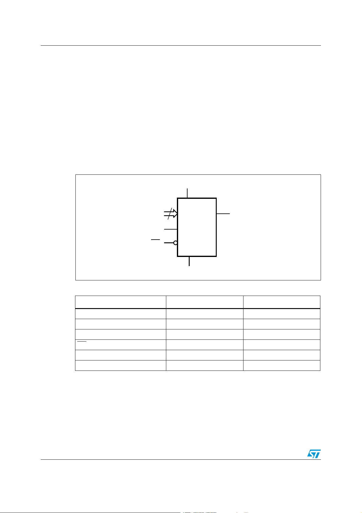
Figure 1. Logic diagram
Table 1. Signal names
Signal name Function Direction
E2, E1, E0 Chip Enable Input
SDA Serial Data I/O
SCL Serial Clock Input
WC
V
CC
V
SS
6/41 Doc ID 6757 Rev 27
Write Control Input
Supply voltage
Ground
M24256-BW M24256-BR M24256-BF M24256-DR M24256-DF Description
3$!6
33
3#,
7#%
% 6
##
%
!)F
-36
%
%
%
7#
6
##
3#,
3$!
6
33
Figure 2. 8-pin package connections
1. DU: Don't Use (if connected, must be connected to VSS)
2. See Section 9: Package mechanical data for package dimensions, and how to identify pin 1.
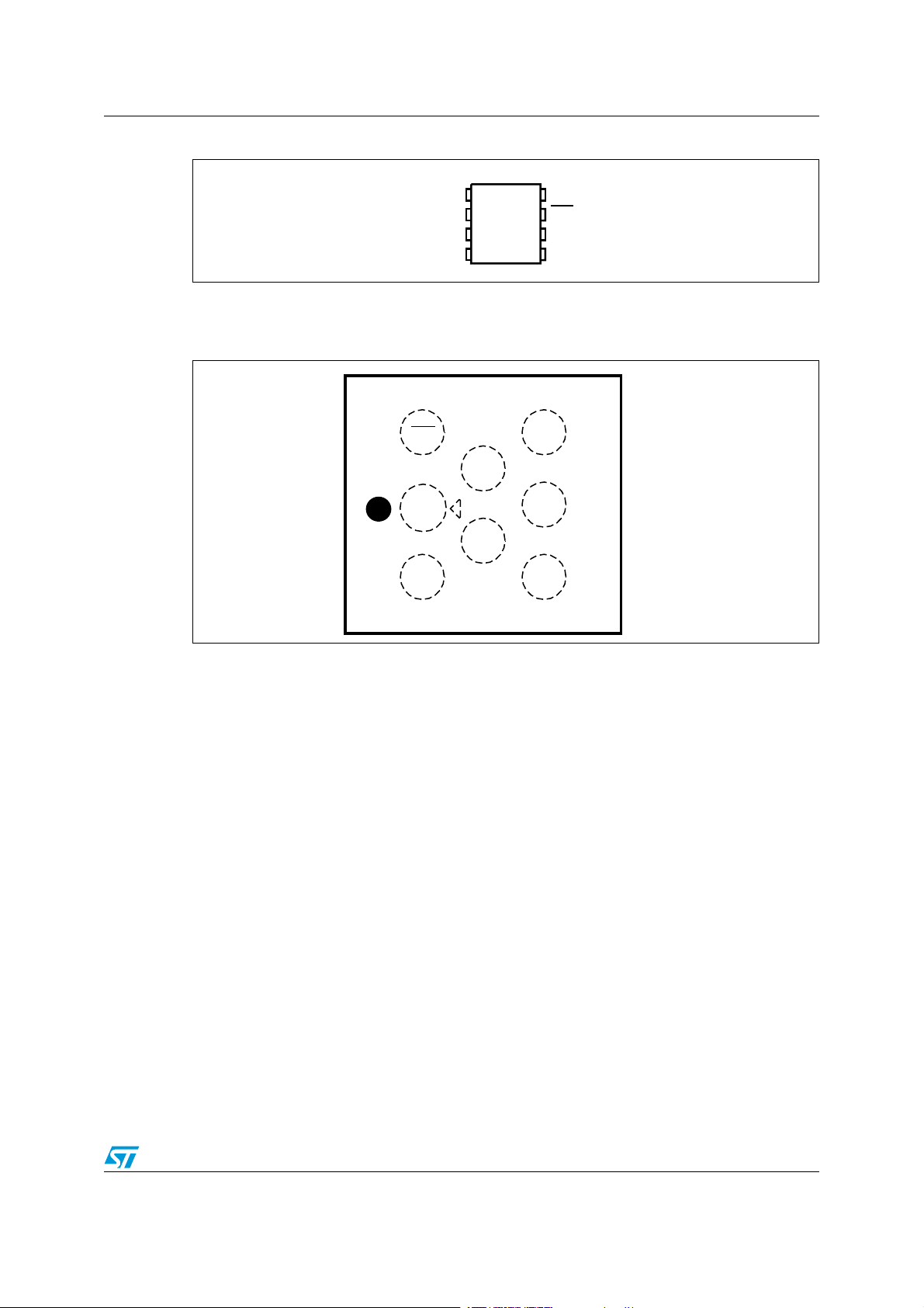
Figure 3. WLCSP connections (top view, marking side, with balls on the underside)
Caution: As EEPROM cells lose their charge (and so their binary value) when exposed to ultra violet
(UV) light, EEPROM dice delivered in wafer form or in WLCSP package by
STMicroelectronics must never be exposed to UV light.
Doc ID 6757 Rev 27 7/41
Signal description M24256-BW M24256-BR M24256-BF M24256-DR M24256-DF
Ai12806
V
CC
M24xxx
V
SS
E
i
V
CC
M24xxx
V
SS
E
i
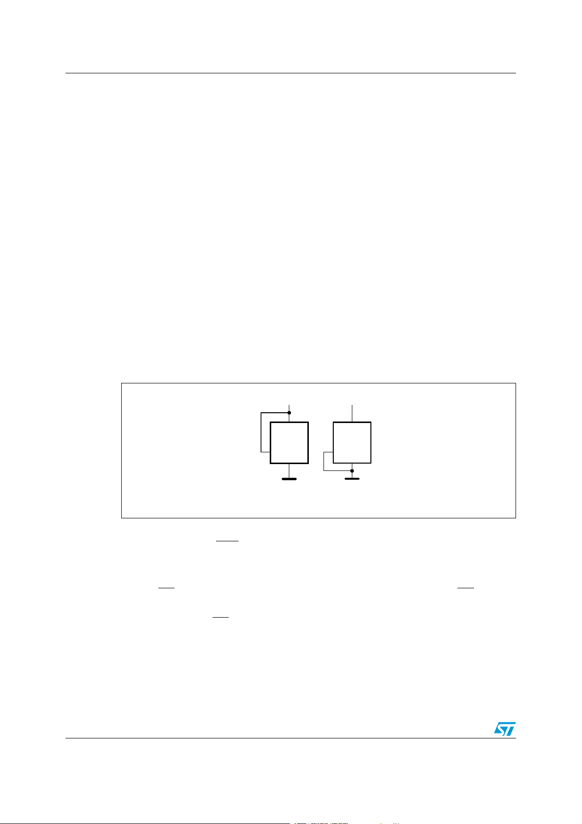
2 Signal description
2.1 Serial Clock (SCL)
The signal applied on the SCL input is used to strobe the data available on SDA(in) and to
output the data on SDA(out).
2.2 Serial Data (SDA)
SDA is an input/output used to transfer data in or data out of the device. SDA(out) is an open
drain output that may be wire-OR’ed with other open drain or open collector signals on the
bus. A pull-up resistor must be connected from Serial Data (SDA) to V
indicates how to calculate the value of the pull-up resistor).
2.3 Chip Enable (E2, E1, E0)
(E2,E1,E0) input signals are used to set the value that is to be looked for on the three least
significant bits (b3, b2, b1) of the 7-bit device select code (see Ta b le 2 ). These inputs must
be tied to V
are read as low (0).
or VSS, as shown in Figure 4. When not connected (left floating), these inputs
CC
(Figure 12
CC
Figure 4. Device select code
2.4 Write Control (WC)
This input signal is useful for protecting the entire contents of the memory from inadvertent
write operations. Write operations are disabled to the entire memory array when Write
Control (WC
driven low or left floating.
When Write Control (WC
acknowledged, Data bytes are not acknowledged.
) is driven high. Write operations are enabled when Write Control (WC) is either
) is driven high, device select and address bytes are
2.5 VSS (ground)
VSS is the reference for the VCC supply voltage.
8/41 Doc ID 6757 Rev 27

M24256-BW M24256-BR M24256-BF M24256-DR M24256-DF Signal description
2.6 Supply voltage (VCC)
2.6.1 Operating supply voltage V
Prior to selecting the memory and issuing instructions to it, a valid and stable VCC voltage
within the specified [V
(min), VCC(max)] range must be applied (see Operating conditions
CC
in Section 8: DC and AC parameters). In order to secure a stable DC supply voltage, it is
recommended to decouple the V
10 nF to 100 nF) close to the V
CC
CC/VSS
This voltage must remain stable and valid until the end of the transmission of the instruction
and, for a write instruction, until the completion of the internal write cycle (t
2.6.2 Power-up conditions
The VCC voltage has to rise continuously from 0 V up to the minimum VCC operating voltage
(see Operating conditions in Section 8: DC and AC parameters) and the rise time must not
vary faster than 1 V/µs.
2.6.3 Device reset
In order to prevent inadvertent write operations during power-up, a power-on-reset (POR)
circuit is included.
At power-up, the device does not respond to any instruction until V
internal reset threshold voltage. This threshold is lower than the minimum V
voltage (see Operating conditions in Section 8: DC and AC parameters). When V
over the POR threshold, the device is reset and enters the Standby Power mode; however,
the device must not be accessed until V
specified [V
parameters).
(min), VCC(max)] range (see Operating conditions in Section 8: DC and AC
CC
CC
line with a suitable capacitor (usually of the order of
package pins.
).
W
has reached the
CC
reaches a valid and stable DC voltage within the
CC
operating
CC
CC
passes
In a similar way, during power-down (continuous decrease in V
accessed when V
drops below VCC(min). When VCC drops below the power-on-reset
CC
threshold voltage, the device stops responding to any instruction sent to it.
2.6.4 Power-down conditions
During power-down (continuous decrease in VCC), the device must be in the Standby Power
mode (mode reached after decoding a Stop condition, assuming that there is no internal
write cycle in progress).
), the device must not be
CC
Doc ID 6757 Rev 27 9/41
Memory organization M24256-BW M24256-BR M24256-BF M24256-DR M24256-DF
-36
7#
#ONTROLLOGIC
(IGHVOLTAGE
GENERATOR
)/SHIFTREGISTER
!DDRESSREGISTER
ANDCOUNTER
$ATA
REGISTER
PAGE
8DECODER
9DECODER
)DENTIFICATIONPAGE
%
%
3#,
3$!
%
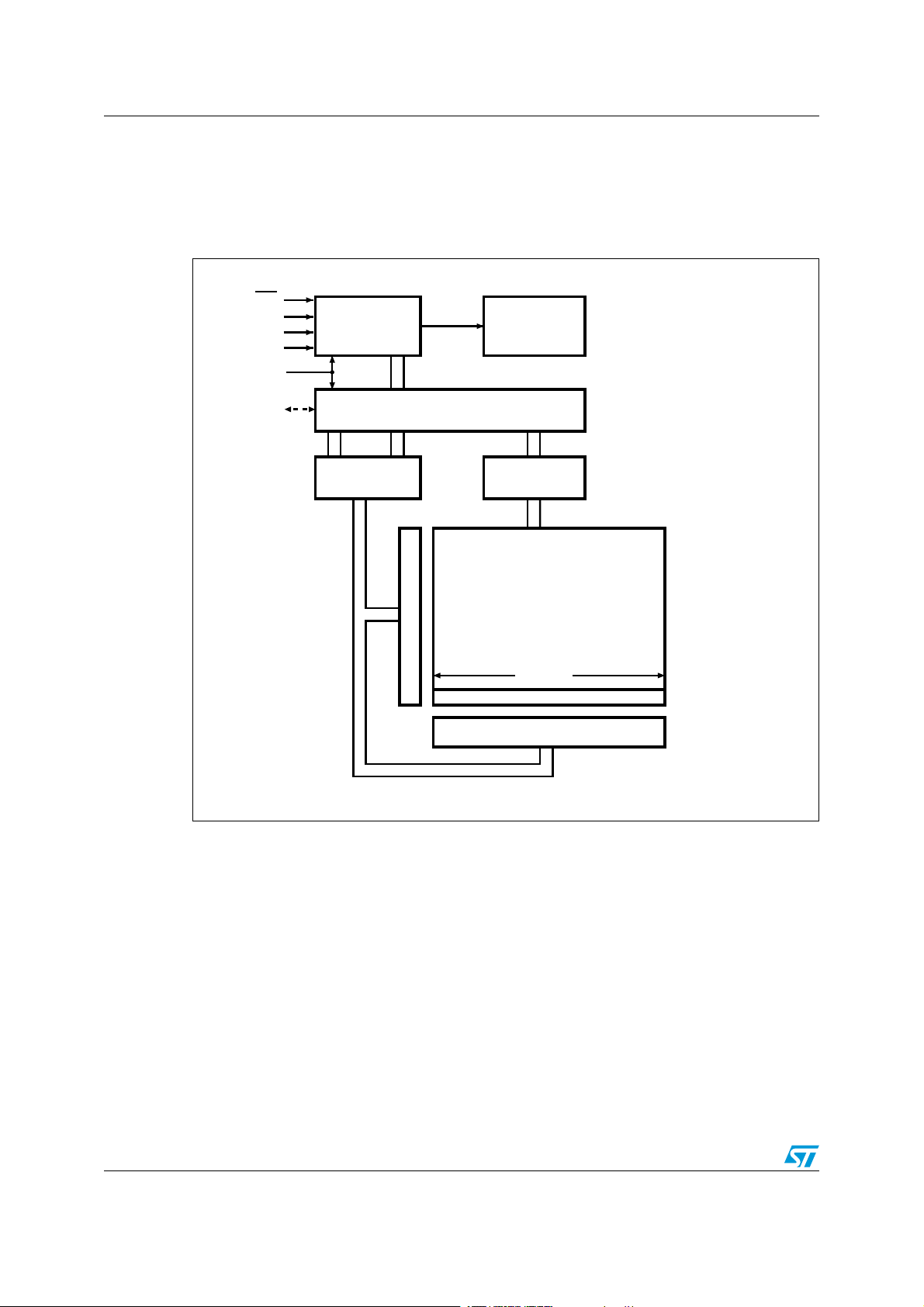
3 Memory organization
The memory is organized as shown below.
Figure 5. Block diagram
10/41 Doc ID 6757 Rev 27
M24256-BW M24256-BR M24256-BF M24256-DR M24256-DF Device operation
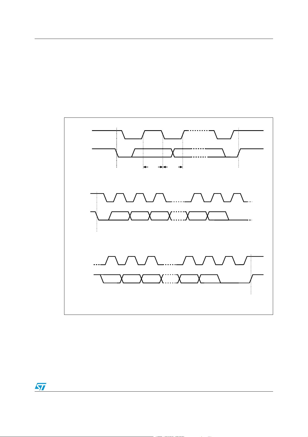
SCL
SDA
SCL
SDA
SDA
START
Condition
SDA
Input
SDA
Change
AI00792B
STOP
Condition
1 23 7 89
MSB
ACK
START
Condition
SCL
1 23 7 89
MSB ACK
STOP
Condition
4 Device operation
The device supports the I2C protocol. This is summarized in Figure 6. Any device that sends
data on to the bus is defined to be a transmitter, and any device that reads the data to be a
receiver. The device that controls the data transfer is known as the bus master, and the
other as the slave device. A data transfer can only be initiated by the bus master, which will
also provide the serial clock for synchronization. The device is always a slave in all
communications.
Figure 6. I
2
C bus protocol
Doc ID 6757 Rev 27 11/41

Device operation M24256-BW M24256-BR M24256-BF M24256-DR M24256-DF
4.1 Start condition
Start is identified by a falling edge of Serial Data (SDA) while Serial Clock (SCL) is stable in
the high state. A Start condition must precede any data transfer instruction. The device
continuously monitors (except during a Write cycle) Serial Data (SDA) and Serial Clock
(SCL) for a Start condition.
4.2 Stop condition
Stop is identified by a rising edge of Serial Data (SDA) while Serial Clock (SCL) is stable
and driven high. A Stop condition terminates communication between the device and the
bus master. A Read instruction that is followed by NoAck can be followed by a Stop
condition to force the device into the Standby mode.
A Stop condition at the end of a Write instruction triggers the internal Write cycle.
4.3 Data input
During data input, the device samples Serial Data (SDA) on the rising edge of Serial Clock
(SCL). For correct device operation, Serial Data (SDA) must be stable during the rising edge
of Serial Clock (SCL), and the Serial Data (SDA) signal must change only when Serial Clock
(SCL) is driven low.
4.4 Acknowledge bit (ACK)
The acknowledge bit is used to indicate a successful byte transfer. The bus transmitter,
whether it be bus master or slave device, releases Serial Data (SDA) after sending eight bits
of data. During the 9
acknowledge the receipt of the eight data bits.
th
clock pulse period, the receiver pulls Serial Data (SDA) low to
12/41 Doc ID 6757 Rev 27
M24256-BW M24256-BR M24256-BF M24256-DR M24256-DF Device operation
4.5 Device addressing
To start communication between the bus master and the slave device, the bus master must
initiate a Start condition. Following this, the bus master sends the device select code, shown
in Ta ble 2 (on Serial Data (SDA), most significant bit first).
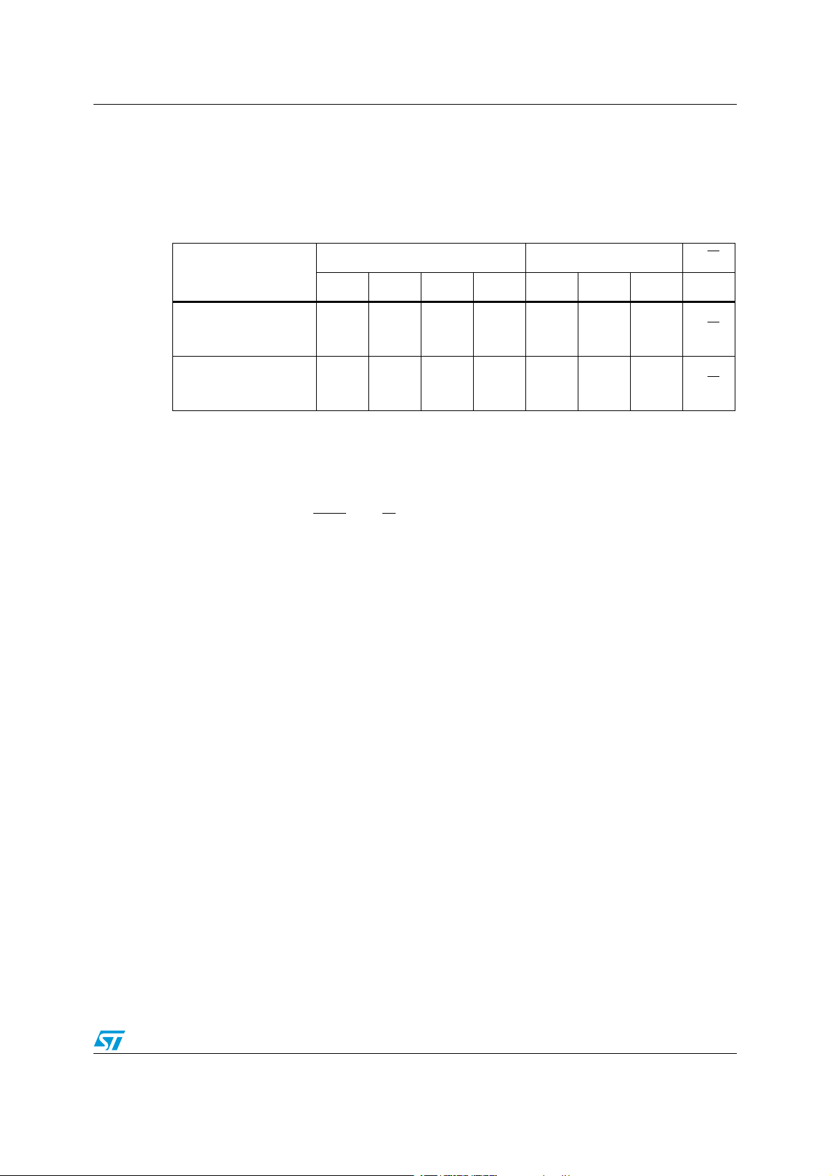
Table 2. Device select code
Device type identifier
b7 b6 b5 b4 b3 b2 b1 b0
Device select code
when addressing the
memory array
Device select code
when accessing the
Identification page
1. The most significant bit, b7, is sent first.
2. E0, E1 and E2 are compared against the respective external pins on the memory device.
1010E2E1E0RW
1011E2E1E0RW
(1)
Chip Enable address
When the device select code is received, the device only responds if the Chip Enable
Address is the same as the value on the Chip Enable (E2, E1, E0) inputs.
th
The 8
bit is the Read/Write bit (RW). This bit is set to 1 for Read and 0 for Write operations.
(2)
RW
If a match occurs on the device select code, the corresponding device gives an
acknowledgment on Serial Data (SDA) during the 9
th
bit time. If the device does not match
the device select code, it deselects itself from the bus, and goes into Standby mode.
Doc ID 6757 Rev 27 13/41
 Loading...