

查询M24256-AW 供应商
This device is now designated as “Not for New Design”. Please use the M24256-B in all future designs (as described in application note AN1470).
■ Compat ible with I
■ Two Wire I
Supports 400 kHz Protocol
■ Single Supply Voltage:
– 4.5V to 5.5V for M24256-A
– 2.5V to 5.5V for M24256-AW
■ 2 Chip Enable Inputs: up to four memories can
be connected to the same I
■ Hardware Write Control
■ BYTE and PAGE WRITE (up to 64 Bytes)
■ RANDOM and SEQUENTIAL READ Modes
■ Self-Tim ed P ro g ra m ming Cycle
■ Automatic Address Incrementing
■ Enhanced ESD/Latch-Up Behavior
■ More than 100,000 Erase/Write Cycles
■ More than 40 Year Data Retention
2
C Extended Addressing
2
C Serial Interface
2
C bus
M24256-A
256 Kbit Serial I²C Bus EEPROM
With Two Chip En able Lin es
NOT FOR NEW DESIGN
8
TSSOP14 (DL)
169 mil width
1
PDIP8 (BN)
0.25 mm frame
8
1
SO8 (MN)
150 mil width
SBGA
SBGA7 (EA)
140 x 90 mil
8
1
SO8 (MW)
200 mil width
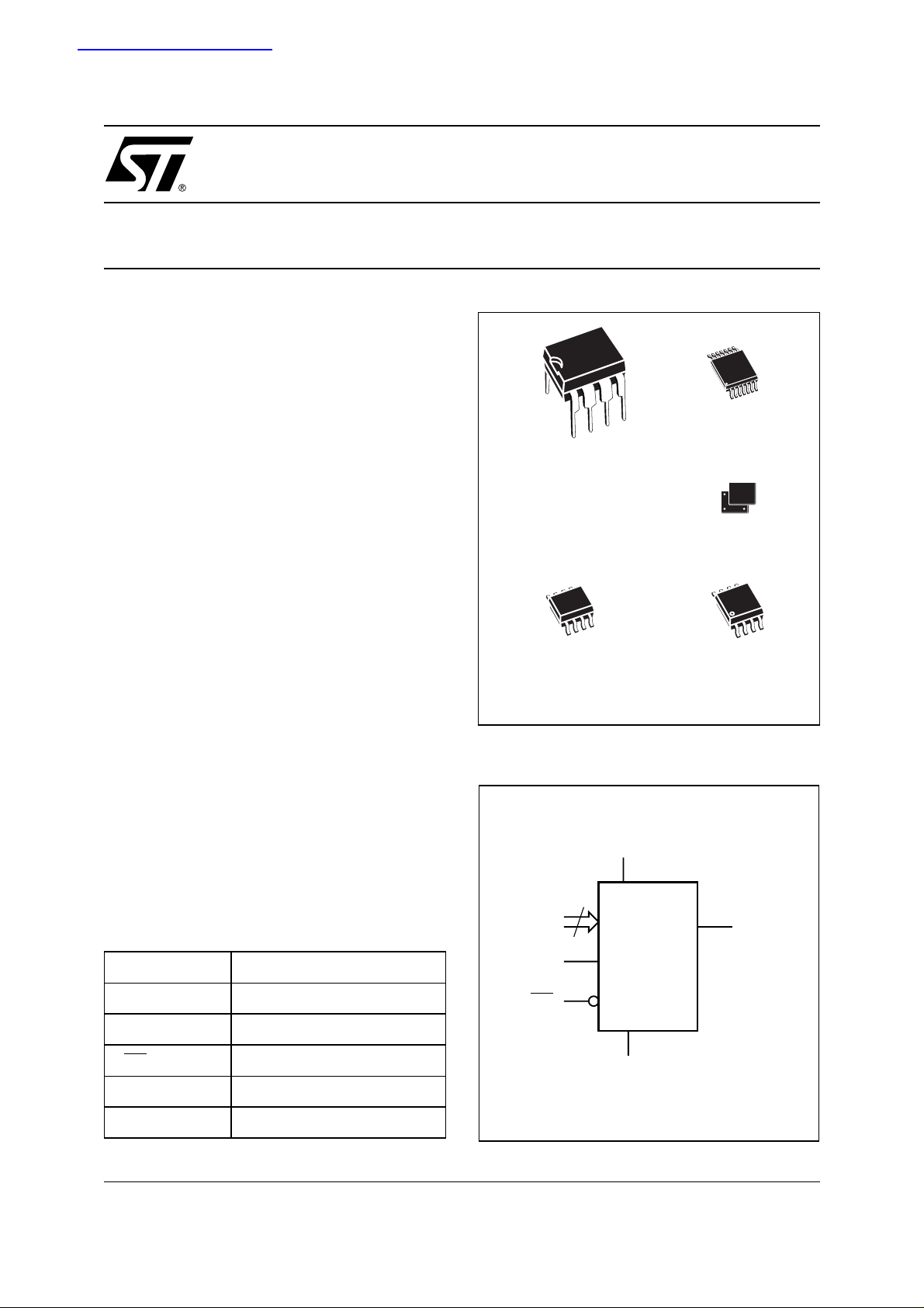
DESCRIPTION
These I
2
C-compatible electrically erasable pro-
Figure 1. Logic Diagram
grammable memory (EEPROM) devices are organized as 32Kx8 bits, and operate down to 2. 5V
(for the M24256-AW).
The M24256-A is available in Plastic Dual-in-Line,
Plastic Small Outline and Thin Shrink Small Out-
Table 1. Signal Names
E0, E1 Chip Enable
SDA Serial Data
SCL Serial Clock
WC
V
CC
V
SS
November 2001
This is information on a product still in production but not recommended for new designs.
Write Control
Supply Voltage
Ground
E0-E1
SCL
WC
2
V
CC
M24256-A
V
SS
SDA
AI02271C
1/20
M24256-A
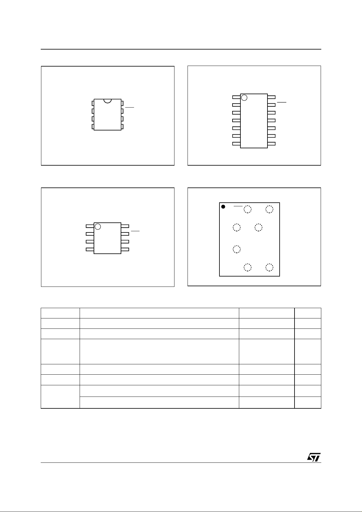
Figure 2A. DIP Connections
M24256-A
1
E0 V
2
3
NC
4
SS
AI02273C
Note: 1. NC = Not Connected
Figure 2B. SO C on ne ct i on s
M24256-A
E0 V
NC
SS
1
2
3
4
AI02272C
Figure 2C. TSSOP Connections
M24256-A
1
2
3
4
5
6
7
14
13
12
11
10
9
8
AI02388C
V
CC
WC
NC
NC
NC
SDAV
8
CC
7
WCE1
6
SCL
5
SDAV
E1
NC
NC
NC
NC SCL
SS
Note: 1. NC = Not Connected
E0
Figure 2D. SB GA Connections (t o p v ie w)
M24256-A
S0
S1
V
SS
AI03760
WC
8
CC
7
WCE1
6
SCL
5
SDAV
V
CC
SDA
SCL
Note: 1. NC = Not Connected
Table 2. Absolute Maximum Ratings
1
Symbol Parameter Value Unit
T
A
T
STG
T
LEAD
V
IO
V
CC
V
ESD
Note: 1. Exc ept for the rating “Operating Temperature Ra nge”, stres ses above those listed in the Table “Absolute Maximum Ratings” may
cause permanent damage to the device. These are stress ratings only, and operation of the device at these or any other conditions
above those indi cated in t he Operating sect i ons of thi s specifi cation i s not impl i ed. Exposure to Absolute M aximum Rating c onditions for extended periods may affect device reliability. Refer also to the ST SURE Program and other relevant quality documents.
2. IPC/ JEDEC J-STD-020A
3. JED EC St d JESD22-A 114A (C1=1 00 pF, R1=1500 Ω, R2=500 Ω)
4. EIA J I C-121 (Condition C) (200 pF, 0 Ω)
Ambient Operating Temperature –40 to 125 °C
Storage Temperature –65 to 150 °C
Lead Temperature during Soldering
PDIP: 10 seconds
SO: 20 seconds (max)
2
TSSOP: 20 seconds (max)
2
260
235
235
°C
Input or Output range –0.6 to 6.5 V
Supply Voltage –0.3 to 6.5 V
Electrostatic Discharge Voltage (Human Body model)
Electrostatic Discharge Voltage (Machine model)
4
3
4000 V
200 V
2/20
M24256-A
line packages. The M 24256-A is al so available in
a chip-scale (SBGA) package.
These memory devices are compatible with the
2
I
C extended memory standard. This is a two wire
serial interface that uses a bi-directiona l data bus
and serial clock. The memory carries a built-in 4bit unique Device Type Identifier code (1010) in
accordance with the I
The memory behaves as a slave device in the I
2
C bus definition.
2
protocol, with all memory operations synchronized
by the serial clock. Read and Write operations are
initiated by a START condition, gene rated by the
bus master. The START condition is followed by a
Device Select Code and RW
bit (as described in
Table 3), terminated by an acknowledge bit.
When writing data to the memory, the mem ory in-
serts an acknowledge bit during the 9
th
bit time,
following the bus master’s 8-bit transmission.
When data is read by the bus master, the bus
master acknowledges the receipt of the data byte
in the same way. Data transfers are terminated by
a STOP condition after an Ack for WRITE, and after a NoAck for READ.
Power On Reset: V
Lock-Out Write Protect
CC
In order to prevent data corruption and inadvertent
write operations during power up, a Power On Reset (POR) circuit is included. The internal reset is
held active until the V
voltage has reached the
CC
POR threshold value, and all operations are disabled – the device will not respond to any command. In the same way, when V
drops from the
CC
operating voltage, below the POR threshold value,
all operations are disabled and the device will not
respond to any com ma nd. A s table a nd v alid V
CC
must be applied before applying any logic signal.
SIGNAL DESCRIPTION
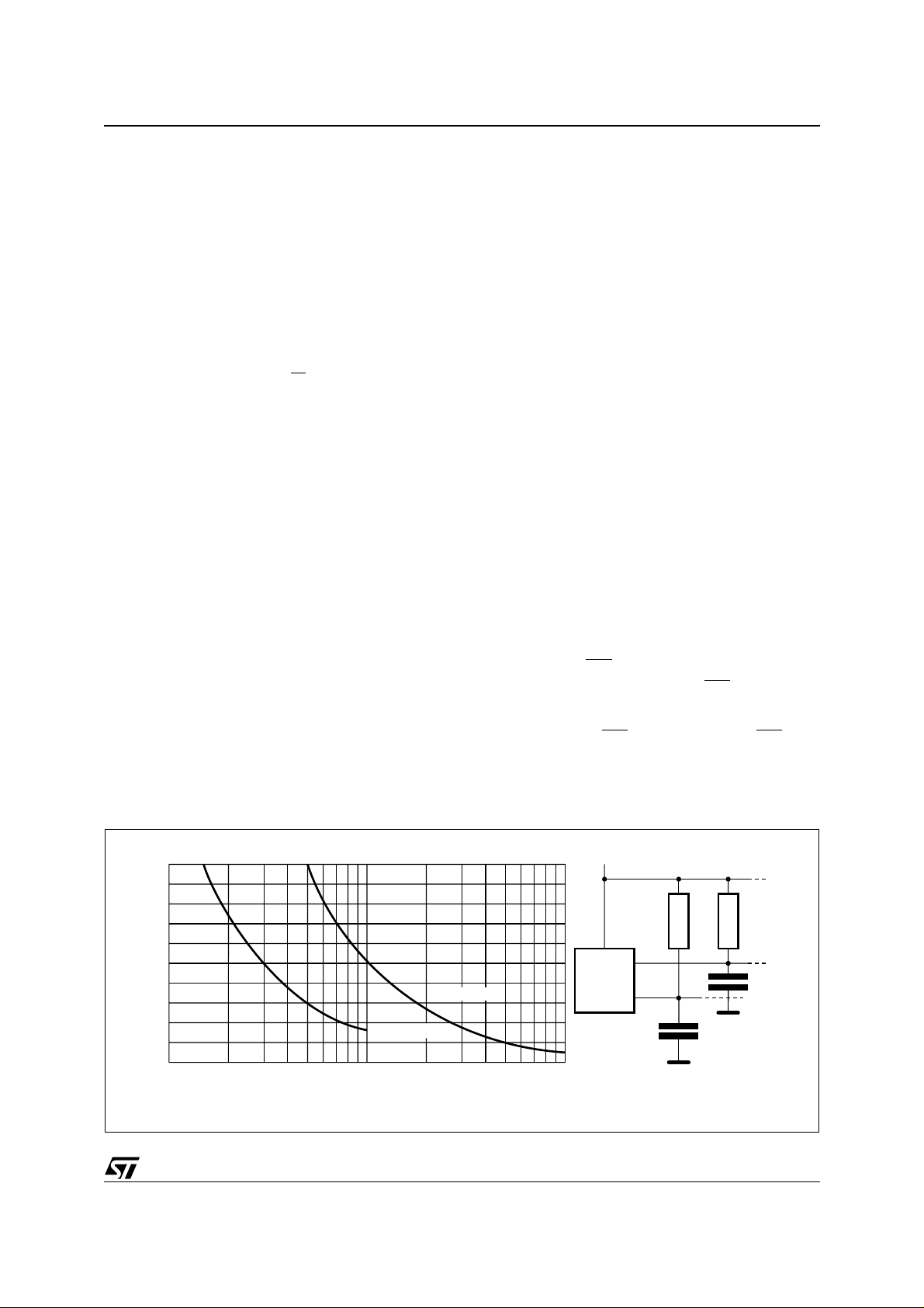
Serial Clock (SCL)
The SCL input pin is used to strobe all data in and
out of the memory. In applications where this line
is used by slaves to synchronize the bus to a slower clock, the master must have an open drain output, and a pull-up resistor must be connected from
the SCL line to V
C
value of the pull-up res istor c an be calculated). In
. (Figure 3 indicates how the
CC
most applications, though, this method of synchronization is not employed, and so the pull-up resistor is not necessary, provided that the master has
a push-pull (rather than open drain) output.
Serial Data (SDA)
The SDA pin is bi-directional, and is used to transfer data in or out of the memory. It is an open drain
output that may be wire-OR’ed with other open
drain or open collector signals on the bus. A pull
up resistor must be connected from the SDA bus
. (Figure 3 indicates how the value of the
to V
CC
pull-up resistor can be calculated).
Chip Enable (E1, E0)
These chip enable inputs are used to set the value
that is to be looked for on th e two least s ignificant
bits (b2, b1) of the 7-bit device select code. These
inputs must be t ied t o V
or VSS to establish the
CC
device select code. When unconnected, the E1
and E0 inputs are internally read as V
7 and Table 8)
Write Control (WC
)
The hardware Write Control pin (WC
protecting the entire contents of the memory from
inadvertent erase/write. The Write Control signal is
used to enable (WC
=VIL) or disable (WC=VIH)
write instructions to the entire memory area. When
(see Table
IL
) is useful for
Figure 3. Maximum R
20
16
12
8
Maximum RP value (kΩ)
4
0
10 1000
Value versus Bus Capacitance (C
L
fc = 100kHz
fc = 400kHz
100
C
(pF)
BUS
) for an I2C Bus
BUS
MASTER
V
CC
R
SDA
SCL
R
C
BUS
L
C
BUS
AI01665
3/20
L
M24256-A
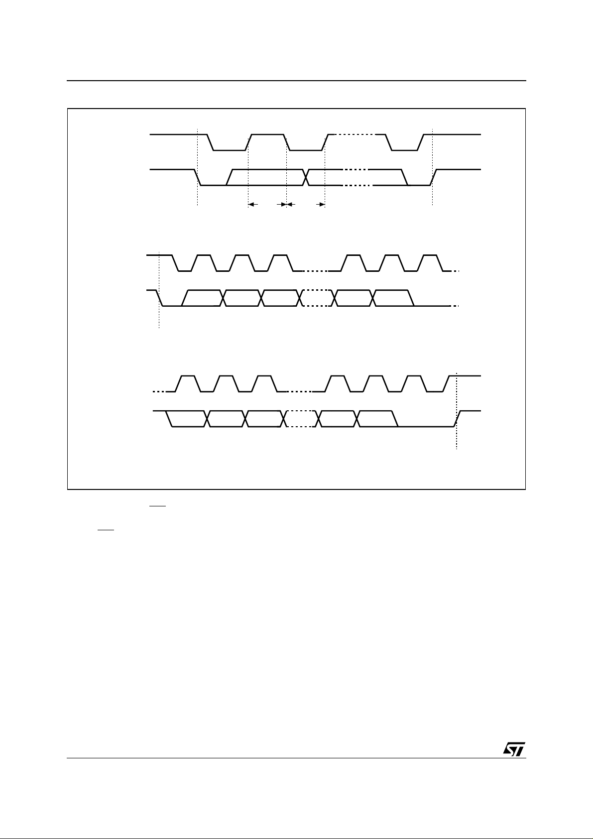
Figure 4. I
2
C Bus Protocol
SCL
SDA
SCL
SDA
START
Condition
SCL
START
Condition
1 23 789
MSB
1 23 789
SDA
Input
SDA
Change
STOP
Condition
ACK
SDA
MSB ACK
unconnected, the WC input is internally read as
V
, and write operations are allowed.
IL
When WC
=1, Device Select and Address bytes
are acknowledged, Data bytes are not acknowledged.
Please see the Application Note
AN404
for a more
detailed description of the Write Control feature.
DEVICE OPERATION
2
The memory device supports the I
C protocol.
This is summarized in Figure 4, and is compared
with other serial bus protocols in Application Note
AN1001
. Any device that sends data on to the bus
is defined to be a transm itter, and any device that
reads the data to be a receiver. The device that
controls the data transfer is k nown as the master,
and the other as the slave. A data transfer can only
be initiated by the mas ter, which wi ll also provide
the serial clock for synchronization. The memory
STOP
Condition
AI00792B
device is always a slave device in all comm unication.
Start Condition
START is identified by a high t o low transition of
the SDA line while the clock, SCL, is s table i n t he
high state. A START condition must precede any
data transfer comman d. Th e m em ory devi ce continuously monitors (except during a program ming
cycle) the SDA and SCL lines for a START condition, and will not respond unless one is given.
Stop Condition
STOP is identified by a low to high transition of the
SDA line wh ile th e clock S CL is sta ble in the h igh
state. A STO P condition terminates c ommunication between the memory device and the bus master. A STOP condition at the end of a Read
command, after (and only after) a NoAck, forces
the memory device into its standby state. A STOP
condition at the end of a Write command triggers
the interna l EEPRO M write cycle.
4/20
M24256-A
Table 3. Device Select Code
b7 b6 b5 b4 b3 b2 b1 b0
Device Select Code 1 0 1 0 0 E1 E0 RW
Note: 1. The most significant bit, b7, is sent firs t.
Acknowledge Bit (ACK)
An acknowledge signal is used to indicate a successful byte transfer. The bus transmitter, whether
it be master or slave, releases the SDA bus after
sending eight bits of data. During the 9
pulse period, the receiver pulls the SDA bus low to
acknowledge the receipt of the eight data bits.
1
Device Type Identifier Chip Enable RW
Table 4. Most Significant Byte
b15 b14 b13 b12 b11 b10 b9 b8
Note: 1. b15 is tr eated as Don’t Care on the M24256-A ser i es.
th
clock
Table 5. Least Significant Byte
b7 b6 b5 b4 b3 b2 b1 b0
Data Input
During data input, the memory device samples the
SDA bus signal on the rising edge of the clock,
SCL. For correct device operation, the SDA signal
must be stable during the clock low-to-high transi-
only
tion, and the data must change
when the SCL
line is low.
Memory Addressing
To start communication betwee n the bus master
and the slave memory, the master must initiate a
START condition. Following this, the master sends
the 8-bit byte, shown in Table 3, on the SDA bus
line (most significant bit first). This consists of the
7-bit Device Select Code, and the 1-bit Read/Write
Designator (RW). The Device Select Code i s further su bd iv i d ed i n to : a 4 - bi t De vi c e T y pe I den t ifier,
and a 3-bit Chip Enable “Address” (0, E1, E0).
To address the memory array, the 4-bit Device
Type Identifier is 1010b.
Up to four memory devices can be connected on a
single I
2
C bus. Each one is given a unique 2-bit
code on its Chip Enable inputs. When the Device
Select Code is received on the SDA bus, the memory only responds if the Chip Select Code is the
same as the pattern applied to its Chip Enable
th
The 8
bit is th e RW bit. This is set to ‘1’ for read
and ‘0’ for write operations. If a match occurs on
the Device Select Cod e, th e corresponding memory gives an acknowledgment on the SDA bus during the 9
th
bit time. If the memo ry does n ot ma tch
the Device Select Code, it deselects itself from the
bus, and goes into stand-by mode.
There are two modes both for read and write.
These are summarized in Table 6 and described
later. A communication between the m aster and
the slave is ended with a STOP condition.
Each data byte in the m emory has a 16-bit (two
byte wide) address. The Most Significant Byte (Table 4) is sent first, f ollowed by the Least significant
Byte (Table 5). Bits b15 to b0 form t he add ress of
the byte in memory. Bit b15 is treated as Don’t
Care bits on the M24256-A memory.
Write Operations
Following a START con dition the ma ster sends a
Device Select Code with the RW
bit set to ’0’, as
shown in Table 6. The memory acknowledges this,
and waits for two address bytes. The memory re-
pins.
Table 6. Operating Modes
Mode RW bit
Current Address Read 1 X 1 START, Device Select, RW
Random Address Read
Sequential Read 1 X
Byte Write 0 V
Page Write 0 V
Note: 1. X = V
IH
or V
.
IL
0X
1 X reSTART, Device Select, RW
WC
1
Data Bytes Initial Sequence
1
1 Similar to Current or Random Address Read
≥
IL
IL
1 START, Device Select, RW = 0
64 START, Device Select, RW
≤
START, Device Select, RW
= 1
= 0, Address
= 1
= 0
5/20
M24256-A
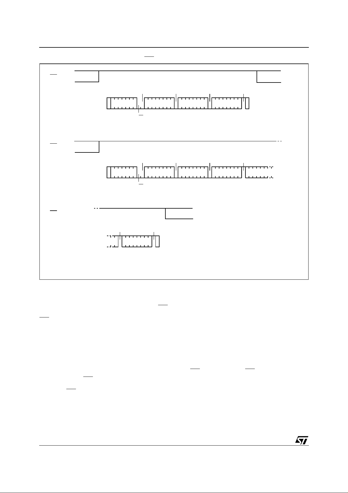
Figure 5. Wri te Mo de S e qu e nces with WC =1 (data wri te inhibi ted)
WC
ACK ACK ACK NO ACK
BYTE WRITE DEV SEL BYTE ADDR BYTE ADDR DATA IN
R/W
START
WC
ACK ACK ACK NO ACK
PAGE WRITE DEV SEL BYTE ADDR BYTE ADDR DATA IN 1
R/W
START
WC (cont'd)
NO ACK NO ACK
PAGE WRITE
(cont'd)
DATA IN N
STOP
STOP
DATA IN 2
AI01120C
sponds to each address byte with an acknowledge
bit, and then waits for the data byte.
Writing to the memory may be inhibited if the WC
input pin is taken high. Any write command with
WC
=1 (during a period of time from the START
condition until the end of the two address bytes)
will not modify the me mory c ontents, and t he ac-
not
companying data bytes will
be acknowledged,
as shown in Figure 5.
Byte Write
In the Byte Write mode, after the Device Select
Code and the address bytes, the master sends
one data byte. If the addressed lo cation is write
protected by the WC
pin, the memory replies with
a NoAck, and the location is not modified. If, instead, the WC
pin has been held at 0, as shown in
Figure 6, the memory replies with an Ack. The
master terminates the transfer by generating a
STOP condition.
6/20
Page Write
The Page Write mode allows u p to 64 by tes to be
written in a single write cycle, provided that they
are all located in the same ’row’ in the memory:
that is the most significant memory add ress bits
(b14-b6 for the M24256-A) are the same. If more
bytes are sent than will fit up to the end of the row,
a condition known as ‘roll-over’ occurs. Data starts
to become overwritten (in a way not formally specified in this data sheet).
The master sends from one up to 64 bytes of data,
each of which is acknow ledged by the memory if
the W C
pin is low. If the WC pin is high, the contents of the addressed memory location are not
modified, and each data byte is followed by a
NoAck. After each byte i s tran sferred, the i nte rnal
byte address counter (the 6 least significant bits
only) is incremented. The transfer is terminated by
the master generating a STOP condition.
When the master generates a STOP condition immediately after the Ack bit (in the “10
th
bit” time
 Loading...