

Ultra low drop-low noise BiCMOS 300 mA voltage
regulator for use with very low ESR output capacitor
Features
■ Input voltage from 2.5 V to 6 V
■ Stable with low ESR ceramic capacitors
■ Ultra low dropout voltage (150 mV typ. at 300
mA load, 0.4 mV typ. at 1 mA load)
■ Very low quiescent current (85 µA typ. at no
load, 200 µA typ. at 300 mA load; max 1.5 µA
in off mode)
■ Guaranteed output current up to 300 mA
■ Wide range of output voltage:
– from 1.25 V to 5.0 V
■ Fast turn-on time: typ. 240 µs
–[C
■ Logic-controlled electronic shutdown
■ Internal current and thermal limit
■ Output low noise voltage 30 µV
to 100 kHz
■ SVR of 55 dB at 1 kHz, 50 dB at 10 kHz
■ Temperature range: - 40 °C to 125 °C
Description
= 2.2 µF, C
O
= 33 nF and IO = 1 mA]
BYP
over 10 Hz
RMS
LDS3985xx
DFN6
makes it suitable for low power applications and in
battery powered systems. Regulator ground
current increases only slightly in dropout, further
prolonging the battery life. Shutdown logic control
function is available, this means that when the
device is used as local regulator, it is possible to
put a part of the board in standby, decreasing the
total power consumption. Typical applications are
in mobile phone and similar battery powered
wireless systems, portable information
appliances.
SOT23-5L
The LDS3985xx provides up to 300 mA, from 2.5
V to 6 V input voltage. It is stable with ceramic and
high quality tantalum capacitor. The ultra low drop
voltage, low quiescent current and low noise
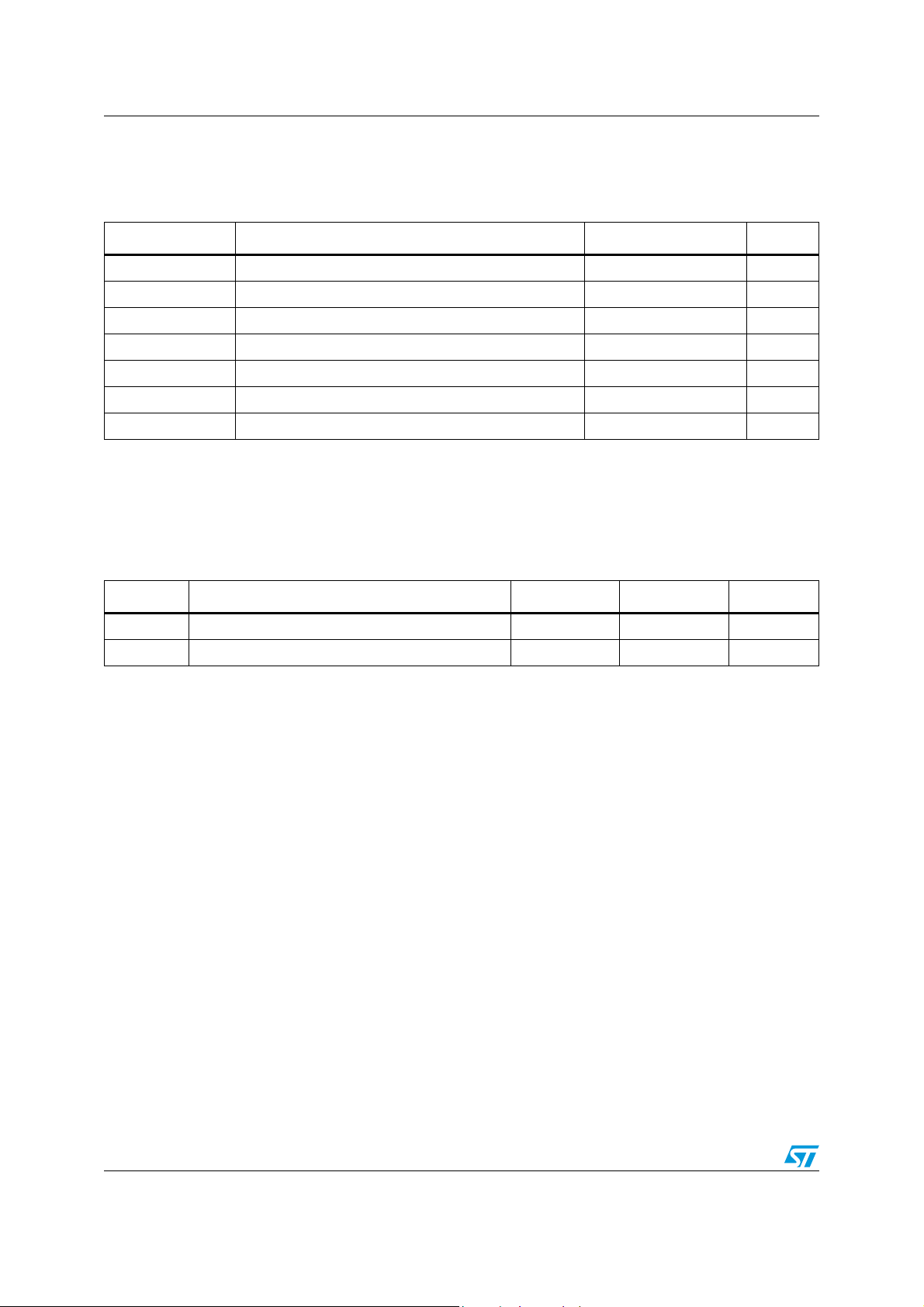
Table 1. Device summary
Part numbers Output voltages
LDS3985XX15 1.5 V
LDS3985XX18 1.8 V
LDS3985XX25 2.5 V
July 2010 Doc ID 11039 Rev 7 1/20
LDS3985XX28 2.8 V
LDS3985XX30 3.0 V
LDS3985XX33 3.3 V
LDS3985XX50 5.0 V
www.st.com
20

Contents LDS3985xx
Contents
1 Diagram . . . . . . . . . . . . . . . . . . . . . . . . . . . . . . . . . . . . . . . . . . . . . . . . . . . 3
2 Pin configuration . . . . . . . . . . . . . . . . . . . . . . . . . . . . . . . . . . . . . . . . . . . . 4
3 Typical application . . . . . . . . . . . . . . . . . . . . . . . . . . . . . . . . . . . . . . . . . . 5
4 Maximum ratings . . . . . . . . . . . . . . . . . . . . . . . . . . . . . . . . . . . . . . . . . . . . 6
5 Electrical characteristics . . . . . . . . . . . . . . . . . . . . . . . . . . . . . . . . . . . . . 7
6 Typical performance characteristics . . . . . . . . . . . . . . . . . . . . . . . . . . . . 9
7 Package mechanical data . . . . . . . . . . . . . . . . . . . . . . . . . . . . . . . . . . . . 12
8 Order codes . . . . . . . . . . . . . . . . . . . . . . . . . . . . . . . . . . . . . . . . . . . . . . 18
9 Revision history . . . . . . . . . . . . . . . . . . . . . . . . . . . . . . . . . . . . . . . . . . . 19
2/20 Doc ID 11039 Rev 7
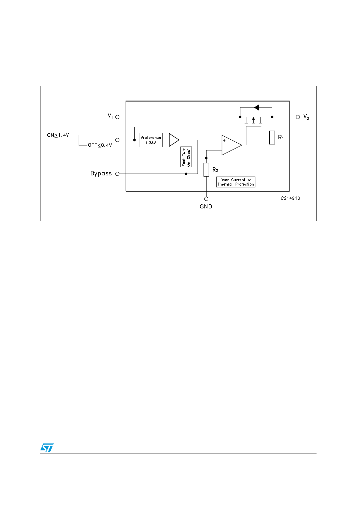
LDS3985xx Diagram
1 Diagram
Figure 1. Schematic diagram
Doc ID 11039 Rev 7 3/20
Pin configuration LDS3985xx
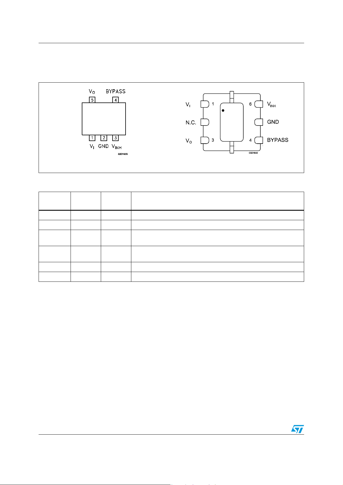
2 Pin configuration
Figure 2. Pin connections (top view for SOT23-5L, top through view for DFN6)
SOT23-5L
Table 2. Pin description
Pin n° for
SOT23-5L
11V
2 5 GND Common ground
36V
4 4 BYPASS
53V
- 2 N.C. Not connect
Pin n° for
DFN6
Symbol Name and function
Input voltage of the LDO
I
INH
Inhibit input voltage: on mode when V
0.4 V (Do not leave floating, not internally pulled down/up)
Bypass pin: connect an external capacitor (usually 10 nF) to minimize
noise voltage
Output voltage of the LDO
O
DFN6
≥ 1.2 V, off mode when V
INH
INH
≤
4/20 Doc ID 11039 Rev 7
LDS3985xx Typical application
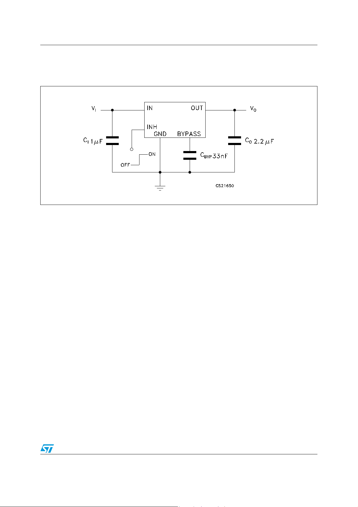
3 Typical application
Figure 3. Typical application circuit
Doc ID 11039 Rev 7 5/20
Maximum ratings LDS3985xx
4 Maximum ratings
Table 3. Absolute maximum ratings
Symbol Parameter Value Unit
(1)
V
V
T
V
P
STG
T
V
INH
I
O
OP
I
O
D
DC input voltage -0.3 to 6
DC output voltage -0.3 to VI+0.3 V
INHIBIT input voltage -0.3 to VI+0.3 V
Output current Internally limited
Power dissipation Internally limited
Storage temperature range -65 to 150 °C
Operating junction temperature range -40 to 125 °C
1. The input pin is able to withstand non repetitive spike of 6.5 V for 200 ms.
Note: Absolute maximum ratings are those values beyond which damage to the device may occur.
Functional operation under these condition is not implied.
Table 4. Thermal data
Symbol Parameter SOT23-5L DFN6 Unit
R
R
thJC
thJA
Thermal resistance junction-case 81 10 °C/W
Thermal resistance junction-ambient 255 55 °C/W
6/20 Doc ID 11039 Rev 7
 Loading...