

Ultra low drop-low noise BiCMOS 300 mA voltage
regulator for use with very low ESR output capacitor
Features
■ Input voltage from 2.5 V to 6 V
■ Stable with low ESR ceramic capacitors
■ Ultra low dropout voltage (150 mV typ. at 300
mA load, 0.4 mV typ. at 1 mA load)
■ Very low quiescent current (85 µA typ. at no
load, 200 µA typ. at 300 mA load; max 1.5 µA
in off mode)
■ Guaranteed output current up to 300 mA
■ Wide range of output voltage:
– from 1.25 V to 5.0 V
■ Fast turn-on time: typ. 240 µs
–[C
■ Logic-controlled electronic shutdown
■ Internal current and thermal limit
■ Output low noise voltage 30 µV
to 100 kHz
■ SVR of 55 dB at 1 kHz, 50 dB at 10 kHz
■ Temperature range: - 40 °C to 125 °C
Description
= 2.2 µF, C
O
= 33 nF and IO = 1 mA]
BYP
over 10 Hz
RMS
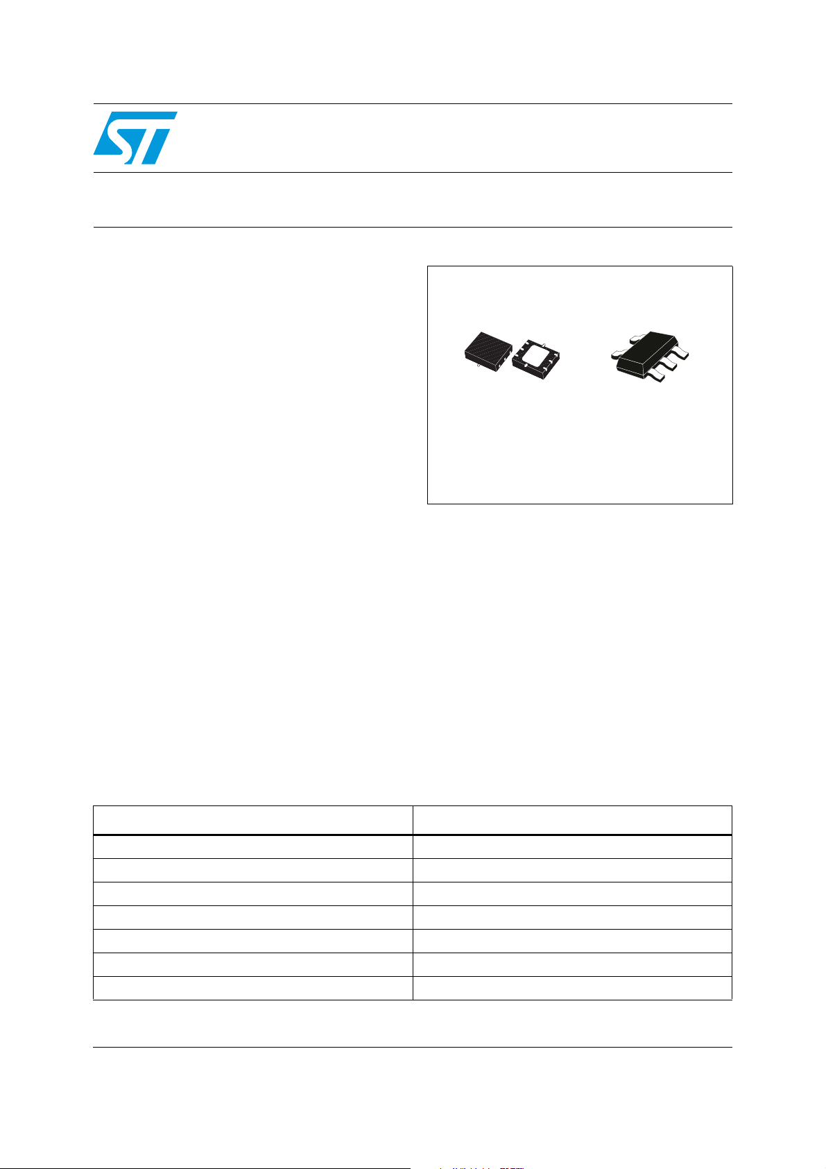
LDS3985xx
DFN6
makes it suitable for low power applications and in
battery powered systems. Regulator ground
current increases only slightly in dropout, further
prolonging the battery life. Shutdown logic control
function is available, this means that when the
device is used as local regulator, it is possible to
put a part of the board in standby, decreasing the
total power consumption. Typical applications are
in mobile phone and similar battery powered
wireless systems, portable information
appliances.
SOT23-5L
The LDS3985xx provides up to 300 mA, from 2.5
V to 6 V input voltage. It is stable with ceramic and
high quality tantalum capacitor. The ultra low drop
voltage, low quiescent current and low noise
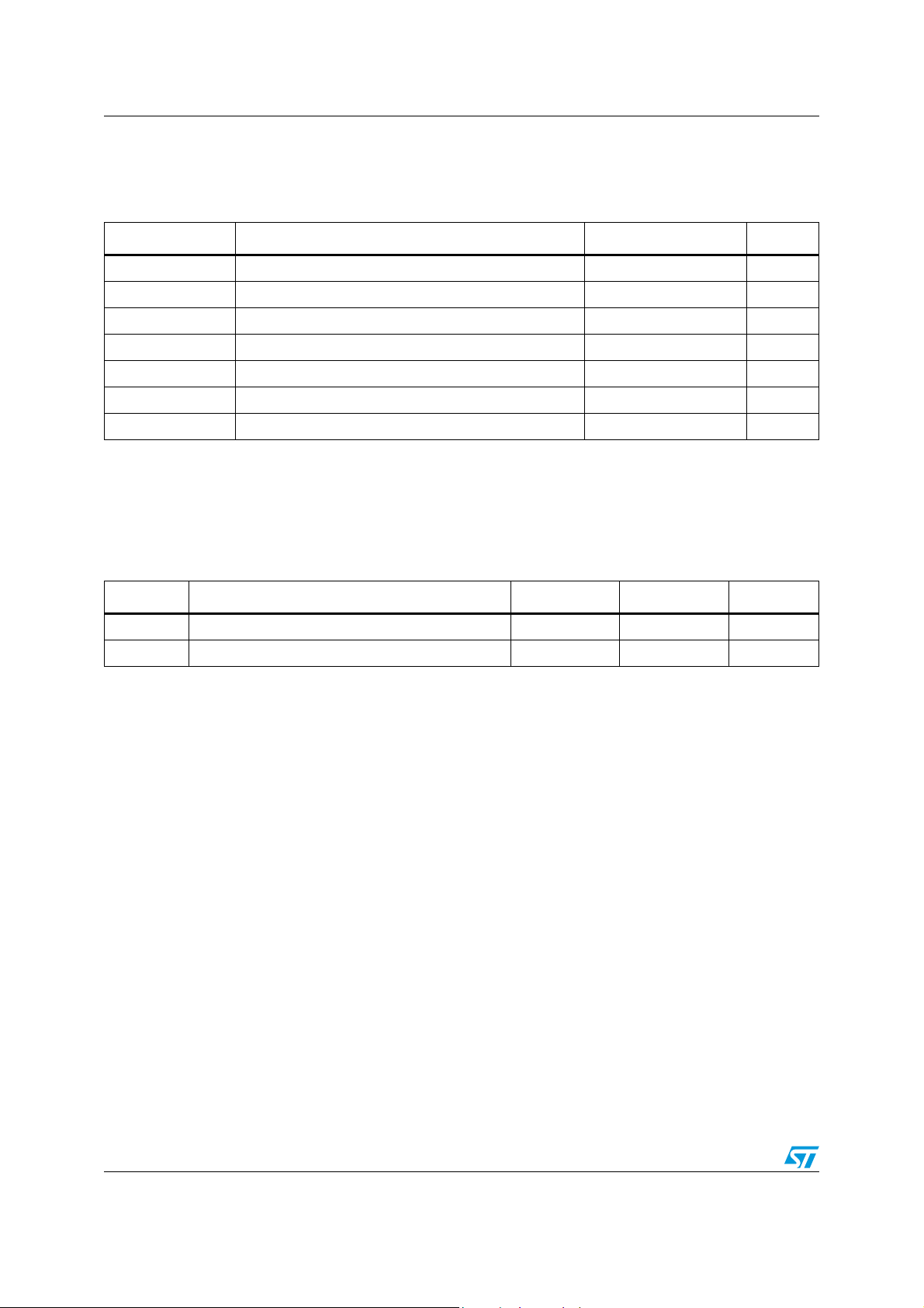
Table 1. Device summary
Part numbers Output voltages
LDS3985XX15 1.5 V
LDS3985XX18 1.8 V
LDS3985XX25 2.5 V
July 2010 Doc ID 11039 Rev 7 1/20
LDS3985XX28 2.8 V
LDS3985XX30 3.0 V
LDS3985XX33 3.3 V
LDS3985XX50 5.0 V
www.st.com
20

Contents LDS3985xx
Contents
1 Diagram . . . . . . . . . . . . . . . . . . . . . . . . . . . . . . . . . . . . . . . . . . . . . . . . . . . 3
2 Pin configuration . . . . . . . . . . . . . . . . . . . . . . . . . . . . . . . . . . . . . . . . . . . . 4
3 Typical application . . . . . . . . . . . . . . . . . . . . . . . . . . . . . . . . . . . . . . . . . . 5
4 Maximum ratings . . . . . . . . . . . . . . . . . . . . . . . . . . . . . . . . . . . . . . . . . . . . 6
5 Electrical characteristics . . . . . . . . . . . . . . . . . . . . . . . . . . . . . . . . . . . . . 7
6 Typical performance characteristics . . . . . . . . . . . . . . . . . . . . . . . . . . . . 9
7 Package mechanical data . . . . . . . . . . . . . . . . . . . . . . . . . . . . . . . . . . . . 12
8 Order codes . . . . . . . . . . . . . . . . . . . . . . . . . . . . . . . . . . . . . . . . . . . . . . 18
9 Revision history . . . . . . . . . . . . . . . . . . . . . . . . . . . . . . . . . . . . . . . . . . . 19
2/20 Doc ID 11039 Rev 7
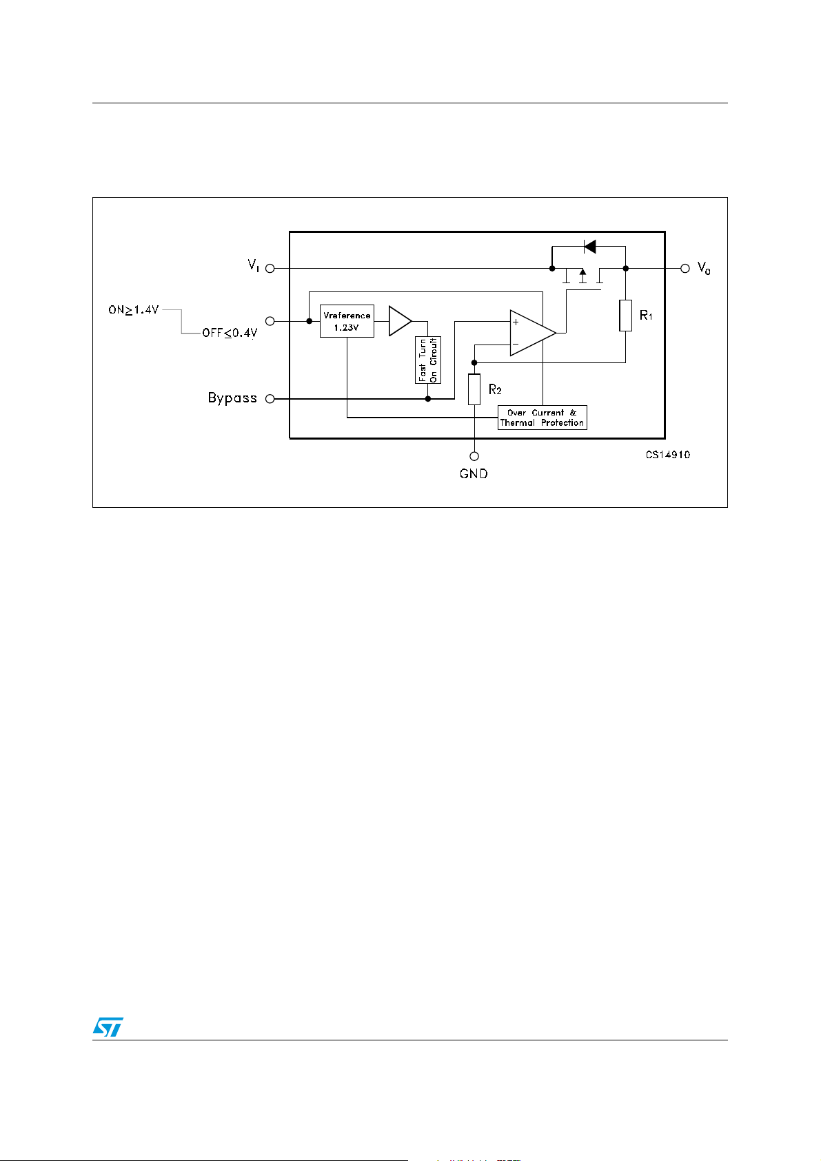
LDS3985xx Diagram
1 Diagram
Figure 1. Schematic diagram
Doc ID 11039 Rev 7 3/20
Pin configuration LDS3985xx
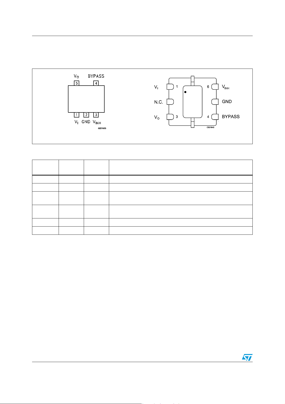
2 Pin configuration
Figure 2. Pin connections (top view for SOT23-5L, top through view for DFN6)
SOT23-5L
Table 2. Pin description
Pin n° for
SOT23-5L
11V
2 5 GND Common ground
36V
4 4 BYPASS
53V
- 2 N.C. Not connect
Pin n° for
DFN6
Symbol Name and function
Input voltage of the LDO
I
INH
Inhibit input voltage: on mode when V
0.4 V (Do not leave floating, not internally pulled down/up)
Bypass pin: connect an external capacitor (usually 10 nF) to minimize
noise voltage
Output voltage of the LDO
O
DFN6
≥ 1.2 V, off mode when V
INH
INH
≤
4/20 Doc ID 11039 Rev 7
LDS3985xx Typical application
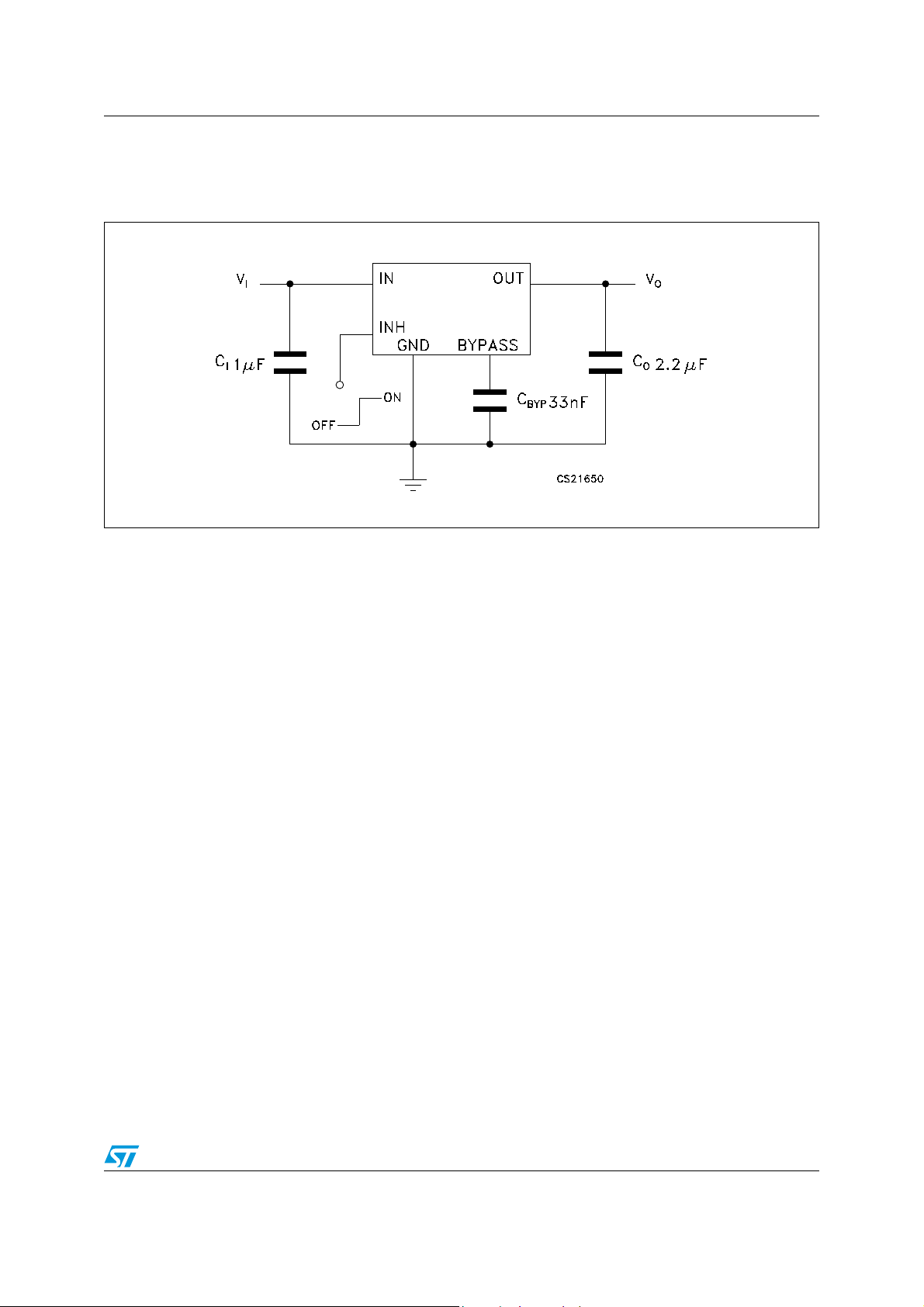
3 Typical application
Figure 3. Typical application circuit
Doc ID 11039 Rev 7 5/20
Maximum ratings LDS3985xx
4 Maximum ratings
Table 3. Absolute maximum ratings
Symbol Parameter Value Unit
(1)
V
V
T
V
P
STG
T
V
INH
I
O
OP
I
O
D
DC input voltage -0.3 to 6
DC output voltage -0.3 to VI+0.3 V
INHIBIT input voltage -0.3 to VI+0.3 V
Output current Internally limited
Power dissipation Internally limited
Storage temperature range -65 to 150 °C
Operating junction temperature range -40 to 125 °C
1. The input pin is able to withstand non repetitive spike of 6.5 V for 200 ms.
Note: Absolute maximum ratings are those values beyond which damage to the device may occur.
Functional operation under these condition is not implied.
Table 4. Thermal data
Symbol Parameter SOT23-5L DFN6 Unit
R
R
thJC
thJA
Thermal resistance junction-case 81 10 °C/W
Thermal resistance junction-ambient 255 55 °C/W
6/20 Doc ID 11039 Rev 7

LDS3985xx Electrical characteristics
5 Electrical characteristics
TJ = 25 °C, VI = V
V
= 1.4 V, unless otherwise specified.
INH
Table 5. Electrical characteristics for LDS3985xx
O(NOM)
+ 0.5 V, CI = 1 µF, CO = 2.2 µF, C
= 33 nF, IO = 1 mA,
BYP
Symbol Parameter Test conditions Min. Typ. Max. Unit
V
Operating input voltage 2.5 6 V
I
I
= 1 mA -50 50
O
= - 40 to 125 °C -75 75
T
J
I
= 1 mA -2 2
O
TJ= - 40 to 125 °C -3 3
VI = V
TJ = - 40 to 125 °C
= 4.7 to 5 V -0.19 0.19
V
O
= 1 mA to 300 mA, VO ≤ 2.5 V
I
O
TJ = - 40 to 125 °C
I
= 1 mA to 300 mA, VO ≥ 2.5 V
O
TJ = - 40 to 125 °C
VI = V
= tF = 30 µs
t
R
I
= 0 85
O
= 0, TJ = - 40 to 125 °C 150
I
O
I
= 0 to 300 mA 200
O
= 0 to 300 mA, TJ = - 40 to 125 °C 300
I
O
+ 0.5 to 6 V,
O(NOM)
+ 1 V, IO = 300 mA,
O(NOM)
-0.1 0.1
0.005 0.01 %/mA
0.0008 0.004 %/mA
5mV
ΔV
ΔV
ΔV
ΔV
V
Output voltage < 2.5 V
O
V
Output voltage ≥ 2.5 V
O
Line regulation
O
Load regulation
O
Load regulation
O
Output AC line regulation
(2)
O
Quiescent current
ON MODE: V
I
Q
(1)
INH
= 1.24 V
0.003
OFF MODE: V
INH
= 0.4 V
T
= - 40 to 125 °C 1.5
J
IO = 1 mA 0.4
= 1 mA, TJ = -40 to 125 °C 2
I
O
I
= 150 mA 60
V
DROP
SVR Supply voltage rejection
Dropout voltage
Short circuit current RL = 0 600 mA
I
SC
(3)
O
= 150 mA, TJ = - 40 to 125 °C 100
I
O
= 300 mA 150
I
O
I
= 300 mA, TJ = - 40 to 125 °C 250
O
= V
V
I
O(NOM)
V
For V
= 0.1 V, IO = 50 mA
RIPPLE
O(NOM)
VI = 2.55 V
+0.25 V ±
< 2.5 V,
f = 1 kHz 55
f = 10 kHz 50
mV
% of
V
O(NOM)
%/V
µA
mV
dB
PP
I
O(PK)
Peak output current VO ≥ V
- 5 % 300 550 mA
O(NOM)
Doc ID 11039 Rev 7 7/20

Electrical characteristics LDS3985xx
Table 5. Electrical characteristics for LDS3985xx (continued)
Symbol Parameter Test conditions Min. Typ. Max. Unit
V
INH
Inhibit input logic High 1.4
I
Inhibit input current V
INH
eN Output noise voltage B
Inhibit input logic Low
t
T
SHDN
Turn On time
ON
Thermal shutdown
(4)
= 2.5 V to 6 V, TJ= - 40 to 125 °C
V
I
= 0.4 V, VI = 6 V ±1 nA
INH
= 10 Hz to 100 kHz, CO = 2.2 µF 30 µV
W
C
= 33 nF 240 µs
BYP
(5)
160 °C
0.4
V
RMS
Capacitance 2.2 22 µF
C
Output capacitor
O
1. For V
2. For V
3. Dropout voltage is the input-to-output voltage difference at which the output voltage is 100 mV below its nominal value. This
specification does not apply for input voltages below 2.5 V
4. Turn-on time is time measured between the enable input just exceeding V
reaching 95 % of its nominal value
< 2 V, VI = 2.5 V
O(NOM)
= 1.25 V, VI = 2.5 V
O(NOM)
5. Typical thermal protection hysteresis is 20 °C
ESR 5 5000 mΩ
high value and the output voltage just
INH
8/20 Doc ID 11039 Rev 7

LDS3985xx Typical performance characteristics
6 Typical performance characteristics
TJ = 25 °C, VI = V
V
= 1.4 V, unless otherwise specified.
INH
Figure 4. Output voltage vs. temp. (V
O(NOM)
+ 0.5 V, CI = 1 µF, CO = 2.2 µF, C
= 2.5 V) Figure 5. Output voltage vs. temp. (VI = 3.2 V)
I
= 33 nF, IO = 1 mA,
BYP
Figure 6. Output voltage vs. temp. (VI = 3.8 V) Figure 7. Shutdown voltage vs. temperature
(V
= 1.35 V)
O
Figure 8. Shutdown voltage vs. temperature
(V
= 3.3 V)
O
Figure 9. Line regulation vs. temperature
(VI = 2.5 V to 6 V)
Doc ID 11039 Rev 7 9/20

Typical performance characteristics LDS3985xx
Figure 10. Line regulation vs. temperature
(V
= 3.2 V to 6 V)
I
Figure 12. Quiescent current vs. temperature
(V
= 2.5 V)
I
Figure 11. Line regulation vs. temperature
(VI = 3.8 V to 6 V)
Figure 13. Quiescent current vs. temperature
(VI = 6 V)
Figure 14. Quiescent current vs. temperature
(V
= 3.4 V)
10/20 Doc ID 11039 Rev 7
I
Figure 15. Supply voltage rejection vs.
frequency

LDS3985xx Typical performance characteristics
Figure 16. Dropout voltage vs. temperature Figure 17. Dropout voltage vs. output current
Figure 18. Inhibit transient
VI = 5 V, IO = 1 mA, V
C
= 10 nF, TR = TF = 1 µs
BYP
INH
= 0 to 1.2 V, CI = CO = 1 µF (cer),
Doc ID 11039 Rev 7 11/20

Package mechanical data LDS3985xx
7 Package mechanical data
In order to meet environmental requirements, ST offers these devices in different grades of
ECOPACK
specifications, grade definitions and product status are available at: www.st.com.
ECOPACK
®
packages, depending on their level of environmental compliance. ECOPACK®
®
is an ST trademark.
12/20 Doc ID 11039 Rev 7

LDS3985xx Package mechanical data
SOT23-5L mechanical data
mm. mils.
Dim.
Min. Typ. Max. Min. Typ. Max.
A0.90 1.45 35.4 57.1
A1 0.00 0.10 0.0 3.9
A2 0.901.30 35.4 51.2
b 0.35 0.50 13.7 19.7
C0.09 0.20 3.5 7.8
D2.80 3.00 110.2 118.1
E 1.50 1.75 59.0 68.8
e0.95 37.4
H 2.60 3.00 102.3 118.1
L 0.10 0.60 3.9 23.6
7049676D
Doc ID 11039 Rev 7 13/20

Package mechanical data LDS3985xx
DFN6 (3x3 mm) mechanical data
mm. inch.
Dim.
Min. Typ. Max. Min. Typ. Max.
A0.800.90 1.00 0.031 0.035 0.039
A1 0 0.02 0.05 0 0.001 0.002
A3 0.20 0.008
b 0.23 0.300.38 0.009 0.012 0.015
D2.90 3.00 3.10 0.114 0.118 0.122
D2 2.23 2.38 2.48 0.088 0.094 0.098
E2.90 3.00 3.10 0.114 0.118 0.122
E2 1.50 1.65 1.75 0.059 0.065 0.069
e0.950.037
L0.30 0.40 0.50 0.012 0.016 0.020
14/20 Doc ID 11039 Rev 7
7946637A

LDS3985xx Package mechanical data
DFN6D (3x3 mm) mechanical data
mm. inch.
Dim.
Min. Typ. Max. Min. Typ. Max.
A0.80 1.00 0.031 0.039
A1 0 0.02 0.05 0 0.001 0.002
A3 0.20 0.008
b 0.23 0.45 0.009 0.018
D2.90 3.00 3.10 0.114 0.118 0.122
D2 2.23 2.50 0.088 0.098
E2.90 3.00 3.10 0.114 0.118 0.122
E2 1.50 1.75 0.059 0.069
e0.950.037
L0.30 0.40 0.50 0.012 0.016 0.020
7946637B
Doc ID 11039 Rev 7 15/20

Package mechanical data LDS3985xx
Tape & reel SOT23-xL mechanical data
Dim.
mm. inch.
Min. Typ. Max. Min. Typ. Max.
A180 7.086
C 12.8 13.0 13.2 0.504 0.512 0.519
D 20.2 0.795
N60 2.362
T 14.4 0.567
Ao 3.133.233.33 0.123 0.127 0.131
Bo 3.07 3.17 3.27 0.120 0.124 0.128
Ko 1.27 1.37 1.47 0.050 0.054 0.0.58
Po 3.9 4.0 4.1 0.153 0.157 0.161
P 3.9 4.0 4.1 0.153 0.157 0.161
16/20 Doc ID 11039 Rev 7

LDS3985xx Package mechanical data
Tape & reel QFNxx/DFNxx (3x3) mechanical data
mm. inch.
Dim.
Min. Typ. Max. Min. Typ. Max.
A180 7.087
C 12.8 13.2 0.504 0.519
D 20.2 0.795
N60 2.362
T 14.4 0.567
Ao 3.3 0.130
Bo 3.3 0.130
Ko 1.1 0.043
Po 4 0.157
P 8 0.315
Doc ID 11039 Rev 7 17/20

Order codes LDS3985xx
8 Order codes
Table 6. Order codes
Packages
Output voltage
SOT23-5L DFN6 DFN6D
LDS3985M125R
LDS3985M135R
(1)
(1)
LDS3985PM12R
LDS3985PM13R
LDS3985M15R LDS3985PM15R
LDS3985M18R LDS3985PM18R
LDS3985M20R
LDS3985M21R
LDS3985M22R
(1)
(1)
(1)
LDS3985PM20R
LDS3985PM21R
LDS3985PM22R
LDS3985M25R LDS3985PM25R
LDS3985M26R
LDS3985M27R
(1)
(1)
LDS3985PM26R
LDS3985PM27R
(1)
(1)
(1)
(1)
(1)
(1)
(1)
(1)
(1)
(1)
1.25 V
1.35 V
LDS3985PU15R 1.5 V
1.8 V
2.0 V
2.1 V
2.2 V
2.5 V
2.6 V
2.7 V
LDS3985M28R LDS3985PU28R 2.8 V
(1)
(1)
LDS3985PM285R
LDS3985PM29R
LDS3985M285R
LDS3985M29R
LDS3985M30R LDS3985PM30R
(1)
(1)
(1)
LDS3985M33R LDS3985PU33R 3.3 V
LDS3985M47R
LDS3985M48R
LDS3985M49R
(1)
(1)
(1)
LDS3985PM47R
LDS3985PM48R
LDS3985PM49R
LDS3985M50R LDS3985PM50R
1. Available on request.
(1)
(1)
(1)
(1)
2.85 V
2.9 V
3.0 V
4.7 V
4.8 V
4.9 V
5.0 V
18/20 Doc ID 11039 Rev 7

LDS3985xx Revision history
9 Revision history
Table 7. Document revision history
Date Revision Changes
02-Dec-2004 1 First release.
10-Apr-2007 2 Added: new package TSOT23-5L.
16-May-2007 3 Added: new mechanical data DFN6D and order codes updated.
06-Sep-2007 4 Added: Ta b le 1 in cover page.
11-Jun-2008 5 Modified: Table 6 on page 18.
11-Jul-2009 6 Modified: Table 6 on page 18.
29-Jul-2010 7 Modified: Table 1 on page 1 and Table 6 on page 18.
Doc ID 11039 Rev 7 19/20

LDS3985xx
Please Read Carefully:
Information in this document is provided solely in connection with ST products. STMicroelectronics NV and its subsidiaries (“ST”) reserve the
right to make changes, corrections, modifications or improvements, to this document, and the products and services described herein at any
time, without notice.
All ST products are sold pursuant to ST’s terms and conditions of sale.
Purchasers are solely responsible for the choice, selection and use of the ST products and services described herein, and ST assumes no
liability whatsoever relating to the choice, selection or use of the ST products and services described herein.
No license, express or implied, by estoppel or otherwise, to any intellectual property rights is granted under this document. If any part of this
document refers to any third party products or services it shall not be deemed a license grant by ST for the use of such third party products
or services, or any intellectual property contained therein or considered as a warranty covering the use in any manner whatsoever of such
third party products or services or any intellectual property contained therein.
UNLESS OTHERWISE SET FORTH IN ST’S TERMS AND CONDITIONS OF SALE ST DISCLAIMS ANY EXPRESS OR IMPLIED
WARRANTY WITH RESPECT TO THE USE AND/OR SALE OF ST PRODUCTS INCLUDING WITHOUT LIMITATION IMPLIED
WARRANTIES OF MERCHANTABILITY, FITNESS FOR A PARTICULAR PURPOSE (AND THEIR EQUIVALENTS UNDER THE LAWS
OF ANY JURISDICTION), OR INFRINGEMENT OF ANY PATENT, COPYRIGHT OR OTHER INTELLECTUAL PROPERTY RIGHT.
UNLESS EXPRESSLY APPROVED IN WRITING BY AN AUTHORIZED ST REPRESENTATIVE, ST PRODUCTS ARE NOT
RECOMMENDED, AUTHORIZED OR WARRANTED FOR USE IN MILITARY, AIR CRAFT, SPACE, LIFE SAVING, OR LIFE SUSTAINING
APPLICATIONS, NOR IN PRODUCTS OR SYSTEMS WHERE FAILURE OR MALFUNCTION MAY RESULT IN PERSONAL INJURY,
DEATH, OR SEVERE PROPERTY OR ENVIRONMENTAL DAMAGE. ST PRODUCTS WHICH ARE NOT SPECIFIED AS "AUTOMOTIVE
GRADE" MAY ONLY BE USED IN AUTOMOTIVE APPLICATIONS AT USER’S OWN RISK.
Resale of ST products with provisions different from the statements and/or technical features set forth in this document shall immediately void
any warranty granted by ST for the ST product or service described herein and shall not create or extend in any manner whatsoever, any
liability of ST.
ST and the ST logo are trademarks or registered trademarks of ST in various countries.
Information in this document supersedes and replaces all information previously supplied.
The ST logo is a registered trademark of STMicroelectronics. All other names are the property of their respective owners.
© 2010 STMicroelectronics - All rights reserved
Australia - Belgium - Brazil - Canada - China - Czech Republic - Finland - France - Germany - Hong Kong - India - Israel - Italy - Japan -
STMicroelectronics group of companies
Malaysia - Malta - Morocco - Philippines - Singapore - Spain - Sweden - Switzerland - United Kingdom - United States of America
www.st.com
20/20 Doc ID 11039 Rev 7
 Loading...