

LD49150XX10, LD49150XX12
1.5 A very low drop for low output voltage regulator
Features
■ Input voltage range:
–V
= 1.4 V to 5.5 V
I
–V
■ Stable with ceramic capacitor
■ ±1.5 % initial tolerance
■ Maximum dropout voltage (V
over temperature
■ Adjustable output voltage down to 0.8 V
■ Ultra fast transient response (up to 10 MHz
bandwidth)
■ Excellent line and load regulation
specifications
■ Logic controlled shutdown option
■ Thermal shutdown and current limit protection
■ Junction temperature range: - 25 °C to 125 °C
Applications
■ Graphics processors
■ PC add-in cards
■ Microprocessor core voltage supply
■ Low voltage digital ICs
■ High efficiency linear power supplies
■ SMPS post regulators
= 3 V to 6 V
BIAS
- VO) of 200 mV
I
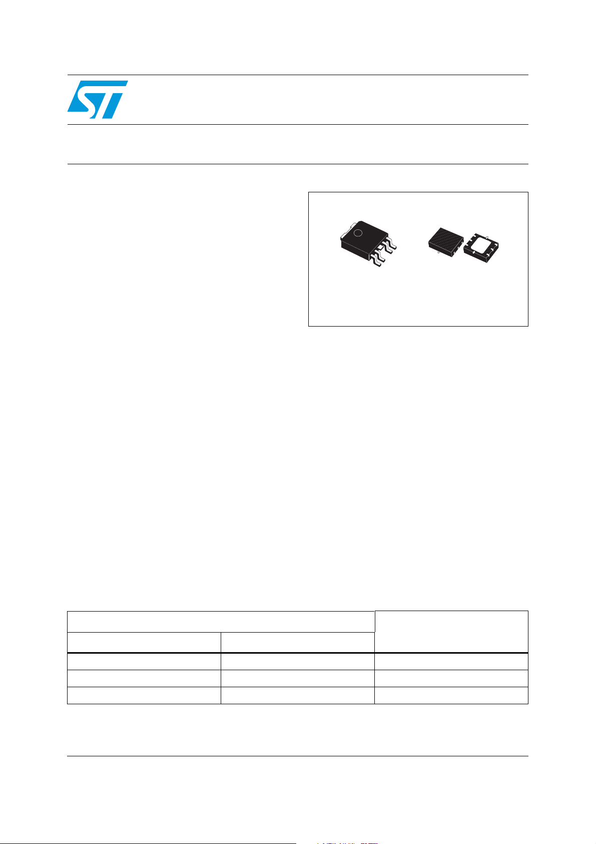
LD49150XX08
PPAK
Description
The LD49150xx is a high-bandwidth, low-dropout,
1.5 A voltage regulator, ideal for powering core
voltages of low-power microprocessors. The
LD49150xx implements a dual supply
configuration allowing for very low output
impedance and very fast transient response. The
LD49150xx requires a bias input supply and a
main input supply, allowing for ultra-low input
voltages on the main supply rail. The input supply
operates from 1.4 V to 5.5 V and the bias supply
requires between 3 V and 6 V for proper
operation. The LD49150xx offers fixed output
voltages from 0.8 V to 1.8 V and adjustable output
voltages down to 0.8 V. The LD49150xx requires a
minimum output capacitance for stability, and
work optimally with small ceramic capacitors.
DFN6 (3x3 mm)
Table 1. Device summary
Order codes
PPAK (tape and reel) DFN6 (tape and reel)
LD49150PT08R 0.8 V
LD49150PT10R LD49150PU10R 1.0 V
LD49150PT12R LD49150PU12R 1.2 V
1. Available on request.
2. Adjustable version.
June 2010 Doc ID 13446 Rev 3 1/22
(1)
Output voltages
(2)
www.st.com
22

Contents LD49150XX08, LD49150XX10, LD49150XX12
Contents
1 Typical application circuits . . . . . . . . . . . . . . . . . . . . . . . . . . . . . . . . . . . 3
2 Alternative application circuits . . . . . . . . . . . . . . . . . . . . . . . . . . . . . . . . 4
3 Pin configuration . . . . . . . . . . . . . . . . . . . . . . . . . . . . . . . . . . . . . . . . . . . 5
4 Diagram . . . . . . . . . . . . . . . . . . . . . . . . . . . . . . . . . . . . . . . . . . . . . . . . . . . 6
5 Maximum ratings . . . . . . . . . . . . . . . . . . . . . . . . . . . . . . . . . . . . . . . . . . . . 7
6 Electrical characteristics . . . . . . . . . . . . . . . . . . . . . . . . . . . . . . . . . . . . . 8
7 Typical characteristics . . . . . . . . . . . . . . . . . . . . . . . . . . . . . . . . . . . . . . . 9
8 Application hints . . . . . . . . . . . . . . . . . . . . . . . . . . . . . . . . . . . . . . . . . . . 13
8.1 Input supply voltage (VIN) . . . . . . . . . . . . . . . . . . . . . . . . . . . . . . . . . . . . . 13
8.2 Bias supply voltage (V
8.3 External capacitors . . . . . . . . . . . . . . . . . . . . . . . . . . . . . . . . . . . . . . . . . . 13
8.4 Output capacitor . . . . . . . . . . . . . . . . . . . . . . . . . . . . . . . . . . . . . . . . . . . . 13
8.5 Minimum load current . . . . . . . . . . . . . . . . . . . . . . . . . . . . . . . . . . . . . . . . 13
8.6 Power sequencing recommendations . . . . . . . . . . . . . . . . . . . . . . . . . . . 14
8.7 Power dissipation/heatsinking . . . . . . . . . . . . . . . . . . . . . . . . . . . . . . . . . 14
8.8 Heatsinking PPAK package . . . . . . . . . . . . . . . . . . . . . . . . . . . . . . . . . . . 15
8.9 Adjustable regulator design . . . . . . . . . . . . . . . . . . . . . . . . . . . . . . . . . . . 15
8.10 Enable . . . . . . . . . . . . . . . . . . . . . . . . . . . . . . . . . . . . . . . . . . . . . . . . . . . 15
) . . . . . . . . . . . . . . . . . . . . . . . . . . . . . . . . . . . 13
BIAS
9 Package mechanical data . . . . . . . . . . . . . . . . . . . . . . . . . . . . . . . . . . . . 16
10 Revision history . . . . . . . . . . . . . . . . . . . . . . . . . . . . . . . . . . . . . . . . . . . 21
2/22 Doc ID 13446 Rev 3
LD49150XX08, LD49150XX10, LD49150XX12 Typical application circuits
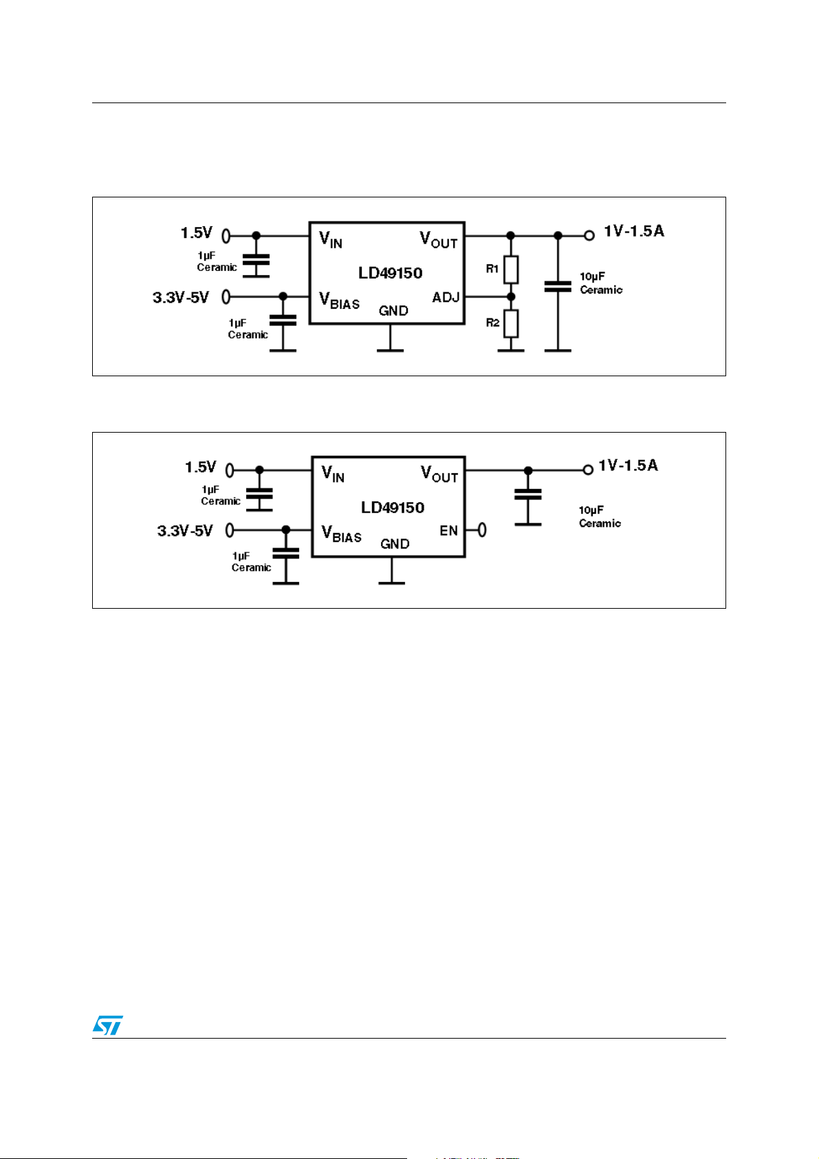
1 Typical application circuits
Figure 1. Adjustable version
Figure 2. Fixed version with Enable
Doc ID 13446 Rev 3 3/22
Alternative application circuits LD49150XX08, LD49150XX10, LD49150XX12
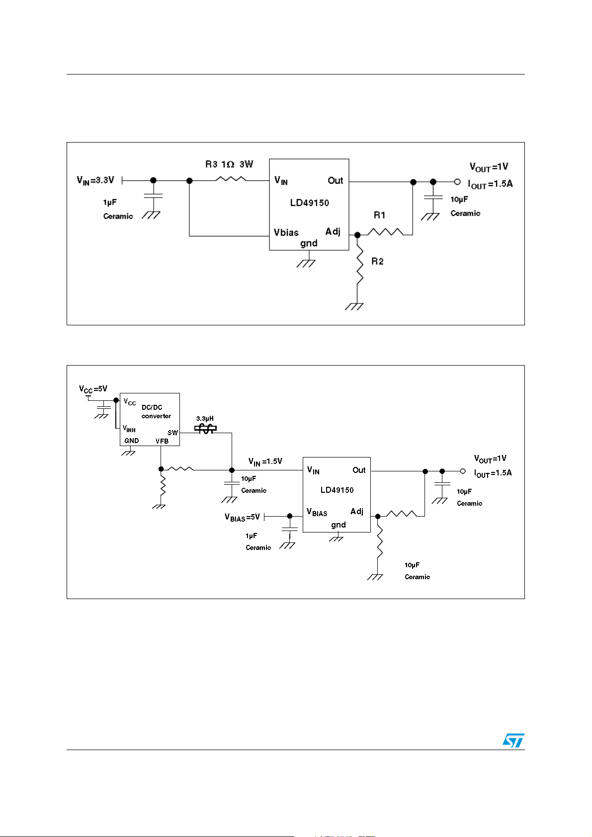
2 Alternative application circuits
Figure 3. Single supply voltage solution
Figure 4. LD49150xx plus DC-DC pre-regulator to reduce power dissipation
4/22 Doc ID 13446 Rev 3
LD49150XX08, LD49150XX10, LD49150XX12 Pin configuration
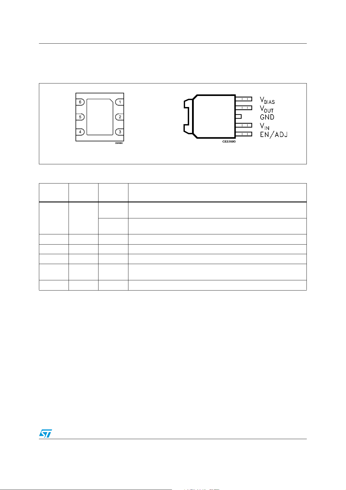
3 Pin configuration
Figure 5. Pin connections (top view for PPAK, bottom view for DFN)
DFN6 (3 x 3 mm)
Table 2. Pin description
Pin n° for
PPAK
12
23V
3 1 GND Ground (TAB is connected to ground).
44V
56V
Pin n° for
DFN
Symbol Note
EN
ADJ
OUT
BIAS
For fixed versions: Enable (Input) - Logic High = Enable, Logic Low =
Shutdown.
For adjustable versions: Adjustable regulator feedback input. Connect to
resistor voltage divider.
Input voltage which supplies current to the output power device.
IN
Regulator output.
Input bias voltage for powering all circuitry on the regulator with the
exception of the output power device.
5 N.C. Not connect.
PPAK
Doc ID 13446 Rev 3 5/22
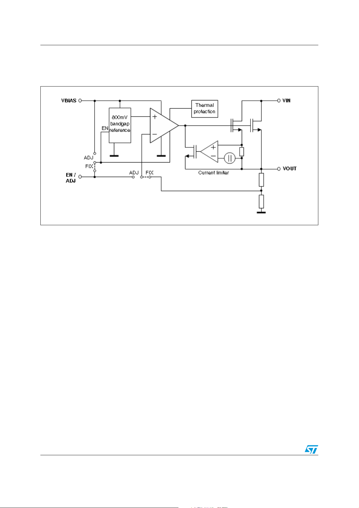
Diagram LD49150XX08, LD49150XX10, LD49150XX12
4 Diagram
Figure 6. Block diagram
6/22 Doc ID 13446 Rev 3
LD49150XX08, LD49150XX10, LD49150XX12 Maximum ratings
5 Maximum ratings
Table 3. Absolute maximum ratings
(1)
Symbol Parameter Value Unit
V
IN
V
OUT
V
BIAS
V
EN
P
D
T
STG
1. All the values are referred to ground.
Supply voltage -0.3 to 7 V
Output voltage
-0.3 to V
-0.3 to V
IN
BIAS
+ 0.3
+ 0.3
V
BIAS supply voltage -0.3 to 7 V
Enable input voltage -0.3 to 7 V
Power dissipation Internally limited
Storage temperature range -50 to 150 °C
Note: Absolute maximum ratings are those values beyond which damage to the device may occur.
Functional operation under these conditions is not implied.
Table 4. Operating ratings
Symbol Parameter Value Unit
V
V
V
OUT
BIAS
V
EN
T
IN
J
Supply voltage 1.4 to 5.5 V
Output voltage 0.8 to 4.5 V
BIAS supply voltage 3 to 6 V
Enable input voltage 0 to V
BIAS
V
Junction temperature range -25 to 125 °C
Doc ID 13446 Rev 3 7/22
 Loading...