

LD49150XX10, LD49150XX12
1.5 A very low drop for low output voltage regulator
Features
■ Input voltage range:
–V
= 1.4 V to 5.5 V
I
–V
■ Stable with ceramic capacitor
■ ±1.5 % initial tolerance
■ Maximum dropout voltage (V
over temperature
■ Adjustable output voltage down to 0.8 V
■ Ultra fast transient response (up to 10 MHz
bandwidth)
■ Excellent line and load regulation
specifications
■ Logic controlled shutdown option
■ Thermal shutdown and current limit protection
■ Junction temperature range: - 25 °C to 125 °C
Applications
■ Graphics processors
■ PC add-in cards
■ Microprocessor core voltage supply
■ Low voltage digital ICs
■ High efficiency linear power supplies
■ SMPS post regulators
= 3 V to 6 V
BIAS
- VO) of 200 mV
I
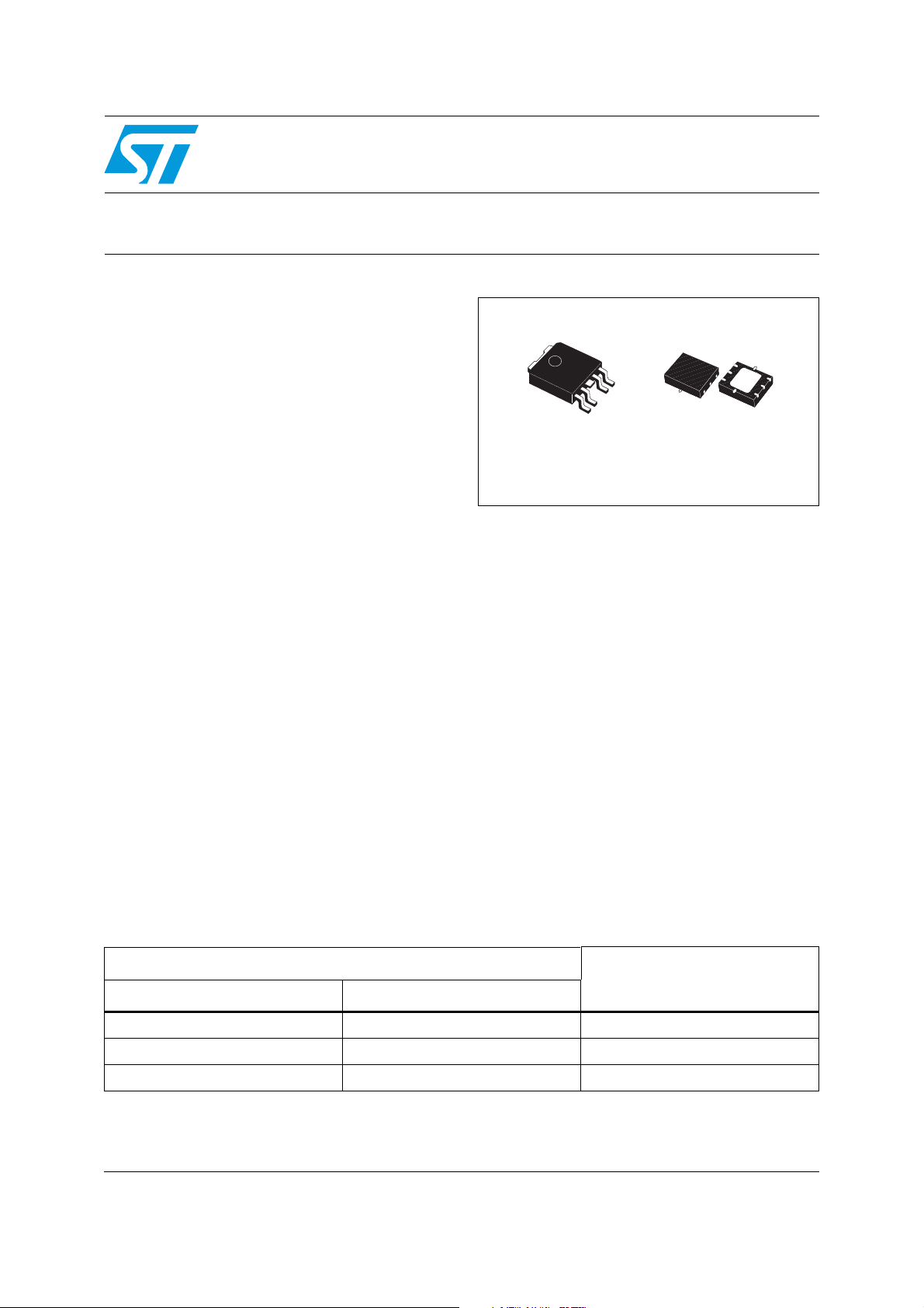
LD49150XX08
PPAK
Description
The LD49150xx is a high-bandwidth, low-dropout,
1.5 A voltage regulator, ideal for powering core
voltages of low-power microprocessors. The
LD49150xx implements a dual supply
configuration allowing for very low output
impedance and very fast transient response. The
LD49150xx requires a bias input supply and a
main input supply, allowing for ultra-low input
voltages on the main supply rail. The input supply
operates from 1.4 V to 5.5 V and the bias supply
requires between 3 V and 6 V for proper
operation. The LD49150xx offers fixed output
voltages from 0.8 V to 1.8 V and adjustable output
voltages down to 0.8 V. The LD49150xx requires a
minimum output capacitance for stability, and
work optimally with small ceramic capacitors.
DFN6 (3x3 mm)
Table 1. Device summary
Order codes
PPAK (tape and reel) DFN6 (tape and reel)
LD49150PT08R 0.8 V
LD49150PT10R LD49150PU10R 1.0 V
LD49150PT12R LD49150PU12R 1.2 V
1. Available on request.
2. Adjustable version.
June 2010 Doc ID 13446 Rev 3 1/22
(1)
Output voltages
(2)
www.st.com
22

Contents LD49150XX08, LD49150XX10, LD49150XX12
Contents
1 Typical application circuits . . . . . . . . . . . . . . . . . . . . . . . . . . . . . . . . . . . 3
2 Alternative application circuits . . . . . . . . . . . . . . . . . . . . . . . . . . . . . . . . 4
3 Pin configuration . . . . . . . . . . . . . . . . . . . . . . . . . . . . . . . . . . . . . . . . . . . 5
4 Diagram . . . . . . . . . . . . . . . . . . . . . . . . . . . . . . . . . . . . . . . . . . . . . . . . . . . 6
5 Maximum ratings . . . . . . . . . . . . . . . . . . . . . . . . . . . . . . . . . . . . . . . . . . . . 7
6 Electrical characteristics . . . . . . . . . . . . . . . . . . . . . . . . . . . . . . . . . . . . . 8
7 Typical characteristics . . . . . . . . . . . . . . . . . . . . . . . . . . . . . . . . . . . . . . . 9
8 Application hints . . . . . . . . . . . . . . . . . . . . . . . . . . . . . . . . . . . . . . . . . . . 13
8.1 Input supply voltage (VIN) . . . . . . . . . . . . . . . . . . . . . . . . . . . . . . . . . . . . . 13
8.2 Bias supply voltage (V
8.3 External capacitors . . . . . . . . . . . . . . . . . . . . . . . . . . . . . . . . . . . . . . . . . . 13
8.4 Output capacitor . . . . . . . . . . . . . . . . . . . . . . . . . . . . . . . . . . . . . . . . . . . . 13
8.5 Minimum load current . . . . . . . . . . . . . . . . . . . . . . . . . . . . . . . . . . . . . . . . 13
8.6 Power sequencing recommendations . . . . . . . . . . . . . . . . . . . . . . . . . . . 14
8.7 Power dissipation/heatsinking . . . . . . . . . . . . . . . . . . . . . . . . . . . . . . . . . 14
8.8 Heatsinking PPAK package . . . . . . . . . . . . . . . . . . . . . . . . . . . . . . . . . . . 15
8.9 Adjustable regulator design . . . . . . . . . . . . . . . . . . . . . . . . . . . . . . . . . . . 15
8.10 Enable . . . . . . . . . . . . . . . . . . . . . . . . . . . . . . . . . . . . . . . . . . . . . . . . . . . 15
) . . . . . . . . . . . . . . . . . . . . . . . . . . . . . . . . . . . 13
BIAS
9 Package mechanical data . . . . . . . . . . . . . . . . . . . . . . . . . . . . . . . . . . . . 16
10 Revision history . . . . . . . . . . . . . . . . . . . . . . . . . . . . . . . . . . . . . . . . . . . 21
2/22 Doc ID 13446 Rev 3
LD49150XX08, LD49150XX10, LD49150XX12 Typical application circuits
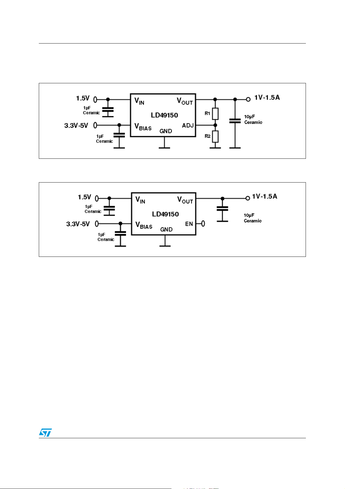
1 Typical application circuits
Figure 1. Adjustable version
Figure 2. Fixed version with Enable
Doc ID 13446 Rev 3 3/22
Alternative application circuits LD49150XX08, LD49150XX10, LD49150XX12
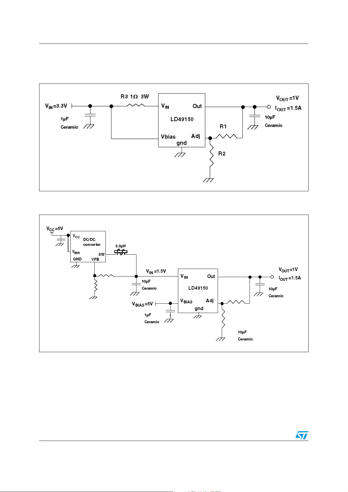
2 Alternative application circuits
Figure 3. Single supply voltage solution
Figure 4. LD49150xx plus DC-DC pre-regulator to reduce power dissipation
4/22 Doc ID 13446 Rev 3
LD49150XX08, LD49150XX10, LD49150XX12 Pin configuration
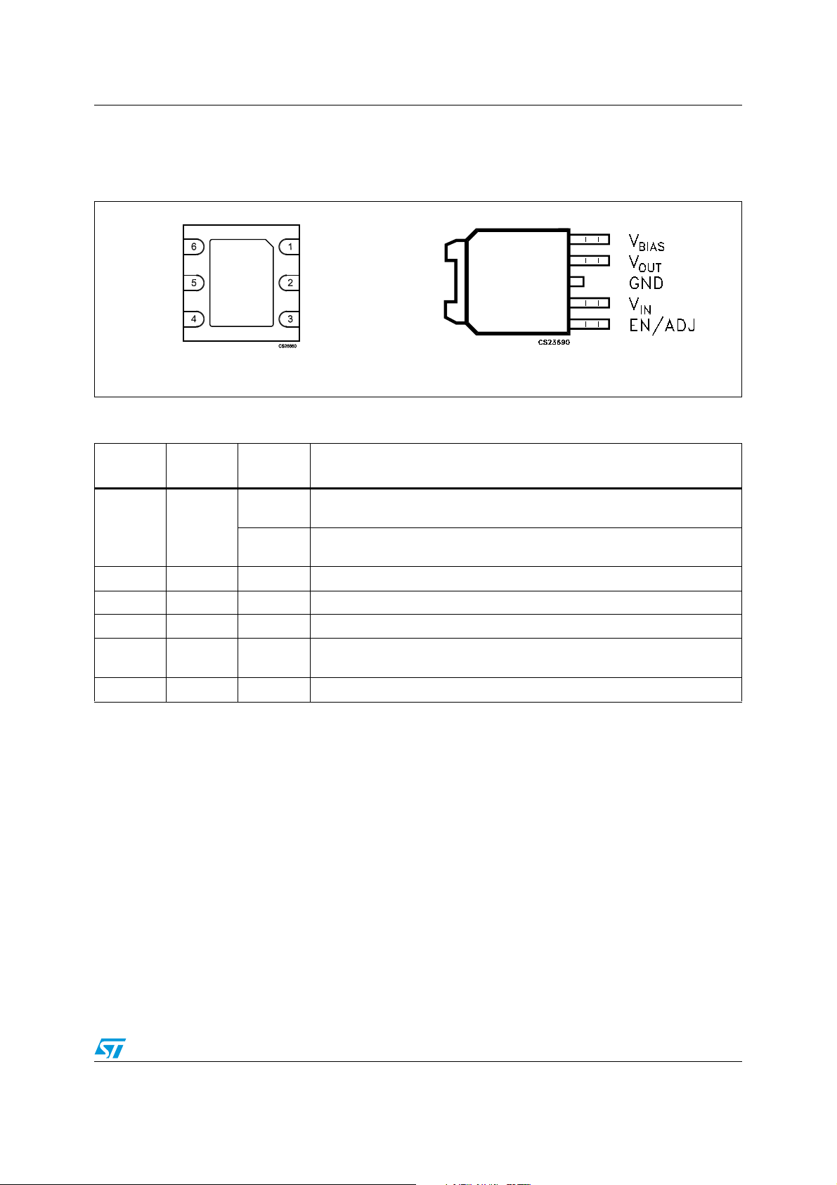
3 Pin configuration
Figure 5. Pin connections (top view for PPAK, bottom view for DFN)
DFN6 (3 x 3 mm)
Table 2. Pin description
Pin n° for
PPAK
12
23V
3 1 GND Ground (TAB is connected to ground).
44V
56V
Pin n° for
DFN
Symbol Note
EN
ADJ
OUT
BIAS
For fixed versions: Enable (Input) - Logic High = Enable, Logic Low =
Shutdown.
For adjustable versions: Adjustable regulator feedback input. Connect to
resistor voltage divider.
Input voltage which supplies current to the output power device.
IN
Regulator output.
Input bias voltage for powering all circuitry on the regulator with the
exception of the output power device.
5 N.C. Not connect.
PPAK
Doc ID 13446 Rev 3 5/22
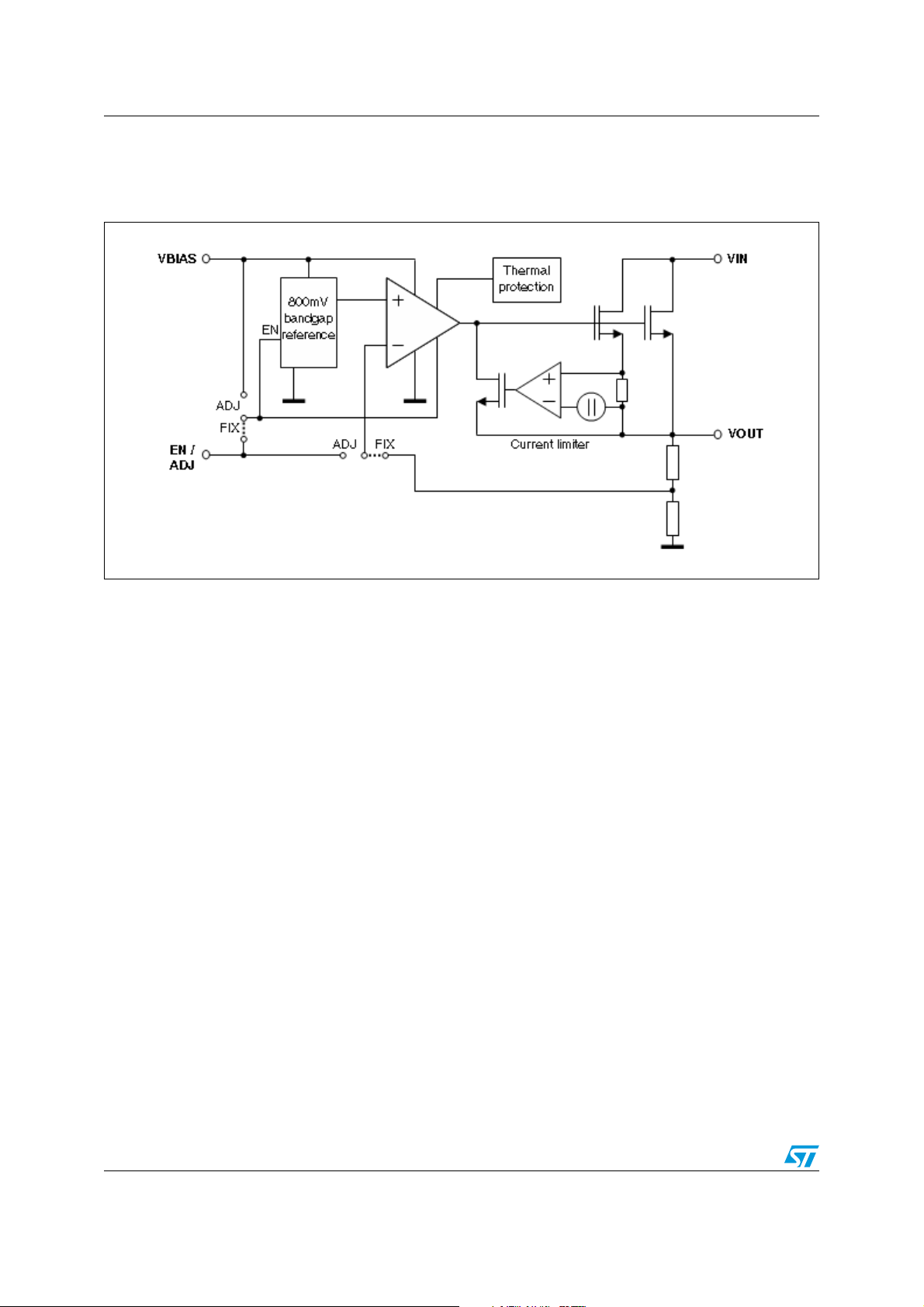
Diagram LD49150XX08, LD49150XX10, LD49150XX12
4 Diagram
Figure 6. Block diagram
6/22 Doc ID 13446 Rev 3
LD49150XX08, LD49150XX10, LD49150XX12 Maximum ratings
5 Maximum ratings
Table 3. Absolute maximum ratings
(1)
Symbol Parameter Value Unit
V
IN
V
OUT
V
BIAS
V
EN
P
D
T
STG
1. All the values are referred to ground.
Supply voltage -0.3 to 7 V
Output voltage
-0.3 to V
-0.3 to V
IN
BIAS
+ 0.3
+ 0.3
V
BIAS supply voltage -0.3 to 7 V
Enable input voltage -0.3 to 7 V
Power dissipation Internally limited
Storage temperature range -50 to 150 °C
Note: Absolute maximum ratings are those values beyond which damage to the device may occur.
Functional operation under these conditions is not implied.
Table 4. Operating ratings
Symbol Parameter Value Unit
V
V
V
OUT
BIAS
V
EN
T
IN
J
Supply voltage 1.4 to 5.5 V
Output voltage 0.8 to 4.5 V
BIAS supply voltage 3 to 6 V
Enable input voltage 0 to V
BIAS
V
Junction temperature range -25 to 125 °C
Doc ID 13446 Rev 3 7/22

Electrical characteristics LD49150XX08, LD49150XX10, LD49150XX12
6 Electrical characteristics
TJ = - 25 °C to 125 °C, V
1 µF; C
= 10 µF; C
O
BIAS
= 1 µF; unless otherwise specified.
BIAS
Typical values are referred to T
Table 5. Electrical characteristics
= VO + 2.1 V
= 25 °C.
J
(1)
; VI = VO+1 V; VEN = V
BIAS
(2)
, IO = 10 mA; CI =
Symbol Parameter Test conditions Min. Typ. Max. Unit
T
= 25 °C, fixed voltage options -1.5 1.5
V
O
V
LINE
V
LOAD
V
DROP
V
DROP
I
GND
I
GND_SHD
Output voltage accuracy
Line regulation VI = VO + 1 V to 5.5 V -0.1 0.1 %/V
Load regulation IL = 0 mA to 3 A, V
Dropout voltage (VI - VO)I
Dropout voltage (V
- VO)I
BIAS
Ground pin current
Ground pin current in shutdown VEN ≤ 0.4 V
J
Over temperature range -3 3
≥ 3 V 1 %
BIAS
= 1.5 A 200 mV
L
= 1.5 A
L
I
= 0 mA 4 6
L
= 1.5 A 4 6
I
L
(1)
(2)
1.5 2.1 V
5µA
IL = 0 mA 3 5
I
VBIAS
I
Enable input
Current through V
Current limit VO = 0 V 2.5 A
L
(2)
BIAS
= 1.5 A 3 5
I
L
%
mA
mA
V
I
EN
Enable input threshold (fixed
EN
voltage only)
Enable pin input current 0.1 1 µA
Reference
V
REF
Reference voltage
SVR Supply voltage rejection
1. For VO ≤ 1 V, V
2. Fixed output voltage version only.
dropout specification does not apply due to a minimum 3 V V
BIAS
Regulator Enable 1.4
Regulator Shutdown 0.4
T
= 25 °C 0.788 0.8 0.812
J
Over temperature range 0.776 0.8 0.824
= 2.5 V ± 0.5 V, VO = 1 V,
V
I
F = 120 Hz, V
BIAS
= 3.3 V
BIAS
input.
68 dB
V
V
8/22 Doc ID 13446 Rev 3

LD49150XX08, LD49150XX10, LD49150XX12 Typical characteristics
7 Typical characteristics
Figure 7. Reference voltage vs. temperature Figure 8. Output voltage vs. temperature
Figure 9. Load regulation vs. temperature Figure 10. Line regulation vs. temperature
Figure 11. Output voltage vs. input voltage Figure 12. Dropout voltage (VIN-V
Doc ID 13446 Rev 3 9/22
temperature
OUT
) vs.

Typical characteristics LD49150XX08, LD49150XX10, LD49150XX12
Figure 13. Dropout voltage (VIN-V
Figure 15. Noise vs. frequency Figure 16. Quiescent current vs. temperature
temperature
OUT
) vs.
Figure 14. V
pin current vs. temperature
BIAS
Figure 17. Supply voltage rejection vs. output
current
Figure 18. Stability region vs. C
10/22 Doc ID 13446 Rev 3
ESR
OUT
& High

LD49150XX08, LD49150XX10, LD49150XX12 Typical characteristics
Figure 19. Stability region vs. C
& low ESR Figure 20. V
OUT
Figure 21. VIN start up transient response
(V
start up before VIN)
BIAS
VIN=V
BIAS=VINH
Figure 22. V
& VIN start up transient
BIAS
response (V
and V
IN
BIAS
the same time)
=3.1V, V
start up transient response
IN
(V
BIAS
OUT
=1V, C
OUT
=1µF
start up before VIN)
start up at
VIN=2.5V, V
BIAS=VINH
=3.1V, V
OUT
=1V, C
OUT
=1µF
VIN=2.5V, V
BIAS=VINH
=3.1V, V
OUT
=1V, C
OUT
=1µF
Doc ID 13446 Rev 3 11/22

Typical characteristics LD49150XX08, LD49150XX10, LD49150XX12
Figure 23. VIN start up transient response
(V
start up before V
BIAS
V
INH=VIN
)
IN
and
VIN=V
=2.5V, V
INH
BIAS
=3.1V, V
OUT
=1V, C
OUT
=1µF
12/22 Doc ID 13446 Rev 3

LD49150XX08, LD49150XX10, LD49150XX12 Application hints
8 Application hints
The LD49150xx is an ultra-high performance, low dropout linear regulator, designed for high
current application that requires fast transient response. The LD49150xx operates from two
input voltages, to reduce dropout voltage. The LD49150xx is designed so that a minimum of
external component are necessary.
8.1 Input supply voltage (VIN)
VIN provides the power input current to the LD49150xx. The minimum input voltage can be
as low as 1.4 V, allowing conversion from very low voltage supplies to achieve low output
voltage levels with very low power dissipation.
8.2 Bias supply voltage (V
The LD49150xx control circuitry is supplied the V
current (3 mA typ.) even at the maximum output current level (1.5 A). A bypass capacitor on
the bias pin is recommended to improve the performance of the LD49150xx during line and
load transient. The small ceramic capacitor from V
noise that could be injected into the control circuitry from the bias rail. In typical applications
a 1 µF ceramic chip capacitor may be used. The V
the output voltage, with a minimum V
8.3 External capacitors
To assure regulator stability, input and output capacitors are required as shown in the 1:
Typical application circuits.
8.4 Output capacitor
The LD49150xx requires a minimum output capacitance to maintain stability. A ceramic chip
capacitor of at least 1 µF is required. However, specific capacitor selection could be needed
to ensure the transient response. A 1 µF ceramic chip capacitor satisfies most applications
but 10 µF is recommended to ensure better transient performances. In applications where
the V
recommended to use an output capacitors of, at least, 10 µF in order to avoid over-voltage
stress on the Input/output power pins during short circuit conditions due to parasitic
inductive effect. The output capacitor must be located as close as possible to the output pin
of the LD49150xx. The ESR (equivalent series resistance) of the output capacitor must be
within the "stable" region as shown in the typical characteristics figures. Both ceramic and
tantalum capacitors are suitable.
level is close to the maximum operating voltage (V
IN
BIAS
BIAS
)
pin which requires a very low bias
BIAS
to ground reduces high frequency
BIAS
input voltage must be 2.1 V above
input voltage of 3 V.
BIAS
> 4 V), it is strongly
IN
8.5 Minimum load current
The LD49150xx does not require a minimum load to maintain output voltage regulation.
Doc ID 13446 Rev 3 13/22

Application hints LD49150XX08, LD49150XX10, LD49150XX12
8.6 Power sequencing recommendations
In order to ensure the correct biasing and settling of the regulator internal circuitry during the
startup phase, as well as to avoid overvoltage spikes at the output, it is recommended to
provide for the correct power sequencing.
As a general rule the V
and V
IN
signals timings at startup should be chosen properly, so
INH
that they are applied to the device after the V
operative value (see paragraph 8.2: Bias supply voltage (VBIAS)). This can be achieved, for
instance, by avoiding too slow V
rising edges (Tr >10 ms).
BIAS
Provided that the above condition is satisfied, when fast V
present, a smooth startup, with limited overvoltage on the output, can be obtained by
applying V
voltage at the same time as the V
IN
and Figure 22 on page 11).
In the fixed voltage versions it is possible to reduce overvoltage spikes during very fast
startup (T
<< 100 µs) by pulling the V
r
pin up to VIN voltage (see Figure 23 on page 12).
INH
8.7 Power dissipation/heatsinking
A heatsink may be required depending on the maximum power dissipation and maximum
ambient temperature of the application. Under all possible conditions, the junction
temperature must be within the range specified under operating conditions. The total power
dissipation of the device is given by:
P
= VIN x IIN + V
D
Where:
● V
● V
● V
● I
, input supply voltage
IN
, bias supply voltage
BIAS
, output voltage
OUT
, load current
OUT
From this data, we can calculate the thermal resistance (
using the following formula:
BIAS
x I
BIAS
- V
OUT
x I
OUT
voltage is already settled at its minimum
BIAS
transient input (Tr < 100 µs) is
IN
voltage (refer to Figure 20, Figure 21
BIAS
θ
) required for the heat sink
SA
θ
= (TJ - TA/PD) - (θJC + θCS)
SA
The maximum allowed temperature rise (T
temperature (T
(T
):
Jmax
T
= T
Rmax
Jmax
) of the application, and the maximum allowable junction temperature
Amax
- T
Amax
Rmax
The maximum allowable value for junction to ambient thermal resistance, θJA, can be
calculated using the formula:
θ
JAmax
= T
Rmax
/ P
D
This part is available for the PPAK package.
The thermal resistance depends on the amount of copper area or heat sink, and on air flow.
If the maximum allowable value of
θ
calculated above is ≥ 100 °C/W for the PPAK
JA
package, no heatsink is needed since the package can dissipate enough heat to satisfy
these requirements. If the value for allowable
θ
required as described below.
14/22 Doc ID 13446 Rev 3
) depends on the maximum ambient
falls below these limits, a heat sink is
JA

LD49150XX08, LD49150XX10, LD49150XX12 Application hints
8.8 Heatsinking PPAK package
The PPAK package uses the copper plane on the PCB as a heatsink. The tab of these
packages is soldered to the copper plane for heat sinking. It is also possible to use the PCB
ground plane a heatsink. This area can be the inner GND layer of a multi-layer PCB, or, in a
dual layer PCB, it can be an unbroken GND area on the opposite side where the IC is
situated with a dissipating area thermally connected through vias holes, filled by solder.
Figure 26 shows a curve for
θ
of the PPAK package for different copper area sizes, using
JA
a typical PCB with 1/16 in thick G10/FR4.
θ
Figure 24.
vs. copper area for PPAK package
JA
8.9 Adjustable regulator design
The LD49150xx adjustable version allows fixing output voltage anywhere between 0.8 V and
4.5 V using two resistors as shown in the typical application circuit. For example, to fix the
R
resistor value between V
1
(R
) is calculated by:
2
R
= R1 [0.8/(V
2
Where V
It is suggested to use R1 values lower than 10 kΩ to obtain better load transient
performances. Even, higher values up to 100 kΩ are suitable.
8.10 Enable
The fixed output voltage versions of LD49150xx feature an active high Enable input (EN)
that allows on-off control of the regulator. The EN input threshold is guaranteed between 0.4
V and 1.4 V, for simple logic interfacing. The regulator is set in shut down mode when V
0.4 V and it is in operating mode (V
must be tied directly to the V
not be left at high impedance.
and the ADJ pin, the resistor value between ADJ and GND
OUT
- 0.8)]
OUT
is the desired output voltage.
OUT
to keep the regulator continuously activated. The En pin must
IN
Doc ID 13446 Rev 3 15/22
activated) when V
OUT
> 1.4 V. If not in use, the EN pin
EN
EN
<

Package mechanical data LD49150XX08, LD49150XX10, LD49150XX12
9 Package mechanical data
In order to meet environmental requirements, ST offers these devices in different grades of
ECOPACK
specifications, grade definitions and product status are available at: www.st.com.
ECOPACK
®
packages, depending on their level of environmental compliance. ECOPACK®
®
is an ST trademark.
16/22 Doc ID 13446 Rev 3

LD49150XX08, LD49150XX10, LD49150XX12 Package mechanical data
PPAK mechanical data
Dim.
Min. Typ. Max. Min. Typ. Max.
A 2.2 2.4 0.086 0.094
A1 0.9 1.1 0.035 0.043
A2 0.03 0.23 0.001 0.009
B 0.4 0.6 0.015 0.023
B2 5.2 5.4 0.204 0.212
C 0.45 0.6 0.017 0.023
C2 0.48 0.6 0.019 0.023
D 6 6.2 0.236 0.244
D1 5.1 0.201
E 6.4 6.6 0.252 0.260
E1 4.7 0.185
e 1.27 0.050
G4.9 5.25 0.193 0.206
G1 2.38 2.7 0.093 0.106
H 9.35 10.1 0.368 0.397
L2 0.8 1 0.031
L4 0.6 1 0.023 0.039
L5 1
L6 2.8 0.110
mm. inch.
0.039
0.039
0078180-E
Doc ID 13446 Rev 3 17/22

Package mechanical data LD49150XX08, LD49150XX10, LD49150XX12
DFN6 (3x3 mm) mechanical data
mm. inch.
Dim.
Min. Typ. Max. Min. Typ. Max.
A0.800.90 1.00 0.031 0.035 0.039
A1 0 0.02 0.05 0 0.001 0.002
A3 0.20 0.008
b 0.23 0.300.38 0.009 0.012 0.015
D2.90 3.00 3.10 0.114 0.118 0.122
D2 2.23 2.38 2.48 0.088 0.094 0.098
E2.90 3.00 3.10 0.114 0.118 0.122
E2 1.50 1.65 1.75 0.059 0.065 0.069
e0.950.037
L0.30 0.40 0.50 0.012 0.016 0.020
18/22 Doc ID 13446 Rev 3
7946637A

LD49150XX08, LD49150XX10, LD49150XX12 Package mechanical data
Tape & reel DPAK-PPAK mechanical data
Dim.
Min. Typ. Max. Min. Typ. Max.
A 330 12.992
C12.8 13.0 13.2 0.504 0.512 0.519
D 20.2 0.795
N60 2.362
T22.40.882
Ao 6.806.90 7.00 0.268 0.272 0.2.76
Bo 10.40 10.50 10.60 0.409 0.413 0.417
Ko 2.55 2.65 2.75 0.100 0.104 0.105
Po 3.9 4.0 4.1 0.153 0.157 0.161
P7.98.0 8.1 0.311 0.315 0.319
mm. inch.
Doc ID 13446 Rev 3 19/22

Package mechanical data LD49150XX08, LD49150XX10, LD49150XX12
Tape & reel QFNxx/DFNxx (3x3) mechanical data
mm. inch.
Dim.
Min. Typ. Max. Min. Typ. Max.
A180 7.087
C 12.8 13.2 0.504 0.519
D 20.2 0.795
N60 2.362
T 14.4 0.567
Ao 3.3 0.130
Bo 3.3 0.130
Ko 1.1 0.043
Po 4 0.157
P 8 0.315
20/22 Doc ID 13446 Rev 3

LD49150XX08, LD49150XX10, LD49150XX12 Revision history
10 Revision history
Table 6. Document revision history
Date Revision Changes
18-Apr-2007 1 Initial release.
12-Jan-2009 2 Added new package DFN6 (3x3 mm) and mechanical data.
29-Jun-2010 3 Modified Section 8.6: Power sequencing recommendations on page 14.
Doc ID 13446 Rev 3 21/22

LD49150XX08, LD49150XX10, LD49150XX12
Please Read Carefully:
Information in this document is provided solely in connection with ST products. STMicroelectronics NV and its subsidiaries (“ST”) reserve the
right to make changes, corrections, modifications or improvements, to this document, and the products and services described herein at any
time, without notice.
All ST products are sold pursuant to ST’s terms and conditions of sale.
Purchasers are solely responsible for the choice, selection and use of the ST products and services described herein, and ST assumes no
liability whatsoever relating to the choice, selection or use of the ST products and services described herein.
No license, express or implied, by estoppel or otherwise, to any intellectual property rights is granted under this document. If any part of this
document refers to any third party products or services it shall not be deemed a license grant by ST for the use of such third party products
or services, or any intellectual property contained therein or considered as a warranty covering the use in any manner whatsoever of such
third party products or services or any intellectual property contained therein.
UNLESS OTHERWISE SET FORTH IN ST’S TERMS AND CONDITIONS OF SALE ST DISCLAIMS ANY EXPRESS OR IMPLIED
WARRANTY WITH RESPECT TO THE USE AND/OR SALE OF ST PRODUCTS INCLUDING WITHOUT LIMITATION IMPLIED
WARRANTIES OF MERCHANTABILITY, FITNESS FOR A PARTICULAR PURPOSE (AND THEIR EQUIVALENTS UNDER THE LAWS
OF ANY JURISDICTION), OR INFRINGEMENT OF ANY PATENT, COPYRIGHT OR OTHER INTELLECTUAL PROPERTY RIGHT.
UNLESS EXPRESSLY APPROVED IN WRITING BY AN AUTHORIZED ST REPRESENTATIVE, ST PRODUCTS ARE NOT
RECOMMENDED, AUTHORIZED OR WARRANTED FOR USE IN MILITARY, AIR CRAFT, SPACE, LIFE SAVING, OR LIFE SUSTAINING
APPLICATIONS, NOR IN PRODUCTS OR SYSTEMS WHERE FAILURE OR MALFUNCTION MAY RESULT IN PERSONAL INJURY,
DEATH, OR SEVERE PROPERTY OR ENVIRONMENTAL DAMAGE. ST PRODUCTS WHICH ARE NOT SPECIFIED AS "AUTOMOTIVE
GRADE" MAY ONLY BE USED IN AUTOMOTIVE APPLICATIONS AT USER’S OWN RISK.
Resale of ST products with provisions different from the statements and/or technical features set forth in this document shall immediately void
any warranty granted by ST for the ST product or service described herein and shall not create or extend in any manner whatsoever, any
liability of ST.
ST and the ST logo are trademarks or registered trademarks of ST in various countries.
Information in this document supersedes and replaces all information previously supplied.
The ST logo is a registered trademark of STMicroelectronics. All other names are the property of their respective owners.
© 2010 STMicroelectronics - All rights reserved
STMicroelectronics group of companies
Australia - Belgium - Brazil - Canada - China - Czech Republic - Finland - France - Germany - Hong Kong - India - Israel - Italy - Japan -
Malaysia - Malta - Morocco - Philippines - Singapore - Spain - Sweden - Switzerland - United Kingdom - United States of America
www.st.com
22/22 Doc ID 13446 Rev 3
 Loading...