

ST LD39115J08R, LD39115J10R User Manual
Features
■ Input voltage from 1.5 to 5.5 V
■ Ultra low dropout voltage (80 mV typ. at 100
mA load)
■ Very low quiescent current (20 µA typ. at no
load, 35 µA typ. at 150 mA load, 1 µA max in off
mode)
■ Very low noise (33 µV
kHz at V
■ Output voltage tolerance: ± 2.0 % @ 25 °C
■ 150 mA guaranteed output current
■ Wide range of output voltages available on
OUT
= 1.8 V)
from 1 kHz to 100
RMS
request: 0.8 V to 4.5 V with 100 mV step
■ Logic-controlled electronic shutdown
■ Compatible with ceramic capacitor C
■ Internal current and thermal limit
■ Flip-chip 4 bumps 0.8 x 0.8 mm. pitch
■ Temperature range: -40 °C to 125 °C
OUT
= 1 µF
Applications
■ Mobile phones
■ Personal digital assistants (PDAs)
■ Cordless phones and similar battery-powered
systems
Table 1. Device summary
LD39115Jxx
150 mA low quiescent current
low noise voltage regulator
Flip-chip 4
Description
The LD39115Jxx provides 150 mA maximum
current from an input voltage ranging from 1.5 V
to 5.5 V with a typical dropout voltage of 80 mV. It
is stabilized with a ceramic capacitor. The ultra
low drop voltage, low quiescent current and low
noise features make it suitable for low power
battery-powered applications. Power supply
rejection is 65 dB at low frequencies and starts to
roll off at 10 kHz. An enable logic control function
puts the LD39115Jxx in shutdown mode allowing
a total current consumption lower than 1 µA. The
device also includes a short-circuit constant
current limiting and thermal protection.
Part numbers Order codes Output voltages
LD39115JXX12 LD39115J12R 1.2 V
LD39115JXX15 LD39115J15R 1.5 V
LD39115JXX18 LD39115J18R 1.8 V
LD39115JXX25 LD39115J25R 2.5 V
LD39115JXX28 LD39115J28R 2.8 V
LD39115JXX30 LD39115J30R 3.0 V
LD39115JXX33 LD39115J33R 3.3 V
December 2011 Doc ID 15527 Rev 5 1/23
www.st.com
23

Contents LD39115Jxx
Contents
1 Diagram . . . . . . . . . . . . . . . . . . . . . . . . . . . . . . . . . . . . . . . . . . . . . . . . . . . 3
2 Pin configuration . . . . . . . . . . . . . . . . . . . . . . . . . . . . . . . . . . . . . . . . . . . 4
3 Typical application . . . . . . . . . . . . . . . . . . . . . . . . . . . . . . . . . . . . . . . . . . 5
4 Maximum ratings . . . . . . . . . . . . . . . . . . . . . . . . . . . . . . . . . . . . . . . . . . . . 6
5 Electrical characteristics . . . . . . . . . . . . . . . . . . . . . . . . . . . . . . . . . . . . . 7
6 Typical performance characteristics . . . . . . . . . . . . . . . . . . . . . . . . . . . 11
7 Package mechanical data . . . . . . . . . . . . . . . . . . . . . . . . . . . . . . . . . . . . 17
8 Different output voltage versions of the LD39115Jxx
available on request . . . . . . . . . . . . . . . . . . . . . . . . . . . . . . . . . . . . . . . . 21
9 Revision history . . . . . . . . . . . . . . . . . . . . . . . . . . . . . . . . . . . . . . . . . . . 22
2/23 Doc ID 15527 Rev 5
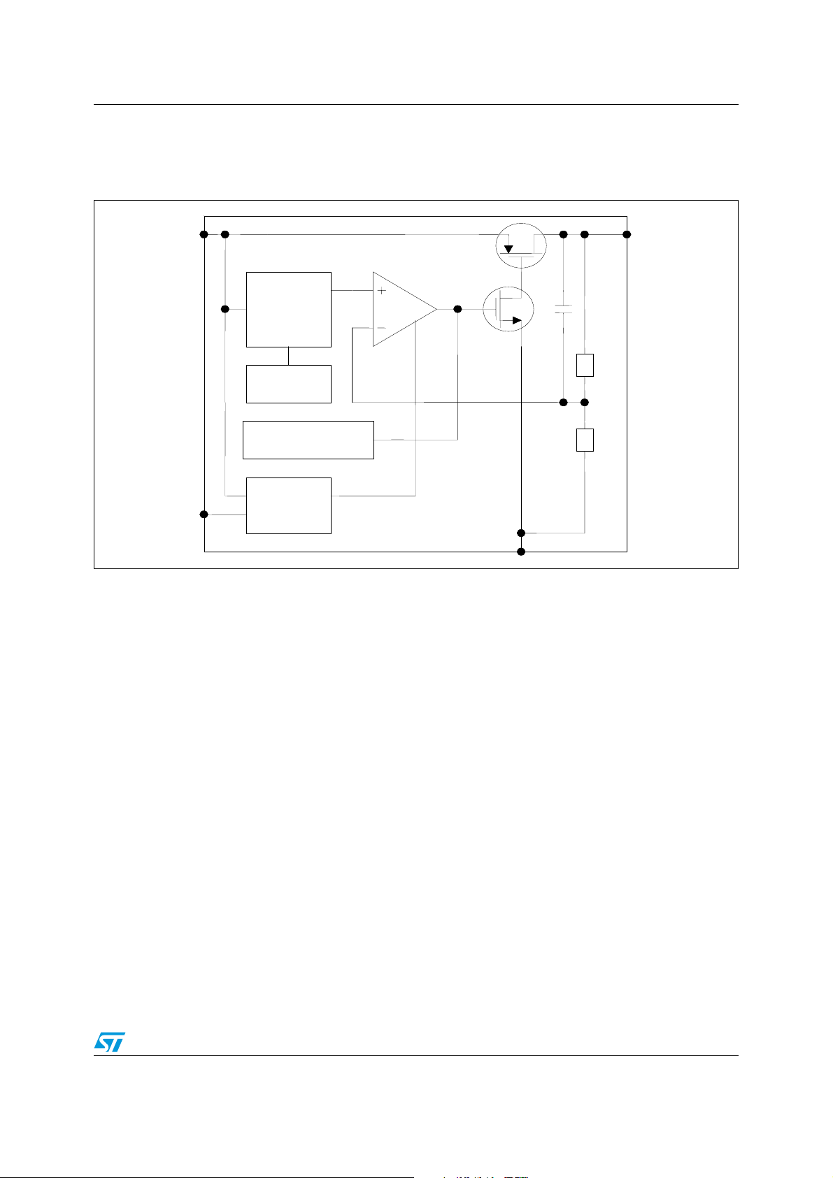
LD39115Jxx Diagram
1 Diagram
Figure 1. Block diagram
OUT
IN
IN
BandGap
BandGap
1.22 V
1.22 V
Trimming
Trimming
Thermal
Thermal
Protection
Protection
OUT
R1
R1
R2
R2
EN
EN
Enable
Enable
GND
GND
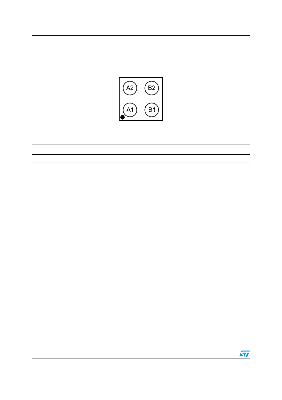
Pin configuration LD39115Jxx
2 Pin configuration
Figure 2. Pin connection (top view)
Table 2. Pin description
Pin n° Symbol Function
A2 EN Enable pin logic input: Low = shutdown, High = active
A1 GND Common ground
B2 IN Input voltage of the LDO
B1 OUT Output voltage
4/23 Doc ID 15527 Rev 5
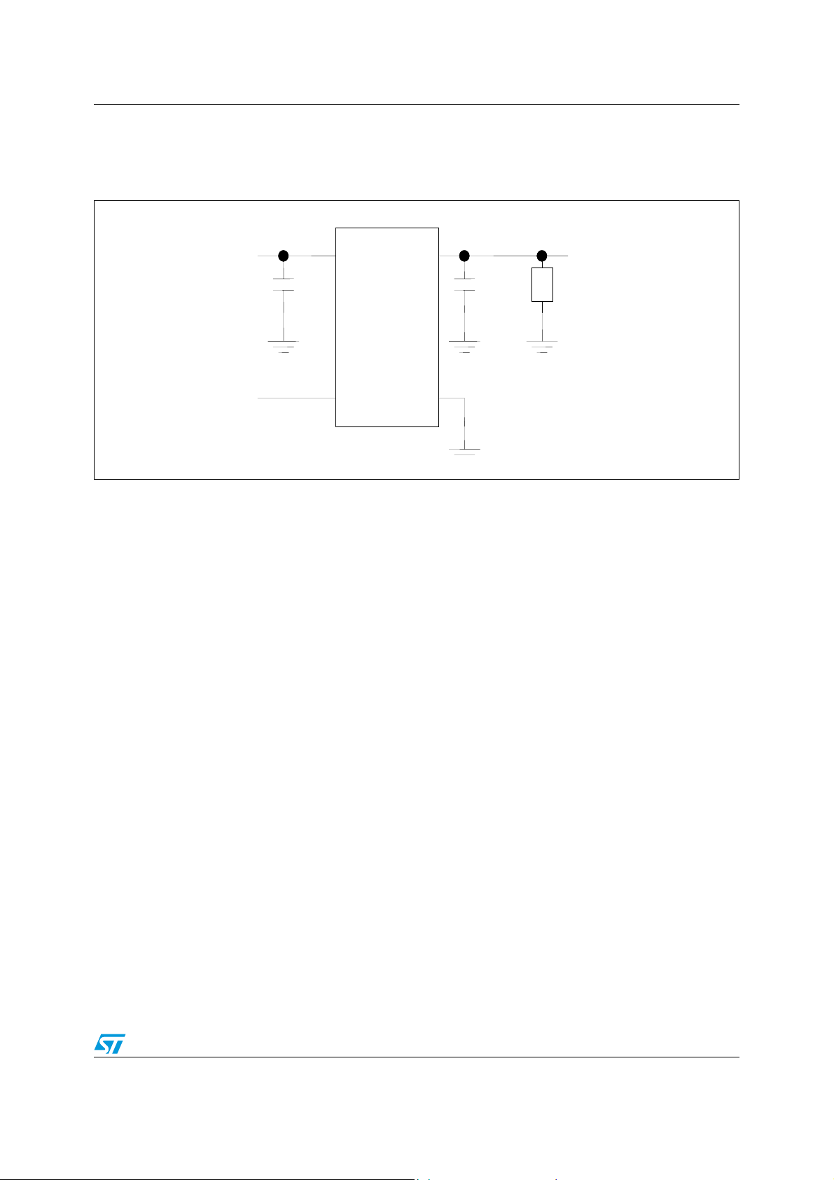
LD39115Jxx Typical application
3 Typical application
Figure 3. Typical application circuit
V
V
V
IN
IN
IN
IN
OUT
OUT
V
OUT
OUT
1 µF
1 µF
V
V
EN
EN
EN
EN
GND
GND
1 µF
1 µF
Load
Load
Doc ID 15527 Rev 5 5/23
Maximum ratings LD39115Jxx
4 Maximum ratings
Table 3. Absolute maximum ratings
Symbol Parameter Value Unit
V
V
I
T
T
V
IN
OUT
EN
OUT
P
D
STG
OP
DC input voltage - 0.3 to 6 V
DC output voltage - 0.3 to VI + 0.3 V
Enable input voltage - 0.3 to VI + 0.3 V
Output current Internally limited mA
Power dissipation Internally limited mW
Storage temperature range - 65 to 150 °C
Operating junction temperature range - 40 to 125 °C
Note: Absolute maximum ratings are those values beyond which damage to the device may occur.
Functional operation under these conditions is not implied. All values are referred to GND.
Table 4. Thermal data
Symbol Parameter Value Unit
R
thJA
Thermal resistance junction-ambient 180 °C/W
6/23 Doc ID 15527 Rev 5
LD39115Jxx Electrical characteristics
5 Electrical characteristics
TJ = 25 °C, V
IN
= V
OUT(NOM)
+ 1 V, CIN = C
otherwise specified.
Table 5. Electrical characteristics for LD39115Jxx
Symbol Parameter Test conditions Min. Typ. Max. Unit
V
IN
V
UVLO
V
OUT
ΔV
OUT
ΔV
OUT
ΔV
OUT
ΔV
OUT
V
DROP
e
N
SVR
I
Q
I
SC
V
EN
I
EN
T
ON
Operating input voltage 1.5 5.5 V
Turn-on threshold 1.45 1.48 V
Turn-off threshold 1.30 1.35 mV
>1.5V, I
V
OUT
>1.5V, I
V
V
OUT
accuracy
OUT
-40°C<T
V
OUT
V
OUT
<125°C
J
≤ 1.5V, I
≤ 1.5V, I
-40°C<TJ<125°C
Static line regulation V
Transient line regulation
(2)
Static load regulation I
Transient load
regulation
Dropout voltage
(2)
(3)
+1V ≤ VIN ≤ 5.5V, I
OUT
ΔVIN=+500mV, I
TR=TF=5µs
=1mA to 150mA 0.002 %/mA
OUT
I
=1mA to 150mA, tR=tF=5µs 40 mVpp
OUT
I
=100mA, V
OUT
-40°C<T
<125°C
J
Output noise voltage 10Hz to 100kHz, I
V
IN=VOUTNOM
Supply voltage rejection
= 1.5V
V
OUT
Quiescent current
V
I
V
V
I
I
I
I
I
V
=0.1V Freq.=1kHz
RIPPLE
= 10mA
OUT
IN=VOUTNOM
=0.1V Freq.=10kHz
RIPPLE
=10mA
OUT
=0mA 20
OUT
=0mA, -40°C<TJ<125°C 50
OUT
=0 to 150mA 35
OUT
=0 to 150mA, -40°C<TJ<125°C 70
OUT
input current in OFF MODE:
IN
VEN=GND
Short circuit current RL=0 200 mA
Enable input logic low VIN=1.5V to5.5V, -40°C<TJ<125°C 0.4
Enable input logic high V
Enable pin input current V
Turn on time
(4)
=1.5V to 5.5V, -40°C<TJ<125°C 0.9
IN
SHDN=VIN
= 1 µF, I
OUT
(1)
=1mA, TJ=25°C -2.0 2.0 %
OUT
=1mA,
OUT
=1mA ±10 mV
OUT
=1mA,
OUT
=1mA 0.01 %/V
OUT
=1mA,
OUT
>1.5V
OUT
=10mA 30 µV
OUT
+1V+/-V
RIPPLE
= 1 mA, VEN = VIN, unless
OUT
-3.0 3.0 %
±30 mV
10 mVpp
80 110 mV
74
+0.5V+/-V
RIPPLE
67
0.001 1
0.1 100 nA
30 µs
RMS
dB
µA
V
/V
Doc ID 15527 Rev 5 7/23
 Loading...